

Motorola MCD221FU Datasheet
SEMICONDUCTOR TECHNICAL DATA
Technical Summary
This technical summary provides a brief description of the MCD221
CD–Interface and Audio Processor. A complete data sheet for the MCD221 is
available and can be ordered from your local Motorola sales office. The order
number is MCD221/D.
The MCD221 has two main functions. The first is to form an interface
between a CD drive unit and a CD–i or Photo–CD player. The connection to the
drive is designed for both applications and can be either a Digital Out (EBU
standard) interface, or an I2S plus subcode interface. The host interface can be
either a 68000 interface for CD–i players, or a serial (SPI) interface for
Photo–CD.
The second function of the MCD221 is to decode ADPCM (CD–i base case)
audio, to perform audio mixing functions as specified in the Green Book, and to
be able to add external audio to the base case audio. The MCD221 can also be
used for handling the ADPCM decoding for Photo–CD.
The main features of the MCD221 are as follows:
• Accepts Audio Inputs in I2S Format (MPEG1) for Mixing with CIAP Internal
Audio
• Output Can Be Either I2S or SONY Format
• Data Input Rate Can Be Up to 2 Times Normal Speed
• Can Connect to a Host via Either a 68K or Serial Interface
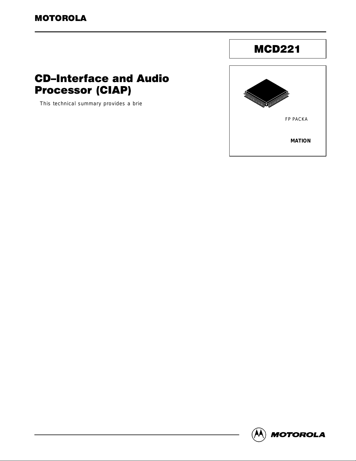
• 80–Pin Quad Flat Pack (QFP)
Order this document
by MCD221TS/D
FU SUFFIX
QFP PACKAGE
CASE 841B–01
ORDERING INFORMATION
MCD221FU QFP
NOTE: Supply of this Video–CD IC does not convey an implied license under any patent right to use this IC in any Video–CD application.
CD–i is a registered trademark of Philips Consumer Electronics.
Motorola, Inc. 1995
MOTOROLA
REV 0
2/95
MCD221
2–1
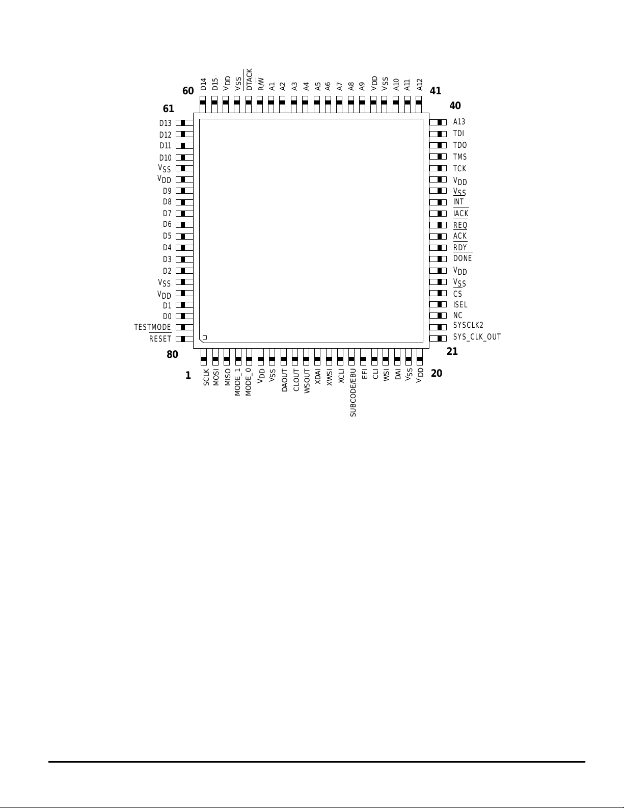
61
D13
D12
D11
D10
V
SS
V
DD
D9
D8
D7
D6
D5
D4
D3
D2
V
SS
V
DD
D1
D0
TESTMODE
RESET
80
D14
D15
VDDVSSDTACK
PIN ASSIGNMENT
R/WA1A2A3A4A5A6A7A8A9VDDVSSA10
A11
A12
4160
40
A13
TDI
TDO
TMS
TCK
V
DD
V
SS
INT
IACK
REQ
ACK
RDY
DONE
V
DD
V
SS
CS
ISEL
NC
SYSCLK2
SYS_CLK_OUT
21
20
SS
1
MOSI
SCLK
MISO
MODE_1
SS
DD
V
V
MODE_0
CLOUT
DAOUT
XDAI
WSOUT
XCLI
XWSI
SUBCODE/EBU
EFI
CLI
WSI
DAI
DD
V
V
MCD221
2–2
MOTOROLA
PIN DESCRIPTIONS
Ï
Ï
Ï
Ï
Ï
Ï
Î
Î
Î
Ï
Ï
Ï
SIGNAL DESCRIPTIONS
Host Interface
Mnemonic Type Name and Function
A[13 … 1] O System Address Bus. The address must be stable before CS
D[15 … 0] B System Data Bus. The data lines must be stable when CS
CS
R/W
DTACK
INT
IACK
REQ
ACK
RDY
DONE
Active HIGH.
a write and before DTACK
is asserted during a read. Tri–state.
I Chip Select. Used to access the CIAP internal registers and buffers.
Active LOW.
I Read/Write. Indicates the direction of the data transfer. When LOW, the
transfer is to the CIAP.
B Data Transfer Acknowledge. Active LOW. During normal host access,
DTACK
is an output indicating that data has been put on (read cycles) or
read from (write cycles) the data bus. (Active pullup.) During DMA,
DTACK
is an input indicating that the memory has put data on the data
bus.
O Interrupt. Released when the interrupt status register is read. Active
LOW.
I Interrupt Acknowledge. Active LOW.
O DMA Request. Active LOW.
I Acknowledge. DMA handshake signal indicating that the bus is available
for data transfer. Active LOW .
O Ready. DMA handshake signal indicating that the CIAP has completed
the data transfer. Tri–state. Active LOW. When released by the CIAP, the
output is forced high for a few nanoseconds before it is made tri–state.
I Done. Indicates the last transfer of a DMA burst. Active LOW.
is asserted.
is active during
Serial Interface
Mnemonic Type Name and Function
SCLK
MOSI
MISO
MODE_0,
MODE_1
ÏÏÏÏ
ÏÏÏÏ
I
Serial Clock.
I
Serial Data. Master out, slave in.
O
Serial Data. Master in, slave out.
I
Serial Interface MODE bits.
00 = Write selected register
Ï
Ï
ПППППППППППППППП
01 = Read selected register
10 = Write address
ПППППППППППППППП
11 = No action
Data Input
Mnemonic Type Name and Function
CLI
WSI
DAI
EFI
SUBCODE/EBU
I
Serial Bit Clock Input.
I
Word Clock Input.
I
Serial Data Input.
I
Error Flag Input.
I
Subcode (P … W) serial data input or EBU input for both main channel
and subchannel.
External Audio Interface
Mnemonic Type Name and Function
XCLI
ÎÎÎÎ
XWSI
ÏÏÏÏ
XDAI
I
External Audio Serial Bit Clock Input. When not used, the pin must be
Î
Ï
ОООООООООООООООО
connected to VCC or VSS.
I
External Audio Word Clock Input. When not used, the pin must be
connected to VCC or VSS.
ПППППППППППППППП
I
External Audio Data Input. When not used, the pin must be connected to
VCC or VSS.
MOTOROLA
MCD221
2–3
 Loading...