

Motorola MCCF33095D, MCCF33095 Datasheet
Device
Operating
Temperature Range
Package
SEMICONDUCTOR
TECHNICAL DATA
INTEGRAL
ALTERNATOR
REGULATOR
ORDERING INFORMATION
MCCF33095
MC33095D
TA = –40° to +170°C
TA = –40° to +125°C
Flip–Chip
SO–14
D SUFFIX
PLASTIC PACKAGE
CASE 751A
(SO–14)
FLIP–CHIP CONFIGURATION
Order this document by MCCF33095/D
(Backside View)
Back marking is oriented as shown
14
1
Bump Function SO–14 (Note 1)
1
2
3
4
5
6
7
8
9
10
V
CC
Sense
Stator
Ignition
Lamp
Oscillator
Roll–Off
Ground
Darlington Drive
Short Circuit
(12)
(11)
(10)
(8)
(5)
(4)
(3)(Note 2)
(2)
(1)
(14)
NOTES: 1.No connections to Pins 3, 6, 7, 9 and 13.
2.Connected to ground internal to package.
4
9
10
8
123
765
1
MOTOROLA ANALOG IC DEVICE DATA
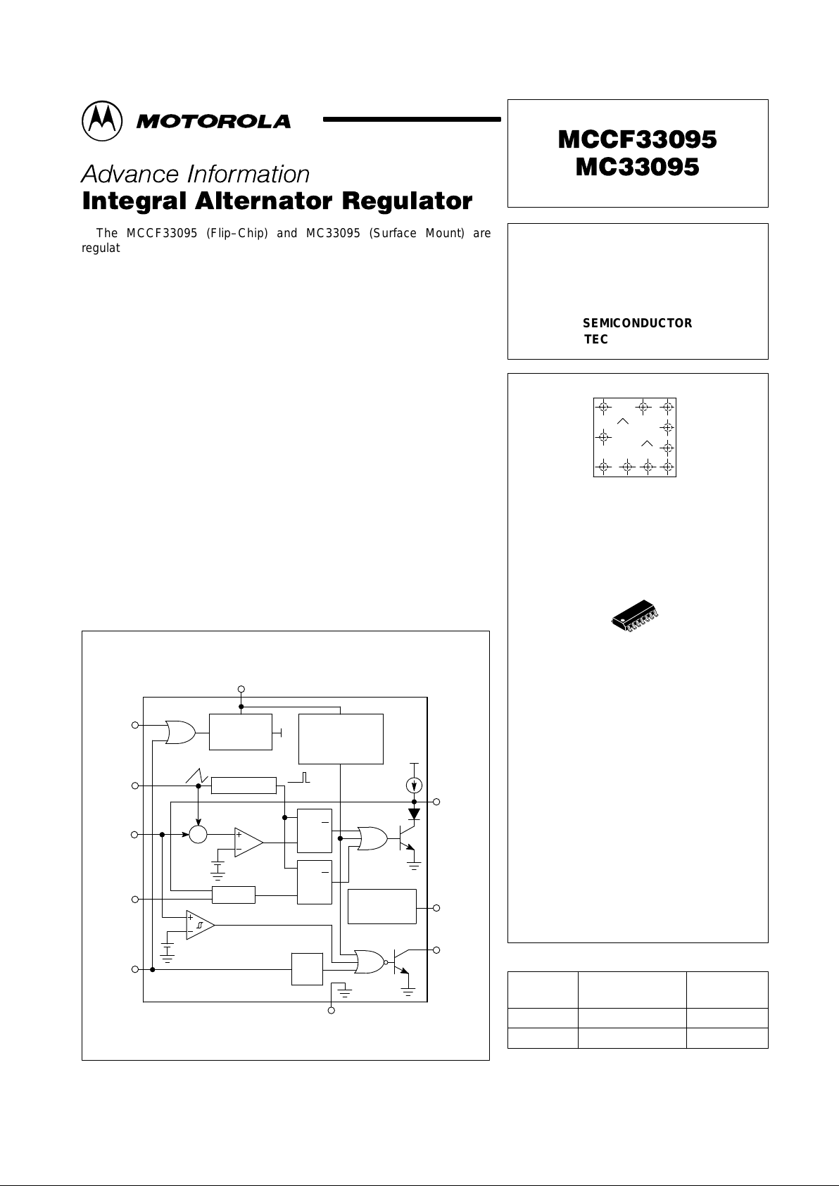
The MCCF33095 (Flip–Chip) and MC33095 (Surface Mount) are
regulator control integrated circuits designed for use in automotive 12 V
alternator charging systems. Few external components are required for full
system implementation. These devices provide control for a broad range of
12 V alternator charging systems when used in conjunction with the
appropriate Motorola Power Darlington transistor to control the field current
of the specific alternator.
Both versions have internal detection and protection features to withstand
extreme electrical variations encountered in harsh automotive environments.
Flip–Chip Technology allows the MCCF33095 to operate at higher ambient
temperatures than the surface mount version in addition to withstanding
severe vibration and thermal shock with a high degree of reliability.
• Constant Frequency with V ariable Duty Cycle Operation
• Adjusts System Charging to Compensate for Changes
in Ambient Temperature
• Slew Rate Control to Reduce EMI
• Lamp Pin to Indicate Abnormal Operating Conditions
• Shorted Field Protection
• Resumes Normal Operation Once Fault Condition Ceases
• Operation from –40°C to 170°C for Flip–Chip and –40°C to 125°C
for SO–14
• Surface Mount or Solder Bump Processed Flip–Chip Assembly Versions
Simplified Block Diagram
R
Q
S
V
CC
1 (12)
Darlington
Drive
Roll–Off
Lamp
9 (1)
V
Reg
Ground
8 (2)
Series
Regulator
Oscillator
Load Dump
Detection and
Protection
R
Q
S
Thermal
Protection
One
Shot
Timer
V
HV
4 (8)
Sense
Stator
Short
Circuit
Oscillator
Ignition
+
+
6 (4)
2 (11)
10 (14)
3 (10)
7 (3)
5 (5)
This device contains 145 active transistors.
This document contains information on a new product. Specifications and information herein
are subject to change without notice.
Motorola, Inc. 1996 Rev 1
MCCF33095 MC33095
2
MOTOROLA ANALOG IC DEVICE DATA
MAXIMUM RATINGS
(Notes 1 and 3)
Rating
Symbol Value Unit
Steady State VCC, V
IGN
, V
STA
– 9.0 to 24 V
VCC and V
IGN
Transient – 80 V
Bump Shear Strength (Flip–Chip) – 8.0 Grams/Bump
Thermal Characteristics (Thermal Resistance)
Junction–to–Substrate (Flip–Chip)
Junction–to–Ambient (SO–14)
R
θJS
R
θJA
29
145
°C/W
Junction Temperature
Flip–Chip
SO–14
T
J
170
150
°C
Operating Ambient Temperature Range
Flip–Chip
SO–14
T
A
–40 to +170
–40 to +125
°C
ELECTRICAL CHARACTERISTICS (Limit values are given for –40°C ≤ T
A
≤ 150°C (Flip–Chip), –40°C ≤ TA ≤ 125°C
(SO–14) and typical values represent approximate mean value at TA = 25°C. Oscillator, Roll–Of f, Ground, Short Circuit = 0 V,
and 12 V ≤ VCC, Sense, Stator, Ignition ≤ 16 V, unless otherwise specified.)
Characteristic
Symbol Min Typ Max Unit
SUPPL Y (VCC)
Supply Current I
CC
Disabled (Ignition = 0.5 V , Stator = 5.0 V) –50 0.2 300 µA
Enabled (VCC, Sense = 17 V , Ignition = 1.4 V) 0 3.9 25 mA
Darlington Drive Overvoltage V
Disable Threshold (VCC, Ignition, Short Circuit = 19 V to 29 V Ramp, Stator = 10 V) V
CODD
19 26 28.5
Hysteresis (VCC, Stator, Ignition, Short Circuit = 29 V to 19 V Ramp) V
CODDH
– 4.2 –
Lamp Overvoltage V
Disable Threshold (VCC, Stator, Ignition, Short Circuit = 19 V to 29 V Ramp) V
COL
19 22.3 29.5
Hysteresis V
COLH
– 0.3 –
SENSE
Sense Current (Oscillator = 2.0 V) I
SNS
–10 0.6 10 µA
Calibration Voltage (50% Duty Cycle) (Note 5) V
R
12.25 14.6 17.5 V
Lamp Comparator Detect Threshold V
SCD
– 16.3 – V
Proportional Control Range M
V
50 187.4 350 mV
Lamp Comparator Reset Threshold V
HV
15.4 15.9 16.4 V
Lamp Hysteresis V
HYS
20 416.6 600 mV
STATOR
Propagation Delay (Lamp–to–High, Stator = 15 V to 6.0 V) t
STA
6.0 59.4 600 ms
Reset Threshold Voltage (Lamp–to–Low, Stator = 5.0 V to 11 V) V
IH
6.0 8.8 11 V
Input Current (Sense = 18 V , Oscillator = 2.0 V) I
STA
–10 1.5 10 µA
LAMP
Saturation Voltage (Lamp = 14 mA) V
OLL
0 111.8 350 mV
Leakage Current (Sense = 1.0 V , Lamp = 2.5 V) I
OHL
–50 0.8 50 µA
Saturation Voltage (VCC, Sense, Stator, Ignition = 30 V, Lamp = 20 mA) V
OOLL
0 147.4 350 mV
NOTES: 1.VCC applied through a 250 Ω resistor.
2.Sense input applied through a 100 kΩ and 50 kΩ resistor divider to generate one–third V
bat
.
3.Stator and Ignition inputs applied through a 20 kΩ resistor.
4.Short Circuit input applied through a 30 kΩ resistor.
5.Oscillator pin connected in series with 0.022 µF capacitor to ground.
MCCF33095 MC33095
3
MOTOROLA ANALOG IC DEVICE DATA
ELECTRICAL CHARACTERISTICS (continued) (Limit values are given for –40°C ≤ T
A
≤ 150°C (Flip–Chip), –40°C ≤ TA ≤ 125°C
(SO–14) and typical values represent approximate mean value at TA = 25°C. Oscillator, Roll–Of f, Ground, Short Circuit = 0 V,
and 12 V ≤ VCC, Sense, Stator, Ignition ≤ 16 V, unless otherwise specified.)
DARLINGTON DRIVE
Source Current (Pins VCC, Sense, Ignition = 9.0 V , Darlington Drive = V across
Power Darlington)
I
OHDD
4.0 7.6 20 mA
Saturation Voltage (Sense = 18 V, Oscillator = 2.0 V, Darlington Drive = –100 µA) V
OLDD
0 300.1 350 mV
Minimum “On” Time (Sense = 18 V) (Note 5) t
DD
200 697.8 700 µs
Frequency (Note 5) F
OSC
75 174.7 325 Hz
Minimum Duty Cycle (Sense = 18 V) (Note 5) DC
DD
4.0 12.2 13 %
Rise Time (10% to 90%) (Note 5) t
r
10 21.4 50 µs
Fall Time (90% to 10%) (Note 5) t
f
10 23.7 50 µs
SHORT CIRCUIT
Duty Cycle (Note 5) DC
SC
1.0 1.7 5.0 %
“On” Time (Short Circuit High, Short Circuit = 8.0 V) (Note 5) PW
SC
60 99 660 µs
NOTES: 1.VCC applied through a 250 Ω resistor.
2.Sense input applied through a 100 kΩ and 50 kΩ resistor divider to generate one–third V
bat
.
3.Stator and Ignition inputs applied through a 20 kΩ resistor.
4.Short Circuit input applied through a 30 kΩ resistor.
5.Oscillator pin connected in series with 0.022 µF capacitor to ground.
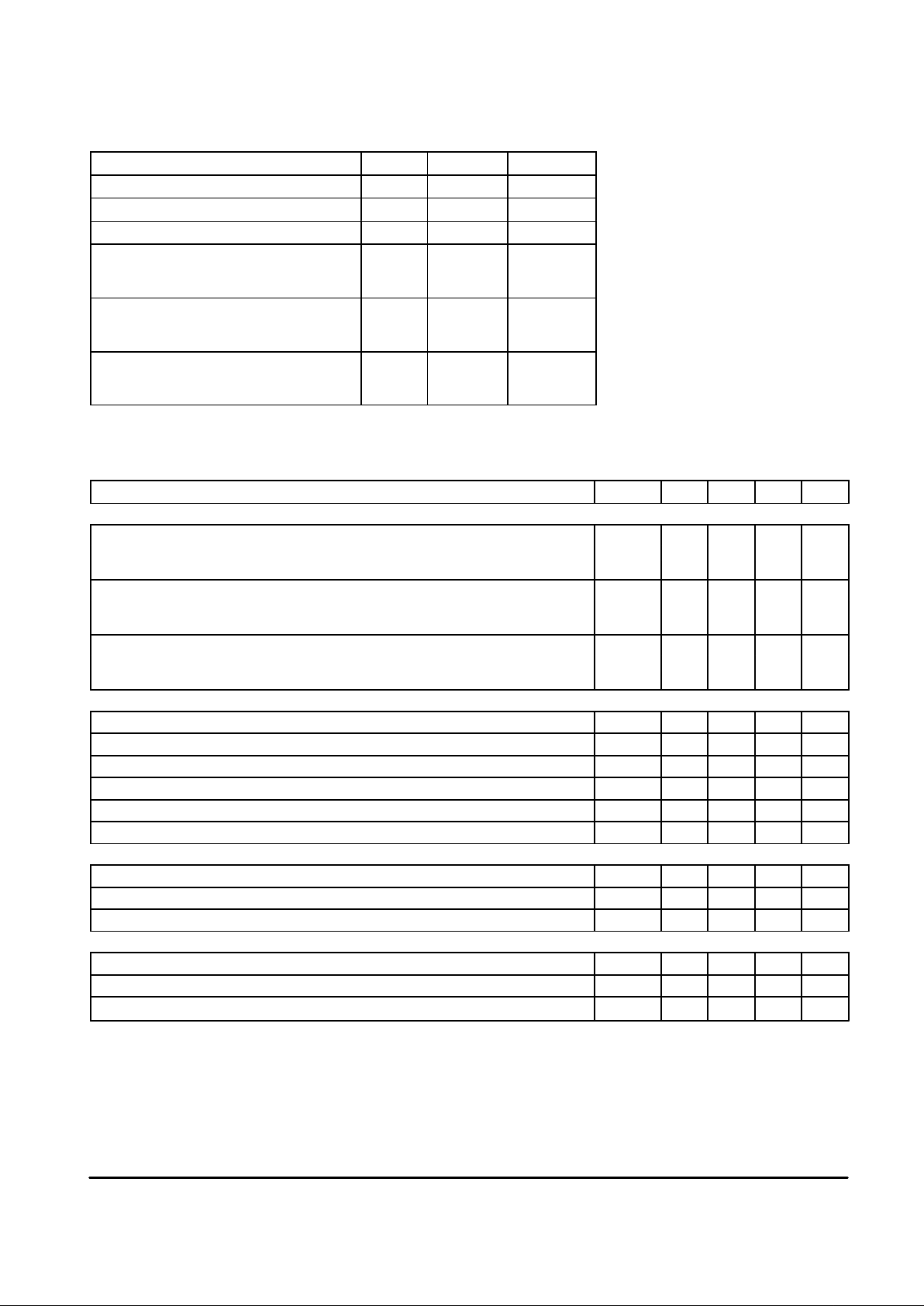
NOTES: 1.All dimensions shown indicated in millimeters.
2. Denotes basic dimension having zero
tolerance and describes the theoretical
exact location (true position) or contour.
–A–
Maximum taper either
direction allowed, 4 edges.
Die sawed through.
0.025R of True Position
0.140
0.050 10 Places
Dia. 10 Places
0.216
0.127
0.559
0.483
9
10
8
12
0
3
765
0
4
0.185
1.503
1.015
0.741
2.032
0
1.605
1.012
0.606
0.506
0.189
–B–
0.510
1.905
φ
Figure 1. Flip–Chip Mechanical Dimensions
0.029
MCCF33095 MC33095
4
MOTOROLA ANALOG IC DEVICE DATA
2.0
1.5
1.0
0.5
0
0
SC, CYCLE TIME (ms)
1.4 2.8 5.64.2
I
F
, FIELD CURRENT (A)
I
F
, FIELD CURRENT (A)
1.025
0
SC, CYCLE TIME (ms)
0.050
0
1.4 2.8 4.2 5.6
1.000
0.075
0.025
V
bat
, REQUIRED TO TURN–ON LAMP (V)
19
18
17
16
15
14
12.5
V
bat
FOR A 50% DUTY CYCLE (V)
13 13.5 14 14.5 15 16.515.5 16
Maximum Ratio (1.19)
Typical Ratio (1.13)
Minimum Ratio (1.08)
V
bat
, VOLTAGE FOR 50% DUTY CYCLE (V)
16.5
–40
TA, TEMPERATURE (
°
C)
15.0
14.0
13.0
12.5
0 40 80 120 160
16.0
15.5
14.5
13.5
Maximum
Minimum
Typical
0
t, TIME (ms)
0
100 300 400
80
60
40
20
200
V
LD
, TRANSIENT VOL TAGE (V)
40 60
V
40
t, TIME (ms)
–20
–75
420
20
–20
–40
–60
0 20 80 100 380 400
FT
, TRANSIENT FIELD VOLTAGE (V)
0
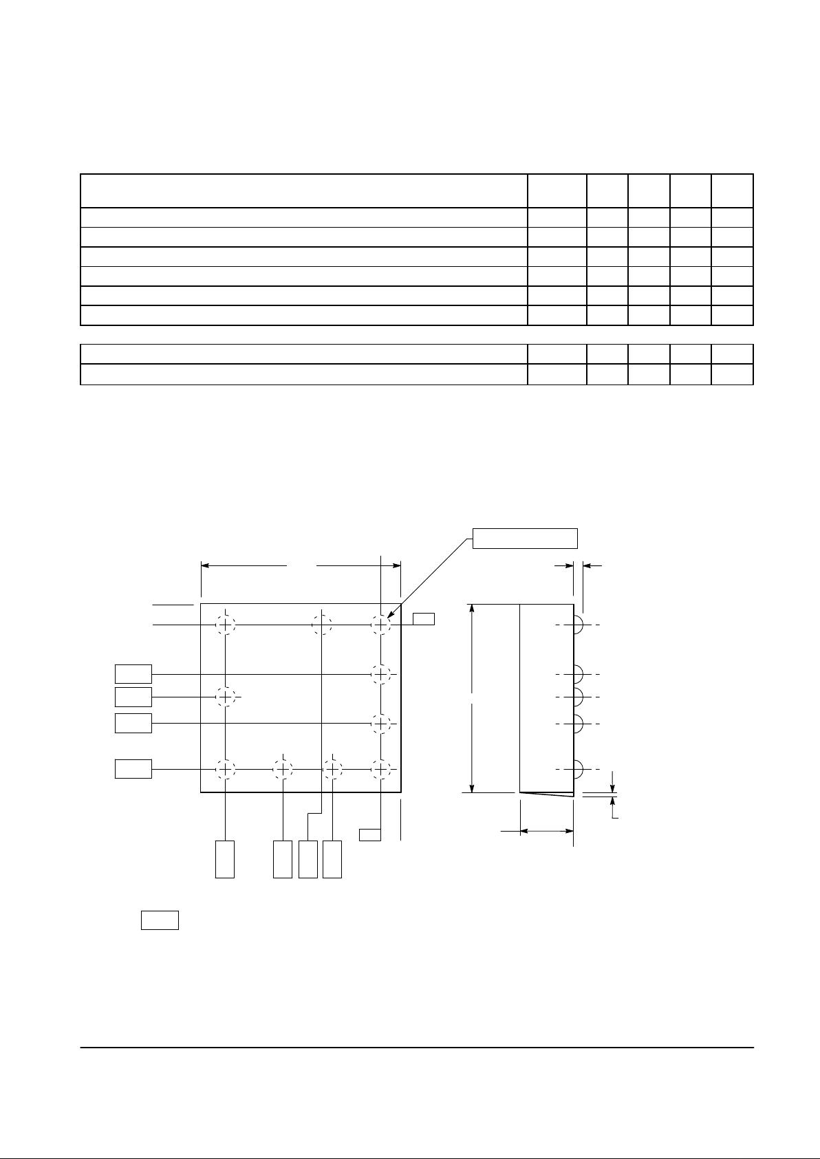
Figure 2. Pins 1, 3 and 4 Field Transient Decay Figure 3. Pins 1 and 4 Load Dump Transient Decay
Figure 4. Temperature versus
V
bat
for 50% Duty Cycle
Figure 5. V
bat
(50% Duty Cycle) versus
V
bat
(Lamp “On”)
Figure 6. Field Current versus Cycle Time Figure 7. Field Current versus Time
14.5 V
VFT = 14.5 V for 0 ≥ t ≥ 0.38 sec
VFT = – 75 e
t/0.038
for 0
≤
t ≤ 0.38 sec
Refer to Notes 1 to 5 of Electrical Table
for Circuit Hook–Up
VLD = 80 e
–5t
for 0 ≤ t ≤ 0.342 sec
VLD = 14.5 V for t
≥
0.342 sec
Refer to Notes 1 to 5 of Electrical
Table for Circuit Hook–Up
V
bat
= 14.4 V
Duty Cycle = 6.0%
TA = 25
°
C
V
bat
= 14.4 V
Duty Cycle = 86%
TA = 25
°
C
 Loading...