

Page 1

查询MC92501供应商
MOTOROLA
SEMICONDUCTOR TECHNICAL DATA
Order this document
by MC92501/D
MC92501
Advance Information
ATM Cell Processor
The ATM Cell Processor (MC92501) is an Asynchronous Transfer Mode (ATM)
layer device composed of dedicated high-performance ingress and egress cell
processors combined with UTOPIA Level 2-compliant physical (PHY) and switch
interface ports (see Block Diagram). The MC92501 is a second generation ATM
cell processor in MotorolaÕs 92500 series. This document provides information
on the new features offered by the second generation ATM cell processor. This
document, combined with MC92500/D, provides the complete speciÞcation for
the ATM cell processor.
GC SUFFIX
GTBGA
CASE 1208
New Features of the MC92501:
¥ Implements ATM Layer Functions for Broadband ISDN According to ATM
Forum UNI 4.0 and TM 4.0 SpeciÞcations, ITU Recommendations, and
Bellcore Recommendations
¥ Provides ABR Relative Rate Marking and EFCI Marking According to TM 4.0
¥ Selective Discard CLP = 1 (or CLP = 0+1) Flow on Selected Connections
¥ UTOPIA Level 2 PHY Interface and UTOPIA ATM Layer Interface
¥ Supports Both Partial Packet Discard (PPD) and Early Packet Discard (EPD)
¥ Change ABR RM Cell Priority
¥ Support for CLP Transparency
Existing MC92500 Features:
¥ Full-Duplex Operation at Data Rates up to 155 Mbit/sec
¥ Performs Internal VPI and VCI Address Compression for up to 64K VCs
¥ CLP-Aware Peak, Average, and Burst-Length Policing with Programmable
Tag/Drop Action Per Policer
¥ Supports up to 16 Physical Links Using Dedicated Ingress/Egress MultiPHY
Control Signals
¥ Each Physical Link Can Be ConÞgured as Either a UNI or NNI Port
¥ Supports Multicast, Multiport Address Translation
¥ Maintains Both Virtual Connection and Physical Link Counters on Both
Ingress and Egress Cell Flows
¥ Provides a Flexible 32-Bit External Memory Port for Context Management
¥ Automated AIS, RDI, CC, and Loopback Functions with Performance
Monitoring Block Test on All 64K Connections
¥ Programmable 32-Bit Microprocessor Interface Supporting Big-Endian or
Little-Endian Bus Formats
¥ Bidirectional UPC or NPC Design with up to Four Leaky Buckets Per
Connection
¥ Supports a Programmable Number of Additional Switch Overhead
Parameters Allowing Adaptation to Any Switch Routing Header Format
¥ Provides Per-Link Cell Counters in Both Directions
ORDERING INFORMATION
MC92501GC GTBGA
This document contains information on a new product. SpeciÞcations and information herein are subject to change without notice.
REV 1.2
2/98 TN98020500
© Motorola, Inc. 1998
MOTOROLA
MC92501
1
Page 2
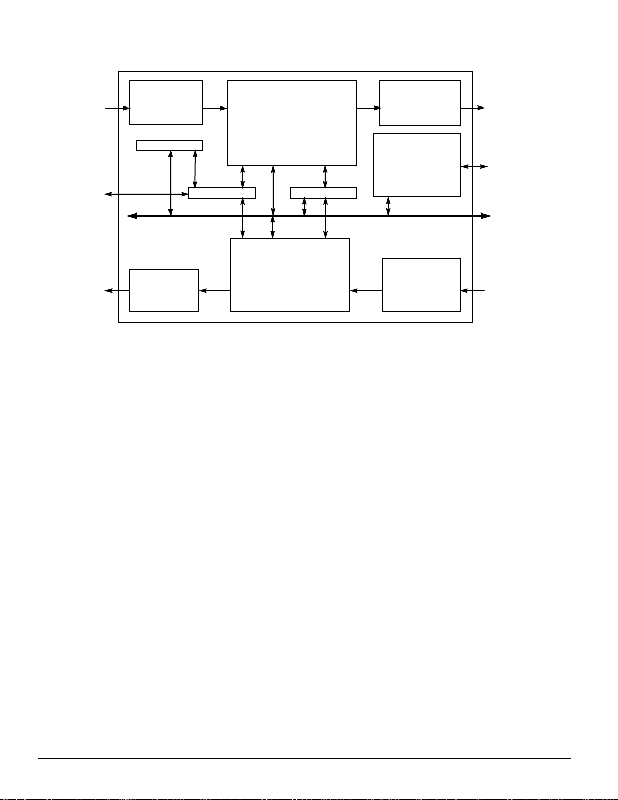
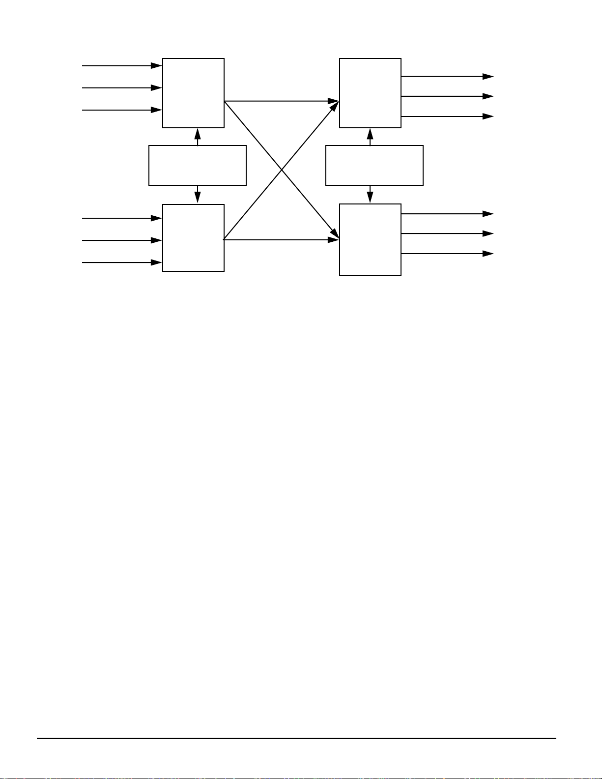
REPRESENTATIVE BLOCK DIAGRAM
UTOPIA IF
EXTERNAL
MEMORY IF
UTOPIA IF
INGRESS PHY IF
CRC Check (OAM)
MultiPHY Support
INTERNAL SCAN
EGRESS PHY IF
CRC Gen (OAM)
MultiPHY Support
Microprocessor Cell Insertion/Extraction
EXT MEMORY IF
Microprocessor Cell Insertion/Extraction
INGRESS CELL PROCESSOR
VP and VC Address Translation
NPC/UPC
Cell Counting
OAM Operations
Add Switch Parameters
FMC GENERATION
EGRESS CELL PROCESSOR
Multicast Translation
Cell Counting
OAM Operations
Address Translation
INGRESS SWITCH IF
CRC Generation
Independent Clock
MICROPROCESSOR IF
Cell Insertion
Cell Extraction
ConÞg Registers
Maintenance Access
EGRESS SWITCH IF
Extract Overhead
CRC Check
Independent Clock
UTOPIA IF
MICROPROCESSOR IF
UTOPIA IF
MC92501
2
MOTOROLA
Page 3

TABLE OF CONTENTS
SECTION 1. ATM NETWORK . . . . . . . . . . . . . . . . . . . . . . . . . . . . . . . . . . . . . . . . . . . . . . . . . . . . . . . . . . . . . . 5
1.1. ATM Network Description . . . . . . . . . . . . . . . . . . . . . . . . . . . . . . . . . . . . . . . . . . . . . . . . . . . . . . . . . . . . . . . . . . . . . . .5
1.2. ATM Network Applications . . . . . . . . . . . . . . . . . . . . . . . . . . . . . . . . . . . . . . . . . . . . . . . . . . . . . . . . . . . . . . . . . . . . . . . 6
SECTION 2. FUNCTIONAL DESCRIPTION . . . . . . . . . . . . . . . . . . . . . . . . . . . . . . . . . . . . . . . . . . . . . . . . . . . 7
2.1. System Functional Description . . . . . . . . . . . . . . . . . . . . . . . . . . . . . . . . . . . . . . . . . . . . . . . . . . . . . . . . . . . . . . . . . . . . 7
2.2. MC92501 Functional Description . . . . . . . . . . . . . . . . . . . . . . . . . . . . . . . . . . . . . . . . . . . . . . . . . . . . . . . . . . . . . . . . . . 7
2.3. First Generation Features . . . . . . . . . . . . . . . . . . . . . . . . . . . . . . . . . . . . . . . . . . . . . . . . . . . . . . . . . . . . . . . . . . . . . . . 7
SECTION 3. PACKET-BASED UPC Discard Algorithms . . . . . . . . . . . . . . . . . . . . . . . . . . . . . . . . . . . . . . . . 8
3.1. Introduction . . . . . . . . . . . . . . . . . . . . . . . . . . . . . . . . . . . . . . . . . . . . . . . . . . . . . . . . . . . . . . . . . . . . . . . . . . . . . . . . . .8
3.1.1. AAL5 Packet Definition . . . . . . . . . . . . . . . . . . . . . . . . . . . . . . . . . . . . . . . . . . . . . . . . . . . . . . . . . . . . . . . . . . . . . . . . .8
3.2. Cell-Based UPC . . . . . . . . . . . . . . . . . . . . . . . . . . . . . . . . . . . . . . . . . . . . . . . . . . . . . . . . . . . . . . . . . . . . . . . . . . . . . . . 8
3.3. Partial Packet Discard (PPD) . . . . . . . . . . . . . . . . . . . . . . . . . . . . . . . . . . . . . . . . . . . . . . . . . . . . . . . . . . . . . . . . . . . . . 8
3.4. Early Packet Discard (EPD) . . . . . . . . . . . . . . . . . . . . . . . . . . . . . . . . . . . . . . . . . . . . . . . . . . . . . . . . . . . . . . . . . . . . . . 9
3.5. Limited Early Packet Discard (Limited EPD) . . . . . . . . . . . . . . . . . . . . . . . . . . . . . . . . . . . . . . . . . . . . . . . . . . . . . . . . . 9
SECTION 4. SELECTIVE DISCARD . . . . . . . . . . . . . . . . . . . . . . . . . . . . . . . . . . . . . . . . . . . . . . . . . . . . . . . . 11
SECTION 5. Available Bit Rate (ABR) Support. . . . . . . . . . . . . . . . . . . . . . . . . . . . . . . . . . . . . . . . . . . . . . . 12
5.1. Overview and Features . . . . . . . . . . . . . . . . . . . . . . . . . . . . . . . . . . . . . . . . . . . . . . . . . . . . . . . . . . . . . . . . . . . . . . . . 12
5.2. RM Cell Definition . . . . . . . . . . . . . . . . . . . . . . . . . . . . . . . . . . . . . . . . . . . . . . . . . . . . . . . . . . . . . . . . . . . . . . . . . . . .12
5.3. RM Cell Fields . . . . . . . . . . . . . . . . . . . . . . . . . . . . . . . . . . . . . . . . . . . . . . . . . . . . . . . . . . . . . . . . . . . . . . . . . . . . . . . 12
5.4. Cell Marking (CI, NI, PTI) . . . . . . . . . . . . . . . . . . . . . . . . . . . . . . . . . . . . . . . . . . . . . . . . . . . . . . . . . . . . . . . . . . . . . . . 13
5.4.1. Sources for Ingress Flow Status . . . . . . . . . . . . . . . . . . . . . . . . . . . . . . . . . . . . . . . . . . . . . . . . . . . . . . . . . . . . . . . . . 14
5.4.1.1. Ingress Flow Status from Global Register . . . . . . . . . . . . . . . . . . . . . . . . . . . . . . . . . . . . . . . . . . . . . . . . . . . . . . . . . . 14
5.4.1.2. Ingress Flow Status from CellÕs Overhead . . . . . . . . . . . . . . . . . . . . . . . . . . . . . . . . . . . . . . . . . . . . . . . . . . . . . . . . . . 14
5.4.1.3. Ingress Flow Status from Context Memory . . . . . . . . . . . . . . . . . . . . . . . . . . . . . . . . . . . . . . . . . . . . . . . . . . . . . . . . . 14
5.4.1.4. Logic of Ingress Flow Status . . . . . . . . . . . . . . . . . . . . . . . . . . . . . . . . . . . . . . . . . . . . . . . . . . . . . . . . . . . . . . . . . . . . 14
5.4.2. Sources for Egress Flow Status . . . . . . . . . . . . . . . . . . . . . . . . . . . . . . . . . . . . . . . . . . . . . . . . . . . . . . . . . . . . . . . . . . 14
5.4.2.1. Egress Flow Status from Global Register . . . . . . . . . . . . . . . . . . . . . . . . . . . . . . . . . . . . . . . . . . . . . . . . . . . . . . . . . . 14
5.4.2.2. Egress Flow Status from CellÕs Overhead . . . . . . . . . . . . . . . . . . . . . . . . . . . . . . . . . . . . . . . . . . . . . . . . . . . . . . . . . .14
5.4.2.3. Egress Flow Status from Context Memory . . . . . . . . . . . . . . . . . . . . . . . . . . . . . . . . . . . . . . . . . . . . . . . . . . . . . . . . . . 15
5.4.2.4. Logic of Egress Flow Status . . . . . . . . . . . . . . . . . . . . . . . . . . . . . . . . . . . . . . . . . . . . . . . . . . . . . . . . . . . . . . . . . . . . . 15
5.4.3. Ingress ABR Marking Bits . . . . . . . . . . . . . . . . . . . . . . . . . . . . . . . . . . . . . . . . . . . . . . . . . . . . . . . . . . . . . . . . . . . . . . 15
5.4.3.1. Logic of Ingress ABR Marking Bits . . . . . . . . . . . . . . . . . . . . . . . . . . . . . . . . . . . . . . . . . . . . . . . . . . . . . . . . . . . . . . . . 15
5.4.4. Egress ABR Marking Bits . . . . . . . . . . . . . . . . . . . . . . . . . . . . . . . . . . . . . . . . . . . . . . . . . . . . . . . . . . . . . . . . . . . . . . . 15
5.4.4.1. Logic of Egress ABR Marking Bits . . . . . . . . . . . . . . . . . . . . . . . . . . . . . . . . . . . . . . . . . . . . . . . . . . . . . . . . . . . . . . . . 16
5.4.5. Cell Marking Examples . . . . . . . . . . . . . . . . . . . . . . . . . . . . . . . . . . . . . . . . . . . . . . . . . . . . . . . . . . . . . . . . . . . . . . . .16
5.5. Ingress Switch ABR Priority Interface . . . . . . . . . . . . . . . . . . . . . . . . . . . . . . . . . . . . . . . . . . . . . . . . . . . . . . . . . . . . . 18
5.5.1. An Example . . . . . . . . . . . . . . . . . . . . . . . . . . . . . . . . . . . . . . . . . . . . . . . . . . . . . . . . . . . . . . . . . . . . . . . . . . . . . . . . . 18
5.6. Egress Reset EFCI . . . . . . . . . . . . . . . . . . . . . . . . . . . . . . . . . . . . . . . . . . . . . . . . . . . . . . . . . . . . . . . . . . . . . . . . . . .18
SECTION 6. CLP TRANSPARENCY. . . . . . . . . . . . . . . . . . . . . . . . . . . . . . . . . . . . . . . . . . . . . . . . . . . . . . . . 19
6.1. Overview . . . . . . . . . . . . . . . . . . . . . . . . . . . . . . . . . . . . . . . . . . . . . . . . . . . . . . . . . . . . . . . . . . . . . . . . . . . . . . . . . . . 19
SECTION 7. INDIRECT EXTERNAL MEMORY ACCESS . . . . . . . . . . . . . . . . . . . . . . . . . . . . . . . . . . . . . . . 20
7.1. Overview . . . . . . . . . . . . . . . . . . . . . . . . . . . . . . . . . . . . . . . . . . . . . . . . . . . . . . . . . . . . . . . . . . . . . . . . . . . . . . . . . . . 20
7.2. User Interface . . . . . . . . . . . . . . . . . . . . . . . . . . . . . . . . . . . . . . . . . . . . . . . . . . . . . . . . . . . . . . . . . . . . . . . . . . . . . . . . 20
7.2.1. Write Access . . . . . . . . . . . . . . . . . . . . . . . . . . . . . . . . . . . . . . . . . . . . . . . . . . . . . . . . . . . . . . . . . . . . . . . . . . . . . . . . 20
7.2.2. Read Access . . . . . . . . . . . . . . . . . . . . . . . . . . . . . . . . . . . . . . . . . . . . . . . . . . . . . . . . . . . . . . . . . . . . . . . . . . . . . . . . 20
SECTION 8. IMPROVED HOST INTERFACE . . . . . . . . . . . . . . . . . . . . . . . . . . . . . . . . . . . . . . . . . . . . . . . . . 21
8.1. Overview . . . . . . . . . . . . . . . . . . . . . . . . . . . . . . . . . . . . . . . . . . . . . . . . . . . . . . . . . . . . . . . . . . . . . . . . . . . . . . . . . . . 21
8.1.1. An Additional MDTACK Signal . . . . . . . . . . . . . . . . . . . . . . . . . . . . . . . . . . . . . . . . . . . . . . . . . . . . . . . . . . . . . . . . . . . 21
8.1.2. Programmable MREQ Signals . . . . . . . . . . . . . . . . . . . . . . . . . . . . . . . . . . . . . . . . . . . . . . . . . . . . . . . . . . . . . . . . . . . 21
8.1.3. Update the Definition of MWSH and MWSL Signals . . . . . . . . . . . . . . . . . . . . . . . . . . . . . . . . . . . . . . . . . . . . . . . . . . 21
SECTION 9. EGRESS OVERHEAD MANIPULATION . . . . . . . . . . . . . . . . . . . . . . . . . . . . . . . . . . . . . . . . . . 22
SECTION 10. UTOPIA LEVEL 2 PHY INTERFACE . . . . . . . . . . . . . . . . . . . . . . . . . . . . . . . . . . . . . . . . . . . . . 23
SECTION 11. Register Descriptions . . . . . . . . . . . . . . . . . . . . . . . . . . . . . . . . . . . . . . . . . . . . . . . . . . . . . . . . 24
11.1. General Register List . . . . . . . . . . . . . . . . . . . . . . . . . . . . . . . . . . . . . . . . . . . . . . . . . . . . . . . . . . . . . . . . . . . . . . . . . .24
11.2. Status Reporting Registers . . . . . . . . . . . . . . . . . . . . . . . . . . . . . . . . . . . . . . . . . . . . . . . . . . . . . . . . . . . . . . . . . . . . . 24
11.2.1. Interrupt Register (IR) . . . . . . . . . . . . . . . . . . . . . . . . . . . . . . . . . . . . . . . . . . . . . . . . . . . . . . . . . . . . . . . . . . . . . . . . .24
11.2.2. Interrupt Mask Register (IMR) . . . . . . . . . . . . . . . . . . . . . . . . . . . . . . . . . . . . . . . . . . . . . . . . . . . . . . . . . . . . . . . . . . . 24
11.2.3. ATMC CFB Revision Register (ARR) . . . . . . . . . . . . . . . . . . . . . . . . . . . . . . . . . . . . . . . . . . . . . . . . . . . . . . . . . . . . . . 25
MOTOROLA
MC92501
3
Page 4

TABLE OF CONTENTS (CONTINUED)
11.2.4. MC92501 Revision Register (RR) . . . . . . . . . . . . . . . . . . . . . . . . . . . . . . . . . . . . . . . . . . . . . . . . . . . . . . . . . . . . . . . . 25
11.3. Control Registers . . . . . . . . . . . . . . . . . . . . . . . . . . . . . . . . . . . . . . . . . . . . . . . . . . . . . . . . . . . . . . . . . . . . . . . . . . . . 25
11.3.1. Ingress Processing Control Register (IPLR) . . . . . . . . . . . . . . . . . . . . . . . . . . . . . . . . . . . . . . . . . . . . . . . . . . . . . . . . 25
11.3.2. Egress Processing Control Register (EPLR) . . . . . . . . . . . . . . . . . . . . . . . . . . . . . . . . . . . . . . . . . . . . . . . . . . . . . . . 25
11.3.3. Indirect External Memory Access Address Register (IAAR) . . . . . . . . . . . . . . . . . . . . . . . . . . . . . . . . . . . . . . . . . . . . 26
11.3.4. Indirect External Memory Access Data Register (IADR) . . . . . . . . . . . . . . . . . . . . . . . . . . . . . . . . . . . . . . . . . . . . . . 26
11.4. Configuration Register . . . . . . . . . . . . . . . . . . . . . . . . . . . . . . . . . . . . . . . . . . . . . . . . . . . . . . . . . . . . . . . . . . . . . . . . 27
11.4.1. Ingress Processing Configuration Register (IPCR) . . . . . . . . . . . . . . . . . . . . . . . . . . . . . . . . . . . . . . . . . . . . . . . . . . . 27
11.4.2. Egress Processing Configuration Register (EPCR) . . . . . . . . . . . . . . . . . . . . . . . . . . . . . . . . . . . . . . . . . . . . . . . . . . 28
11.4.3. ATMC CFB Configuration Register (ACR) . . . . . . . . . . . . . . . . . . . . . . . . . . . . . . . . . . . . . . . . . . . . . . . . . . . . . . . . . 29
11.4.4. Egress Switch Interface Configuration Register (ESWCR) . . . . . . . . . . . . . . . . . . . . . . . . . . . . . . . . . . . . . . . . . . . . . 29
11.4.5. Egress Switch Overhead Information Register 0 (ESOIR0) . . . . . . . . . . . . . . . . . . . . . . . . . . . . . . . . . . . . . . . . . . . . 30
11.4.6. Microprocessor Configuration Register (MPCONR) . . . . . . . . . . . . . . . . . . . . . . . . . . . . . . . . . . . . . . . . . . . . . . . . . . 30
11.4.7. Maintenance Configuration Register (MACONR) . . . . . . . . . . . . . . . . . . . . . . . . . . . . . . . . . . . . . . . . . . . . . . . . . . . . 31
11.4.8. Ingress PHY Configuration Register (IPHCR) . . . . . . . . . . . . . . . . . . . . . . . . . . . . . . . . . . . . . . . . . . . . . . . . . . . . . . 31
11.4.9. Egress PHY Configuration Register (EPHCR) . . . . . . . . . . . . . . . . . . . . . . . . . . . . . . . . . . . . . . . . . . . . . . . . . . . . . . 31
11.4.10. MC92501 General Configuration Register (GCR) . . . . . . . . . . . . . . . . . . . . . . . . . . . . . . . . . . . . . . . . . . . . . . . . . . . 32
11.4.11. Egress Switch Overhead Information Register 1 (ESOIR1) . . . . . . . . . . . . . . . . . . . . . . . . . . . . . . . . . . . . . . . . . . . . 32
11.4.12. RM Overlay Register (RMOR) . . . . . . . . . . . . . . . . . . . . . . . . . . . . . . . . . . . . . . . . . . . . . . . . . . . . . . . . . . . . . . . . . . 33
11.4.13. CLP Transparency Overlay Register (CTOR) . . . . . . . . . . . . . . . . . . . . . . . . . . . . . . . . . . . . . . . . . . . . . . . . . . . . . . . 33
11.4.14. Context Parameters Extension Table Pointer Register (CPETP) . . . . . . . . . . . . . . . . . . . . . . . . . . . . . . . . . . . . . . . . 33
11.4.15. Egress Overhead Manipulation Register (EGOMR) . . . . . . . . . . . . . . . . . . . . . . . . . . . . . . . . . . . . . . . . . . . . . . . . . . 34
SECTION 12. EXTERNAL MEMORY DESCRIPTION . . . . . . . . . . . . . . . . . . . . . . . . . . . . . . . . . . . . . . . . . . . . 35
12.1. Context Parameters Extension Table . . . . . . . . . . . . . . . . . . . . . . . . . . . . . . . . . . . . . . . . . . . . . . . . . . . . . . . . . . . . . 35
12.1.1. Common Parameters Extension Word . . . . . . . . . . . . . . . . . . . . . . . . . . . . . . . . . . . . . . . . . . . . . . . . . . . . . . . . . . . . 35
12.2. CONTEXT PARAMETERS TABLE . . . . . . . . . . . . . . . . . . . . . . . . . . . . . . . . . . . . . . . . . . . . . . . . . . . . . . . . . . . . . . . 36
12.2.1. Egress Parameters . . . . . . . . . . . . . . . . . . . . . . . . . . . . . . . . . . . . . . . . . . . . . . . . . . . . . . . . . . . . . . . . . . . . . . . . . . . 36
12.2.2. Ingress Parameters: . . . . . . . . . . . . . . . . . . . . . . . . . . . . . . . . . . . . . . . . . . . . . . . . . . . . . . . . . . . . . . . . . . . . . . . . . . 36
12.2.3. Common Parameters . . . . . . . . . . . . . . . . . . . . . . . . . . . . . . . . . . . . . . . . . . . . . . . . . . . . . . . . . . . . . . . . . . . . . . . . . 37
SECTION 13. DATA STRUCTURES . . . . . . . . . . . . . . . . . . . . . . . . . . . . . . . . . . . . . . . . . . . . . . . . . . . . . . . . . 38
13.1. General Fields . . . . . . . . . . . . . . . . . . . . . . . . . . . . . . . . . . . . . . . . . . . . . . . . . . . . . . . . . . . . . . . . . . . . . . . . . . . . . . . 38
13.1.1. Reason . . . . . . . . . . . . . . . . . . . . . . . . . . . . . . . . . . . . . . . . . . . . . . . . . . . . . . . . . . . . . . . . . . . . . . . . . . . . . . . . . . . . 38
SECTION 14. SIGNAL DESCRIPTION . . . . . . . . . . . . . . . . . . . . . . . . . . . . . . . . . . . . . . . . . . . . . . . . . . . . . . . 39
14.1. Microproccessor Signals (MP) . . . . . . . . . . . . . . . . . . . . . . . . . . . . . . . . . . . . . . . . . . . . . . . . . . . . . . . . . . . . . . . . . . 39
14.2. Ingress PHY Signals . . . . . . . . . . . . . . . . . . . . . . . . . . . . . . . . . . . . . . . . . . . . . . . . . . . . . . . . . . . . . . . . . . . . . . . . . . 40
14.3. Egress PHY Signals . . . . . . . . . . . . . . . . . . . . . . . . . . . . . . . . . . . . . . . . . . . . . . . . . . . . . . . . . . . . . . . . . . . . . . . . . . 40
SECTION 15. TEST OPERATION . . . . . . . . . . . . . . . . . . . . . . . . . . . . . . . . . . . . . . . . . . . . . . . . . . . . . . . . . . . 41
15.1. Device Identification Register . . . . . . . . . . . . . . . . . . . . . . . . . . . . . . . . . . . . . . . . . . . . . . . . . . . . . . . . . . . . . . . . . . . 41
15.2. Boundary Scan Register . . . . . . . . . . . . . . . . . . . . . . . . . . . . . . . . . . . . . . . . . . . . . . . . . . . . . . . . . . . . . . . . . . . . . . . 41
SECTION 16. Electrical Characteristics . . . . . . . . . . . . . . . . . . . . . . . . . . . . . . . . . . . . . . . . . . . . . . . . . . . . . 47
16.1. Electrical Specification for Clocks and Interfaces . . . . . . . . . . . . . . . . . . . . . . . . . . . . . . . . . . . . . . . . . . . . . . . . . . . . 47
16.2. DC Electrical Characteristics . . . . . . . . . . . . . . . . . . . . . . . . . . . . . . . . . . . . . . . . . . . . . . . . . . . . . . . . . . . . . . . . . . . 47
SECTION 17. Packaging Information. . . . . . . . . . . . . . . . . . . . . . . . . . . . . . . . . . . . . . . . . . . . . . . . . . . . . . . . 48
17.1. Additional Pins . . . . . . . . . . . . . . . . . . . . . . . . . . . . . . . . . . . . . . . . . . . . . . . . . . . . . . . . . . . . . . . . . . . . . . . . . . . . . . 48
17.2. Pin Assignment . . . . . . . . . . . . . . . . . . . . . . . . . . . . . . . . . . . . . . . . . . . . . . . . . . . . . . . . . . . . . . . . . . . . . . . . . . . . . . 48
17.3. 256-Lead GTBGA Outline . . . . . . . . . . . . . . . . . . . . . . . . . . . . . . . . . . . . . . . . . . . . . . . . . . . . . . . . . . . . . . . . . . . . . . 49
MC92501
4
MOTOROLA
Page 5
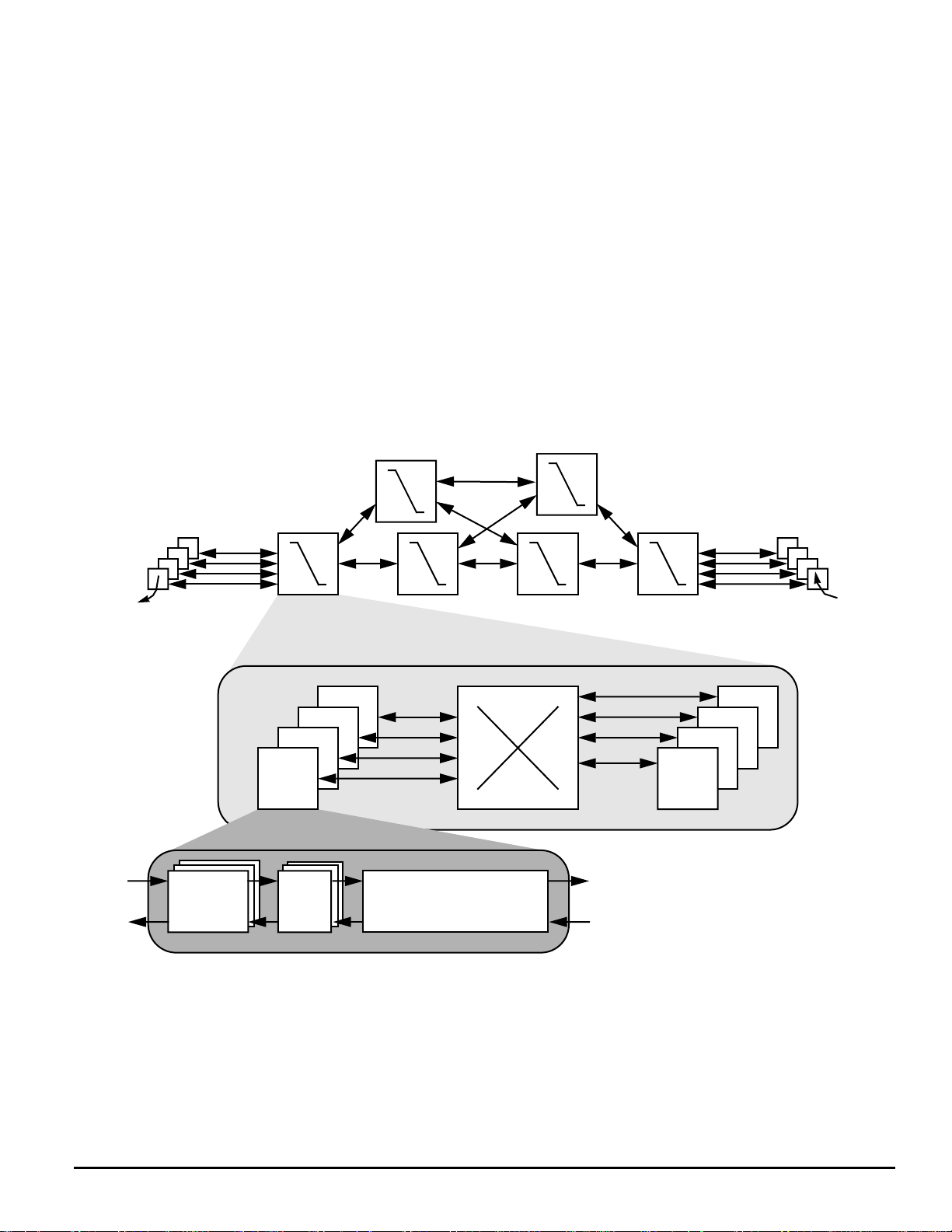
SECTION 1. ATM NETWORK
1.1. ATM Network Description
A typical ATM network consists of user end stations that
transmit and receive 53-byte data cells on virtual connections
(see Figure 1). Physical links and switching systems
interconnect the virtual connections. A virtual connectionÕs
path is established at the beginning of the data transfer,
maintained while the end-stations are communicating, and
torn down after the transfer is complete. This transmission
method increases the transfer speed because the
determination of the path the data will take is done only at the
beginning of the data transfer instead of when each data subblock or packet is transferred.
On a given physical link, each connection is assigned a
unique connection identiÞer. The connection identiÞer is
placed in the header of each cell by the transmitting equipment
and is used by the receiving equipment to route the cell to the
next physical link on the connection path. All cells belonging
to a speciÞc virtual connection follow the identical path from
VCs
Switch
the transmitting end station through the switching systems to
the receiving end station.
An ATM switch contains a high-speed switching fabric that
connects multiple line cards. The switching fabric connects the
input port to the output port based on the switchÕs routing table.
The line card interfaces between the physical medium and the
switching fabric by recovering incoming cells from the arriving
bit stream or converting outgoing cells into a bit stream for
transmission. An ATM swtich partitioned in this fashion can
efÞciently handle multiple physical links by independently
transferring each incoming ATM cell from its source port to its
destination port, based on the switchÕs routing table.
ATM standards divide the tasks to be performed on each
side of the switch fabric into PHY layer and ATM layer tasks.
The PHY layer tasks are dependent on the physical medium
that connects ATM switches. The ATM layer tasks operate at
the cell level and are independent of the physical medium.
Switch
VCs
END STATIONS
SWITCH
CLK REC
Switch
LINE
CARD
PHY
Switch Switch Switch
SWITCHING FABRIC
MC92501
ATM LAYER FUNCTIONS
Figure 1. MC92501 in an ATM Network Application
END STATIONS
LINE
CARD
LINE CARD
MOTOROLA
MC92501
5
Page 6
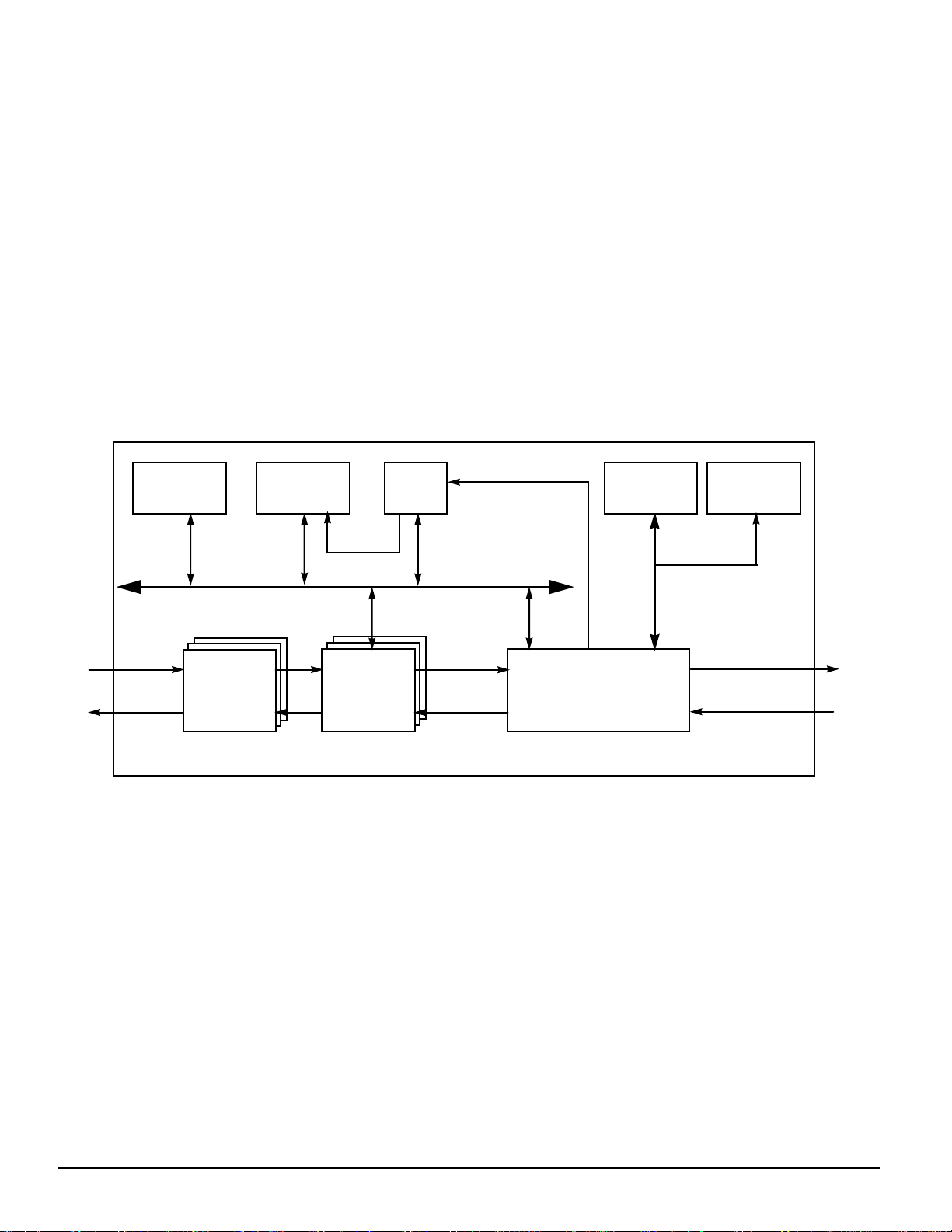
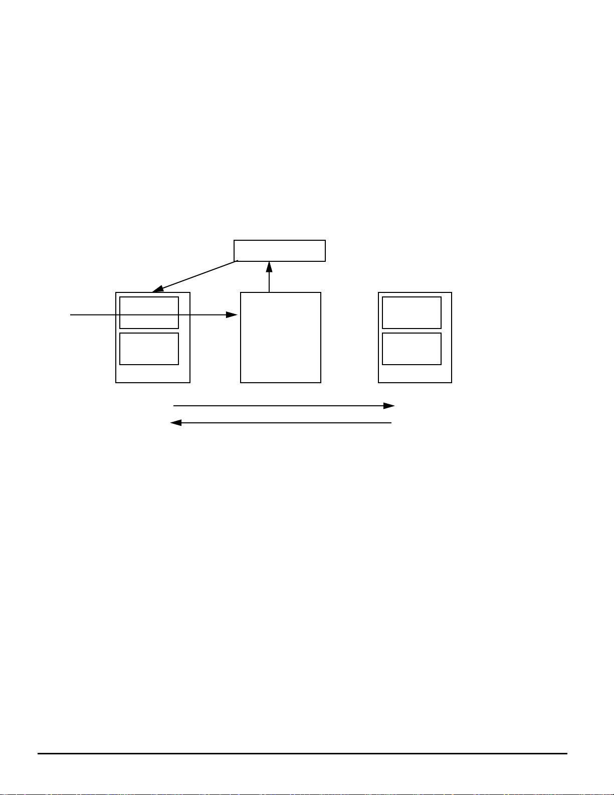
1.2. ATM Network Applications
The MC92501 performs the ATM layer functions in an ATM
switch such as cell processing and routing. Since the
MC92501 is an ATM layer device, it is PHY layer independent.
Figure 2 illustrates a typical ATM line card. The MC92501
uses an external memory for storing the cells that it
processes. In addition, the MC92501 offers an option to utilize
an external address compression device accessed via the
same external memory bus.
The microprocessor is used for conÞguration, control, and
status monitoring of the MC92501 and is responsible for
initializing and maintaining the external memory. The
MC92501 is the master of the external memory bus. At regular
intervals, the MC92501 allows the microprocessor to access
the external memory for updating and maintenance.
System RAM can also be located on the line card. The
MC92501 can support a DMA device to allow efÞcient data
transfer to this RAM without processor intervention.
RAM
MICRO-
PROCESSOR
DMA
DMA
The physical interface (PHY-IF) implements the physical
layer functions of the B-ISDN Protocol Reference Model. This
includes the physical medium dependent functions required
to transport ATM cells between the ATM user and the ATM
switch (UNI) or between two ATM switches (NNI). The cells
are transferred between the physical interface and the
MC92501 using the UTOPIA Level 2 standard.
The MC92501 implements B-ISDN UNI/NNI ATM layer
functions required to transfer cells to and from the switch over
virtual connections. These functions include usage
enforcement, address translation, and Operation,
Administration, and Maintenance (OAM) processing. The
MC92501 provides context management for up to 65,536
(64K) Virtual Connections (VCs). The VCs can be either Virtual
Path Connections (VPCs) or Virtual Channel Connections
(VCCs). ATM cells belonging to a particular VCC on a logical
link have the same unique Virtual Path IdentiÞer/Virtual
Channel IdentiÞer (VPI/VCI) value in the cell header. Similarly,
cells belonging to a particular VPC on the same logical link
share a unique VPI.
EXTERNAL
MEMORY
EXTERNAL
ADDRESS
COMPRESSION
MICROPROCESSOR BUS
RECOVERY
LINE CARD
CLOCK
PHY-IF
PHY-IF
PHY IF
MC92501
Figure 2. Typical MC92501 Line Card Application
EXTERNAL
MEMORY
BUS
TO SWITCH
FROM SWITCH
MC92501
6
MOTOROLA
Page 7

SECTION 2. FUNCTIONAL DESCRIPTION
2.1. System Functional Description
A serial transmission link operating at up to 155.52 Mbit/sec
(PHY) is coupled to the MC92501 via a byte-based interface.
The transmission link timing is adapted to the MC92501 and
switch timing by means of internal cell buffers. A common clock
supplies both the PHY IF and MC92501.
The host microprocessor initializes and provides real-time
control information to the data-ßow chips (PHY IF and
MC92501) using slave accesses.
The MC92501 operates in conjunction with an external
connection memory, which provides one context entry for each
active connection. The entry consists of two types of context
parameters: static and dynamic. The static parameters are
loaded into the context memory when the VC is established,
and are valid for the duration of that connection. The static
parameters include trafÞc descriptors, OAM ßags, and ATM
switch parameters. The dynamic context parameters include
cell counters, UPC/NPC Þelds, and OAM parameters. The
dynamic parameters can be modiÞed while a particular
connection is being processed. The microprocessor can
access the external memory through the MC92501 to collect
trafÞc statistics and to update the OAM parameters. During
normal cell processing, the MC92501 has exclusive access
to the external memory and maintains external memory
coherency.
At user-programmable intervals, the MC92501 provides the
microprocessor with a Òmaintenance slot.Ó During this time,
cell processing is halted and control of the external memory
bus is relinquished. The break in cell processing is made
possible by the difference between the MC92501 cellprocessing rate and the line rate.
The microprocessor can use the maintenance slot for any
of the following tasks:
¥ Connection setup and tear down
¥ Statistics collection
¥ Updating OAM parameters of active connection
The microprocessor is responsible for the external memory
coherency during the maintenance interval.
2.2. MC92501 Functional Description
MC92501 General Features:
¥ Implements ATM layer functions for broadband ISDN
according to CCITT recommendations, ATM Forum
UNI 4.0 and TM 4.0 speciÞcations, and ITU and Bellcore
recommendations.
¥ Provides 155 Mbit/sec throughput capacity and is physical
layer independent.
¥ Optionally supports up to 16 physical links.
¥ Optionally conÞgured as a User Network Interface (UNI) or
Network Node Interface (NNI) on a per-link basis.
¥ Provides Available Bit RateÐRelative Rate (ABRÐRR)
marking and EFCI marking according to TM 4.0.
¥ Supports advanced discard policies such as Selective
Discard, Partial Packet Discard (PPD), Early Packet
Discard (EPD), and Limited Early Packet Discard (Limited
EPD).
¥ Operates in conjunction with an external memory (up to
16 MB) to provide context management for up to 64K virtual
connections.
¥ Provides cell counter coherency on a per-connection basis
by maintaining redundant copies of the counter tables and
dynamically switching between them.
¥ Provides per-link cell counters in both directions.
¥ Provides per-connection Usage Parameter Control (UPC)
or Network Parameter Control (NPC) using a leaky bucket
design with up to four buckets per connection.
¥ Provides support for Operation, Administration, and
Maintenance (OAM) Continuity Check function for all
connections.
¥ Supports Virtual Path (VP) and Virtual Channel (VC) level
alarm surveillance, OAM fault management loopback test,
and OAM performance monitoring on all connections.
¥ Interfaces with either big-endian or little-endian
microprocessors.
¥ Supports cell insertion into the cell streams using direct
access registers which may be written by the
microprocessor or by a DMA device.
¥ Supports copying cells from the cell streams using direct
access registers which may be read by the microprocessor
or by a DMA device.
¥ Supports multicast operation.
2.3. First Generation Features
The MC92501 is a second generation ATM cell processor
that enhances the MC92500 (Þrst generation) functionality.
The MC92501 is backwards-compatible and pincompatible with the MC92500.
This document describes the second generation
enhancements and is meant to supplement the MC92500
speciÞcation. The MC92500 speciÞcation can be ordered from
the Motorola Literature Center by requesting document
MC92500/D.
MOTOROLA
MC92501
7
Page 8
SECTION 3. PACKET-BASED UPC DISCARD ALGORITHMS
3.1. Introduction
The MC92501 UPC function performs cell-based discard or
packet-based discard according to ATM Forum TM 4.0. It
supports packet discard on VC connections AAL5 packets (not
including OAM cells). The MC92501 also performs Partial
Packet Discard or Early Packet Discard.
The MC92501 offers four modes of UPC operation on a perconnection basis: Cell-Based UPC, Partial Packet Discard
(PPD), Early Packet Discard (EPD), and Limited Early Packet
Discard (Limited EPD). These modes are selected on a perconnection basis using the
Mode
bit in the Common Extension Parameters Table. Packet-
based UPC is enabled globally by the
Enable
bit in the ACR register.
IUOMÑIngress UPC Operation
IPCVÑIngress Features
3.1.1. AAL5 Packet Definition
A packet is deÞned as a stream of user cells belonging to
the same virtual connection that has a series of one or more
cells with the PTI[0] bit set to 0 and the last PTI[0] bit set to 1.
(See Figure 3.)
3.2. Cell-Based UPC
This is the default mode. The MC92501 discards cells on a
per-cell basis as deÞned in MC92500/D.
3.3. Partial Packet Discard (PPD)
According to the PPD algorithm, if a cell is discarded then
all subsequent cells belonging to that packet are discarded up
to but not including the last cell. Following is a detailed
explanation of the UPC function.
¥ The UPC is a two-state machine: discarding and not-
discarding. See Figure 4.
¥ While the UPC is in the not-discarding state, it performs
normal cell-based operation with tagging and policing
counter updates.
¥ The UPC transitions from the not-discarding to the
discarding state on the Þrst discarded cell.
¥ While the UPC is in the discarding state, it does not update
the UPC bucket but it does increment the policing discard
counter.
¥ When in the discarding state and the last cell of a packet
is received, there are two options:
Ñ If
all the cells belonging to that packet were discarded,
then this last cell is discarded.
Ñ If
not all the cells belonging to that packet were
discarded, then this means that the packet was
truncated and this last cell is admitted in order to
delineate the corrupted packet from the next packet.
There is however one exception: if this last cell is
violating cell-based UPC then it is discarded.
Figure 5 illustrates an example for the PPD algorithm. A
UPC policy violation occurs during the transmission of the Þrst
packet. The UPC detects the violation and discards the
remainder of the packet except for the last cell. The last cell
of the Þrst packet is transmitted to avoid the concatenation of
the corrupted packet with the subsequent Packet #2. If the
UPC detects that the Þrst cell of Packet #3 violates its policy
then Packet #3 is truncated. Packet #3Õs last cell is not
transmitted because it cannot be admitted by the cell-based
UPC. Packet #4 is not transmitted either because its Þrst cell
violates the UPC policy.
CELL STREAM
PTI[0] = 1 PTI[0] = 0 PTI[0] = 0 PTI[0] = 1 PTI[0] = 0
LAST CELL OF
PACKET 0
Figure 3. Delineation of a Packet Within a Cell Stream
LAST CELL OF PACKET ARRIVES
If all cells within a packet are discard
OR
If the last cell is violating UPC policy
then discard the last cell
If not all calls within packet discarded, then admit last cell
Figure 4. UPC Discarding State Machine
PACKET 1
NOT-DISCARDING
DISCARDING
FIRST CELL OF
PACKET 2
CELL VIOLATES
UPC POLICY
MC92501
8
MOTOROLA
Page 9
Input Stream
UPC Discard Decision
Packet #1 Packet #2 Packet #3 Packet #4
Output Stream
L
Figure 5. Partial Packet Discard
3.4. Early Packet Discard (EPD)
According to the EPD algorithm, the decision to discard a
packet takes place only at the beginning of a packet. This
means that the complete packet is either fully discarded or
fully passed. The following explains how EPD is implemented.
¥ When the EPD is discarding cells, the buckets are not
updated but the policing discard counter is incremented.
¥ When the EPD decides that a frame should be passed this
means that:
Ñ All tagging buckets continue to work in a cell-based
fashion.
Ñ All discarding buckets perform their calculations as if
the limit parameter is inÞnite, and therefore increment
the bucket content and do not discard any cells. As a
result, their bucket content can be greater than their
bucket limit.
Ñ The MC92501 may increment its police tagging counter.
Figure 6 illustrates an example for the EPD algorithm. A cell
within the Þrst packet violates the UPC, but due to EPD this
packet is fully passed. Since the Þrst cell of Packet #2 violates
the UPC, the second packet is fully discarded. Likewise, cells
within Packet #3 violate the UPC, but this packet is not
discarded. Since the fourth packet comes after a relatively
long time, which allows the UPC buckets to drain, Packet #4Õs
cells do not violate the UPC policy.
3.5. Limited Early Packet Discard (Limited
EPD)
One disadvantage of the EPD algorithm is that once it
decides to admit a packet it cannot change its decision until
the last cell of that packet. In the case of big packets, the switch
can run into congestion. Using the Limited EPD algorithm, a
connection can stop passing cells because of EPD once it
reaches a predeÞned limit. That limit, in the case of the
MC92501, is reached once the
cells. The Þrst bucket should have the same parameters as
one of the other buckets except for the limit, which is bigger.
Figure 7 describes a UPC which contains three buckets.
The Þrst bucket is for limiting EPD, and there are two other
buckets. The Þrst and second buckets share the same
parameters except for the limit. Therefore, their bucket content
is always the same, although the second bucketÕs content is
higher than its limit and cells are admitted by the EPD
algorithm. When the Þrst bucket reaches its limit, then cells
will be discarded.
Figure 8 describes the EPD and Limited EPD functions.
Þrst bucket starts discarding
Input Stream
UPC Discard Decision
Output Stream
MOTOROLA
Packet #1 Packet #2
Figure 6. Early Packet Discard
Packet #3
Packet #4
MC92501
9
Page 10
Limit
Limit
Limit
First Bucket Second Bucket Third Bucket
Figure 7. Limited Early Packet Discard
.
Input Stream
First Bucket Limit
Other BucketsÕ Limit
EPDÐUPC Output Stream
Limited EPDÐUPC Output Stream
Figure 8. Difference Between Early Packet Discard and Limited Early Packet Discard
Packet #1 Packet #2
Packet #3
Packet #4
MC92501
10
MOTOROLA
Page 11

SECTION 4. SELECTIVE DISCARD
ATM Forum TM 4.0 deÞnes procedures according to which
cells can be discarded by network elements. A switching
element may discard cells belonging to selected connections
or cells whose CLP = 1 in case of congestion. This function is
called selective discard and it is implemented by the
MC92501. Selective discard is enabled by the
Ingress Congestion NotiÞcation
Control Register (IPLR). Selective discard can be enabled on
bit in the Ingress Processing
ICNGÑGlobal
a per-connection basis by the
Discard Operation Mode
Extension Word. This Þeld determines whether selective
discard is enabled and whether selective discard is performed
on CLP = 1 or on CLP = 0+1 trafÞc. Selective discard can be
enabled globally by the
CFB ConÞguration Register (ACR).
Þeld in the Common Parameters
IPCVÑIngress Enable bit in the ATMC
ISDMÑIngress Selective
MOTOROLA
MC92501
11
Page 12
SECTION 5. AVAILABLE BIT RATE (ABR) SUPPORT
5.1. Overview and Features
The MC92501 provides a full Available Bit Rate (ABR)
solution for switch behavior relative rate marking and EFCI
marking in accordance with ATM Forum TM 4.0. It also
provides the switch fabric with an interface to increase the RM
cellsÕ trafÞc priority. Following is a list of features:
¥ Performs Relative Rate (RR) marking on Forward
Resource Management (FRM) and/or Backward Resource
Managment (BRM) cells, on selected connections. This
feature is enabled by either setting the ATMC CFB
ConÞguration RegisterÕs (ACR) VP RM Cell PTI (NPRP) bit
or by setting the PTI Þeld in the cellÕs header to Ò110BÓ.
¥ Performs EFCI marking on non-RM cells whose PTI[2] =
0, on selected connections. This feature is enabled by
either control registers or by Þelds that it gets from the
overhead of cells which are received from the switch fabric.
¥ Resets EFCI on non-RM cells whose PTI[2] = 0, on
selected connections.
Header = 5 bytes Payload = 48 bytes
GFC/ VPI
VPI
VCI
PTI CLP HEC
8
PID ER CCR MCR QL SN
2 x 8 4 x 8 4 x 82 x 8 2 x 8
8 30 x 8 + 6
¥ Checks CRC on received RM cells and generates CRC for
transmitted RM cells.
¥ Provides different priority to RM cells.
¥ Can copy RM cells to the microprocessor or remove them
from the ßow.
5.2. RM Cell Definition
A cell is an RM cell if and only if at least one of the following
conditions is met:
¥ The cell belongs to a VC connection and its PTI = 6.
¥ The cell belongs to a VP connection, its VCI = 6, and its
PTI = 6.
¥ The cell belongs to a VP connection, its VCI = 6, and the
ATMC CFB ConÞguration Register has the
Cell PTI
bit set.
VPRPÑVP RM
5.3. RM Cell Fields
10
Reserved
CRC-10
DIR
BN
1
1
NOTES:
PID = 1
DIR = Direction
¥ 0 = Forward RM cell
¥ 1 = Backward RM cell
BN = Backward Explicit Congestion
¥ 0 = Generated by source
¥ 1 = Generated not by the source
CI = Congestion Indication
NI = No Increase Bit
ER = Explicit Rate
CCR = Current Cell Rate
MCR = Minimum Cell Rate
CRC - 10
CI 1NI 1RA
1
Figure 9. RM Cell Fields
Reserved
3
MC92501
12
MOTOROLA
Page 13
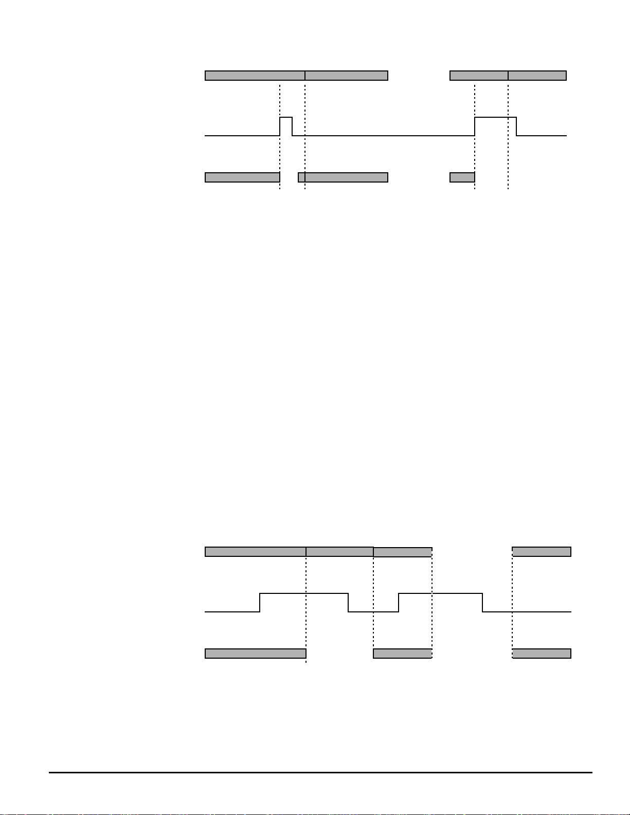
5.4. Cell Marking (CI, NI, PTI)
Figure 10 illustrates two MC92501 devices connected to a
switch fabric. In this example, the ABR ßow travels from left to
right. This means that data cells are ßowing from left to right,
FRM cells are ßowing from left to right, and BRM cells are
ßowing from right to left. The switch marks FRM and user cells
Ingress Flow Status
Ingress User Cell Marking (EFCI)
Ingress FRM Cell Marking (CI or NI)
Egress BRM Cell Marking (CI or NI)
EFCI, FRM
BRM
Ingress
Switch Fabric
Egress
MC92501 #1 MC92501 #2
ßowing downstream, and BRM cells ßowing upstream. This
switch function can be implemented in the ingress of MC92501
#1 and in the egress of MC92501 #2. MC92501 #1 marks cells
because of the ingress ßow status (for example, ingress ßow
congestion) while MC92501 #2 marks cells because of the
egress ßow status.
Egress Flow Status
Egress User Cell Marking (EFCI)
Egress FRM Cell Marking (CI or NI)
Ingress BRM Cell Marking (CI or NI)
Egress
Ingress
Downstream Direction
Upstream Direction
Figure 10. ABR Flow Cell Marking Example
The MC92501 can take the following actions in response to
the ingress ßow status:
¥ Perform EFCI marking on ingress cells; i.e., set PTI[1] bit
in cells on which PTI[2] = 0.
¥ Set CI or NI in ingress FRM cells.
¥ Set CI or NI in egress BRM cells.
The MC92501 can take the following actions in response to
the egress ßow status:
¥ Perform EFCI marking on egress cells; i.e., set PTI[1] bit
in cells on which PTI[2] = 0.
¥ Set CI or NI in egress FRM cells.
¥ Set CI or NI in ingress BRM cells.
Figure 11 is an overview of the MC92501 marking scheme.
MOTOROLA
MC92501
13
Page 14
OR
Global Reg.
CellÕs Overhead
Context Bit
Ingress
Status
Collection
Global Registers
Ingress Flow Status
Ingress
Action:
Marking
Global Registers
Context Bits
Cell Type
Set CI
Set NI
Set PTI
Global Reg.
CellÕs Overhead
Context Bit
Egress
Status
Collection
Egress Flow Status
Figure 11. Cell Marking Scheme
There are various ways to inform the MC92501 that it should
mark a cell due to the ingress ßow status or the egress ßow
status. This scheme also shows that the status of the ingress
ßow, the status of the egress ßow, global registers, a context
bit, and the cell type impact the decision of setting CI, NI, and
PTI. Following is a detailed description of each of the function
boxes.
5.4.1. Sources for Ingress Flow Status
The ingress ßow status is gathered from three sources:
global register, cellÕs overhead, or context bit.
5.4.1.1. Ingress Flow Status from Global Register
The switch fabric can notify the MC92501 that it should mark
cells because of the ingress ßow status by setting the
Global Ingress ABR Mark Enable
bit in the Ingress Processing
Control Register (IPLR).
5.4.1.2. Ingress Flow Status from CellÕs Overhead
The switch fabric can notify the MC92501 that it should mark
cells because of the ingress ßow status of connection #n by
setting the
IFSÑOverhead Ingress Flow Status bit in the
overhead of egress cells belonging to that connection. The
location of this bit in the overhead is programmable using the
EIBYÑIFS Byte Location bit and the EIBIÑIFS Bit Location
bit in the Egress Switch Overhead Information Register 1
(ESOIR1). This bit is enabled by the
EIASÑGlobal IFS Enable
bit in the Egress Switch Interface ConÞguration Register
(ESWCR). The MC92501 can be programmed that in such a
case it will mark egress BRM cells.
IAMEÑ
Set CI
Egress
Action:
Marking
Section 5.4.1.2 for details on enabling of
Ingress Flow Status
receives that cell, it copies the bit into the
Ingress Flow Status
Set NI
Set PTI
IFSÑOverhead
bit and its location.) When the MC92501
CIFSÑConnection
bit in the Common Parameters Extension
Word of connection #n. The MC92501 can be programmed
that in such a case it will mark ingress FRM cells or perform
EFCI marking.
5.4.1.4. Logic of Ingress Flow Status
The ingress ßow status equals 1 if:
IAME = 1
IFS = 1 and EIAS = 1 and egress = 1 OR
CIFS = 1 and EIAS = 1 and ingress = 1
Where:
IAME = Global Ingress ABR Mark Enable
IFS = Overhead Ingress Flow Status
EIAS = Global IFS Enable
CIFS = Connection IFS Enable
Egress = Programmed Overhead Egress Bit
Ingress = Programmed Overhead Ingress Bit
5.4.2. Sources for Egress Flow Status
The egress ßow status is gathered from three sources:
global register, cellÕs overhead, and context memory.
5.4.2.1. Egress Flow Status from Global Register
The switch fabric can notify the MC92501 that it should mark
cells because of the egress ßow status by setting the
Global Egress ABR Mark Enable
bit in the Egress Processing
EAMEÑ
Control Register (EPLR).
5.4.1.3. Ingress Flow Status from Context Memory
The switch fabric can notify the MC92501 that it should mark
cells because of the ingress ßow status of connection #n by
setting the
IFSÑOverhead Ingress Flow Status bit in the
overhead of egress cells belonging to that connection. (See
MC92501
14
5.4.2.2. Egress Flow Status from CellÕs Overhead
The switch fabric can notify the MC92501 that it should mark
cells because of the egress ßow status of connection #n by
setting the
EFSÑOverhead Egress Flow Status bit in the
overhead of egress cells belonging to that connection. The
MOTOROLA
Page 15

location of this bit in the overhead is programmable using the
EEBYÑEFS Byte Location bit and the EEBIÑEFS Bit
Location
Register 1 (ESOIR1). This bit is enabled by the
EFS Enable
Register (ESWCR). The MC92501 can be programmed that
in such a case it will mark egress FRM cells or perform EFCI
marking.
5.4.2.3. Egress Flow Status from Context Memory
cells because of the egress ßow status of connection #n by
setting the
overhead of egress cells belonging to that connection. (See
Section 5.4.2.2 for details on enabling of EFSÑOverhead
Egress Flow Status bit and its location.) When the MC92501
receives that cell, it copies the bit into the CEFSÑConnection
Egress Flow Status bit in the Common Parameters Extension
Word of connection #n. The MC92501 can be programmed
that in such a case it will mark ingress BRM cells.
5.4.2.4. Logic of Egress Flow Status
5.4.3. Ingress ABR Marking Bits
ßow status or egress ßow status.
MC92501 can perform one or more of the following:
¥ Set CI bit in an ingress FRM cell Ñ when the ISFCEÑ
¥ Set NI bit in an ingress FRM cell Ñ when the ISFNEÑ
¥ Set PTI[1] bit in an ingress cell whose PTI[2] = 0 Ñ when
MC92501 can perform one or more the following:
¥ Set CI bit in an ingress BRM cell Ñ when the ISBCEÑ
¥ Set NI bit in an ingress BRM cell Ñ when the ISBNEÑ
bit in the Egress Switch Overhead Information
EEASÑGlobal
bit in the Egress Switch Interface ConÞguration
The switch fabric can notify the MC92501 that it should mark
EFSÑOverhead Egress Flow Status bit in the
The egress ßow status equals 1 if:
EAME = 1 OR
EFS = 1 and EEAS = 1 and egress = 1 OR
CEFS = 1 and EEAS = 1 and ingress = 1
Where:
EAME = Global Egress ABR Mark Enable
EFS = Overhead Egress Flow Status
EEAS = Global EFS Enable
CEFS = Connection EFS Enable
Egress = Programmed Overhead Egress Bit
Ingress = Programmed Overhead Ingress Bit
The MC92501 can mark cells as a result of either ingress
In the case where ingress ßow status is asserted, the
Global Ingress Set FRM CI Enable bit in the Ingress
Processing ConÞguration Register (IPCR) is set.
Global Ingress Set FRM NI Enable bit in the IPCR is set.
the ISPEÑGlobal Ingress Set PTI Enable bit in the IPCR
is set.
In the case where egress ßow status is asserted, the
Global Ingress Set BRM CI Enable bit in the IPCR is set.
Global Ingress Set BRM NI Enable bit in the IPCR is set.
All cell marking on the ingress is enabled on a per-
connection basis by the CIMEÑConnection Ingress Marking
Enable bit in the Common Parameters Extension Word.
5.4.3.1. Logic of Ingress ABR Marking Bits
The CI bit is set if:
FRM cell and CIME = 1 and ingress ßow status = 1
and ISFCE = 1 OR
BRM cell and CIME = 1 and egress ßow status = 1
and ISBCE = 1
The NI bit is set if:
FRM cell and CIME = 1 and ingress ßow status = 1 and
ISFNE = 1 OR
BRM cell and CIME = = 1 and egress ßow status = 1 and
ISBNE = 1
The PTI[1] bit is set if:
PTI[2] = 0 and CIME = 1 and ingress ßow status = 1 and
ISPE = 1
Where:
CIME = Connections Ingress Marking Enable
FRM Cell = Cell marked as FRM cell
BRM Cell = Cell marked as BRM cell
Ingress Flow Status = Set as deÞned in Section 5.4.1.4
Egress Flow Status = Set as deÞned in Section 5.4.2.4
ISFCE = Global Ingress Set FRM CI Enable
ISFNE = Global Ingress Set FRM NI Enable
ISPE = Global Ingress Set PTI Enable
ISBCE = Global Ingress Set BRM CI Enable
ISBNE = Global Ingress Set BRM NI Enable
5.4.4. Egress ABR Marking Bits
The MC92501 can mark cells as a result of either ingress
ßow status or egress ßow status.
In the case where egress ßow status is asserted, the
MC92501 can perform one or more of the following:
¥ Set CI bit in an egress FRM cell Ñ when the ESFCEÑ
Global Egress Set FRM CI Enable bit in the Egress
Processing ConÞguration Register (EPCR) is set.
¥ Set NI bit in an egress FRM cell Ñ when the ESFNEÑ
Global Egress Set FRM NI Enable bit in the EPCR is set.
¥ Set PTI[1] bit in an egress cell whose PTI[2] = 0 Ñ when
the ESPEÑGlobal Egress Set PTI Enable bit in the EPCR
is set.
In the case where ingress ßow status is asserted, the
MC92501 can perform one or more the following:
¥ Set CI bit in an egress BRM cell Ñ when the ESBCEÑ
Global Egress Set BRM CI Enable bit in the EPCR is set.
¥ Set NI bit in an egress BRM cell Ñ when the ESBNEÑ
Global Egress Set BRM NI Enable bit in the EPCR is set.
All cell marking on the egress is enabled on a per-
connection basis by the CEMEÑConnection Egress Marking
Enable bit in the Common Parameters Extension Word.
MOTOROLA
MC92501
15
Page 16
5.4.4.1. Logic of Egress ABR Marking Bits
The CI bit is set if:
FRM cell and CEME = 1 and egress ßow status = 1
and ESFCE = 1 OR
BRM cell and CEME = 1 and ingress ßow status = 1
and ESBCE = 1
The NI bit is set if:
FRM cell and CEME = 1 and egress ßow status = 1 and
ESFNE = 1 OR
BRM cell and CEME = 1 and ingress ßow status = 1 and
ESBNE = 1
The PTI[1] bit is set if:
PTI[2] = 0 and CEME = 1 and egress ßow status = 1 and
ESPE = 1
Where:
CEME = Connections Egress Marking Enable
FRM Cell = Cell marked as FRM cell
BRM Cell = Cell marked as BRM cell
Ingress Flow Status = Set as deÞned in Section 5.4.1.4
Egress Flow Status = Set as deÞned in Section 5.4.2.4
ESFCE = Global Egress Set FRM CI Enable
ESFNE = Global Egress Set FRM NI Enable
ESPE = Global Egress Set PTI Enable
ESBCE = Global Egress Set BRM CI Enable
ESBNE = Global Egress Set BRM NI Enable
5.4.5. Cell Marking Examples
Figure 12, Figure 13, and Figure 14 provide examples for
CI and NI marking.
NOTE 1
NOTE 3
NOTE 4
MC92501 #1 MC92501 #2
NOTES:
1. Initially the microprocessor conÞgures the MC92501 #1 as follows:
¥ Sets the ISFCEÑGlobal Ingress Set FRM CI Enable bit.
¥ Sets the CIMEÑConnection Ingress Marking Enable bit for selected ABR connections.
2. The switch fabric informs the microprocessor that ingress ABR queues have reached
some limit.
3. The microprocessor sets the IAMEÑGlobal Ingress ABR Mark Enable bit.
4. The MC92501 sets the CI bit for FRM cells belonging to the selected ABR connections.
Microprocessor
NOTE 2
Switch Fabric
Downstream Direction
Upstream Direction
Figure 12. Enable Marking CI Bits of Ingress FRM Cells
MC92501
16
MOTOROLA
Page 17

NOTE 1
Microprocessor
NOTE 3
MC92501 #1 MC92501 #2
NOTES:
1. Initially the microprocessor conÞgures the MC92501 #1 as follows:
¥ Sets the EIASÑGlobal IFS Enable bit.
¥ Sets the ESBNEÑGlobal Egress Set BRM NI Enable bit.
¥ Programs the location of the IFSÑOverhead Ingress Flow Status bit by writing to the EIBYÑIFS Byte Location and the EIBIÑIFS
Bit Location Þelds.
On connection setup the microprocessor conÞgures the MC92501 #1 as follows:
¥ Sets the CEMEÑConnection Egress Marking Enable bit for selected ABR connections.
2. The switch detects that the ingress queue of connection #n has reached a limit. It sets ingress ßow status bit on the overhead of
cells belonging to that connection.
3. The MC92501 sets the NI bit of BRM cell belonging to connection #n.
NOTE 2
Switch Fabric
Downstream Direction
Upstream Direction
Figure 13. Egress Flow Contains Ingress Flow Status and Causes the MC92501 to Mark BRM Cell NI Field
Microprocessor
NOTE 1
NOTE 2
NOTE 3
Switch Fabric
MC92501 #1 MC92501 #2
Downstream Direction
Upstream Direction
NOTES:
1. Initially the microprocessor conÞgures the MC92501 #2 as follows:
¥ Sets the EEASÑGlobal EFS Enable bit.
¥ Sets the ISBCEÑGlobal Ingress Set BRM CI Enable bit.
¥ Programs the location of the EFSÑOverhead Egress Flow Status bit by writing to the EEBYÑEFS Byte Location and the EEBIÑ
EFS Bit Location Þelds.
On connection setup the microprocessor conÞgures the MC92501 #2 as follows:
¥ Sets the CEMEÑConnection Egress Marking Enable bit for selected ABR connections.
2. The switch detects that the egress queue of connection #n has reached a limit. It sets egress ßow status bit on the overhead of cells
belonging to that connection.
3. The MC92501 copies the overhead egress ßow status bit into the CEFSÑConnection Egress Flow Status bit and effectively sets it.
4. The MC92501 sets the CI bit of BRM cells belonging to connection #n.
NOTE 4
Figure 14. Egress Flow Contains Egress Flow Status for Connection #n Causes the MC92501 to Mark CI Bit
of All Ingress BRM Cells Belonging to That Connection
MOTOROLA
MC92501
17
Page 18

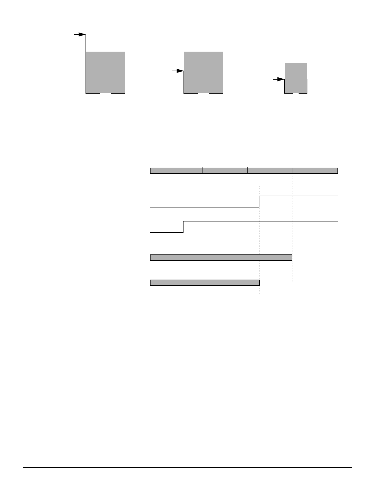
5.5. Ingress Switch ABR Priority Interface
The MC92501 deÞnes an 8-bit Þeld which can be overlayed
on bits of the ingress switch parameters belonging to RM cells.
In applications where the overlayed switch parameter Þeld is
a priority Þeld which is used by the switch fabric, RM cells can
gain higher priority in passing the switch and thus enable
shortening the feedback loop for ABR.
The MC92501 performs this Þeld overlay if one of the
following occurs:
¥ An ingress BRM cell is received and both the IBOEÑ
Ingress BRM Overlay Enable bit and the IROEÑIngress
RM Overlay Enable bit are set.
WRITE HERE IF CELL IS A BRM
Byte #8 Byte #9 Byte #10 Byte #11
1
Switch Params #2
Byte #4 Byte #5 Byte #6 Byte #7
Switch Params #1
Byte #0 Byte #1 Byte #2 Byte #3
Switch Params #0
001
¥ An ingress FRM cell is received and both the IFOEÑ
Ingress FRM Overlay Enable bit and the the IROEÑ
Ingress RM Overlay Enable bit are set.
Once the MC92501 is enabled, it uses the ROLÑRM
Overlay Location Þeld in order to locate one byte out of 12
bytes on the ingress switch parameters. This byte is overlaid
by the ROFÑRM Overlay Þeld only on bits which are enabled
by the ROMÑRM Overlay Mask Þeld.
See Section 11.4.12 for Þeld descriptions.
5.5.1. An Example
Figure 15 demonstrates the ingress switch APB priority
interface, supposing that the ROF Þeld = 11001101, the ROM
Þeld = 01111000, the ROL Þeld = 9, the IBOE bit is set, and
that the current cell is a backward RM cell.
Figure 15. Example of Ingress Switch ABR Priority Interface
5.6. Egress Reset EFCI
The MC92501 resets PTI[1] on a cell which meet the
following conditions:
¥ Its PTI[2] = 0.
¥ It is a non-RM cell.
¥ The EREFÑEgress Reset EFCI bit in the Context
Parameters Extension Table for the connection to which
the cell belongs is set.
¥ This feature can be used as part of Òdestination behavior.Ó
Egress Reset EFCI is enabled globally by the EPCVÑ
Egress Features Enable bit in the ACR.
MC92501
18
MOTOROLA
Page 19

SECTION 6. CLP TRANSPARENCY
6.1. Overview
The trafÞc management speciÞcation deÞnes two network
operation models with relation to CLP = 1 ßow: CLP
transparent and CLP signiÞcant. A connection which is CLP
transparent does not have different Cell Loss Ratio (CLR) for
CLP = 0 or CLP = 1 trafÞc, and therefore does not prefer
discarding CLP = 1 over CLP = 0 cells on congestion. Current
switch fabrics do distinguish globally between CLP = 0 trafÞc
and CLP = 1 trafÞc with the CLP = 1 trafÞc being more
susceptible to discarding in case of congestion.
The MC92501 solves the problem in the following manner:
¥ If a cell belongs to a connection which supports CLP
transparency (the ICTEÑIngress CLP Transparency
Enable bit in the Common Parameters Extension Word is
set), then the MC92501 moves the CLP from the cellÕs
ICTVÑIngress CLP Transparency Value
NOTE 1
PayloadOverhead Header
header to IOCLPÑIngress Overhead CLP bit in the cellÕs
overhead and assigns 0 to the header CLP.
¥ The cell is forwarded to the switch fabric. The switch fabric
considers the cell as if it has CLP = 0.
¥ On the egress side, the MC92501 reconstructs the header
CLP from the EOCLPÑEgress Overhead CLP bit in the
cellÕs overhead.
In order to support other applications, the MC92501 function
is extended as follows. It assigns the ICTVÑIngress CLP
Transparency Value bit (deÞned in the Common Parameters
Extension Word) to the cellÕs header instead of 0. If the ICTVÑ
Ingress CLP Transparency Value bit = 0 then we are back at
the CLP transparency application. CLP Transparency is
enabled globally by the IPCVÑIngress Features Enable bit in
the ACR register.
NOTE 2
Overhead
Header
Payload
Switch Fabric
MC92501 #1 MC92501 #2
NOTES:
1. If a cell belongs to a connection which supports CLP transparency (the ICTEÑIngress CLP Transparency Enable bit
is set), then MC92501 moves the CLP from the cellÕs header to the IOCLPÑIngress Overhead CLP bit in the cellÕs
overhead and assigns the ICTVÑIngress CLP Transparency Value bit to the header CLP.
2. If the CIFSÑConnection Ingress Flow Status bit is set then the MC92501 reconstructs the header CLP from the
EOCLPÑEgress Overhead CLP bit in the cellÕs overhead.
Figure 16. CLP Transparency with a CLP Significant Switch Fabric
The IOCLPÑIngress Overhead CLP bit location is
programmable using the OCBLÑIOCLP Bit Location Þeld in
the Ingress Switch Interface ConÞguration Register (ISWCR).
The EOCLPÑEgress Overhead bit location is
programmable using the EOBYÑEOCLP Byte Location Þeld
and the EOBIÑEOCLP Bit Location Þeld in the Egress Switch
Overhead Information Register 1 (ESOIR1).
MOTOROLA
MC92501
19
Page 20

SECTION 7. INDIRECT EXTERNAL MEMORY ACCESS
7.1. Overview
The MC92500 allows the processor to access its external
memory for the duration of one cell processing time out of N,
where N is programmable. The MC92501 will additionally
allow the processor to access external memory while
operating on the cell stream. The indirect access takes place
at least once in every cell processing slot. The indirect access
is not performed during maintenance.
7.2. User Interface
Indirect external memory access is performed using two
registers: the Indirect External Memory Access Address
Register (IAAR) and the Indirect External Memory Access
Data Register (IADR).
7.2.1. Write Access
In order to write to the external memory, the processor
should poll the IABÑIndirect External Memory Access Busy
bit in the IAAR register to verify the status of the IAAR and
IADR registers. If IAB is clear, then the processor can write
the address data and status into the appropriate registers. The
IADÑIndirect External Memory Address DIR bit is is set to 0
for a write operation. Writing to the IAAR register triggers the
MC92501 to wait for a dedicated clock to write the data into
the external memory using the given address and data. Once
the MC92501 Þnishes writing, it clears the IABÑIndirect
External Memory Access Busy bit in the IAAR register.
7.2.2. Read Access
In order to read from the external memory, the processor
should poll the IABÑIndirect External Memory Access Busy
bit in the IAAR register to verify that it may write the IAAR
register. If IAB is clear, then the processor can write the
address, size, and direction into the appropriate registers. For
a read operation, the IADÑIndirect External Memory Address
DIR bit is set to 1. Writing to the IAAR register triggers the
MC92501 to wait for a dedicated clock, and read the data from
external memory using the given address and write the data
into the IADR register. Once the data was written into the IADR
register, the MC92501 clears the IABÑIndirect External
Memory Access Busy bit in the IAAR register. The processor
then may read the data from the IADR register.
The address space which is covered by this interface
includes all the non-destructive external memory access and
an external address compression device.
NOTE
Indirect write access to an external memory
space, which can be written by the MC92501, is
not recommended. For example, an indirect write
access to a ßag-table record of an active
connection is not recommended. It is advisable to
use the maintenance cell slot for this purpose.
Table 1 summarizes indirect access Þelds:
Table 1. Indirect Access Fields
IADÑ
Indirect
External
Memory
Access DIR
0 0 x x Write IADR[31:00] to external memory word bits [31:00]
0 1 0 0 Write IADR[31:16] to external memory word [31:16]
0 1 0 1 Write IADR[15:00] to external memory word [15:00]
0 1 1 0 Write IADR[15:00] to external memory word [15:00]
0 1 1 1 Write IADR[31:16] to external memory word [31:16]
1 x x x Read external memory word bits [31:00] to IADR[31:00]
IAWÑ
Indirect
External
Memory
Access Size
Least
SigniÞcant
Bit of IAAÑ
Indirect
External
Memory
Access
Address
DOÑData
Order
Function
MC92501
20
MOTOROLA
Page 21

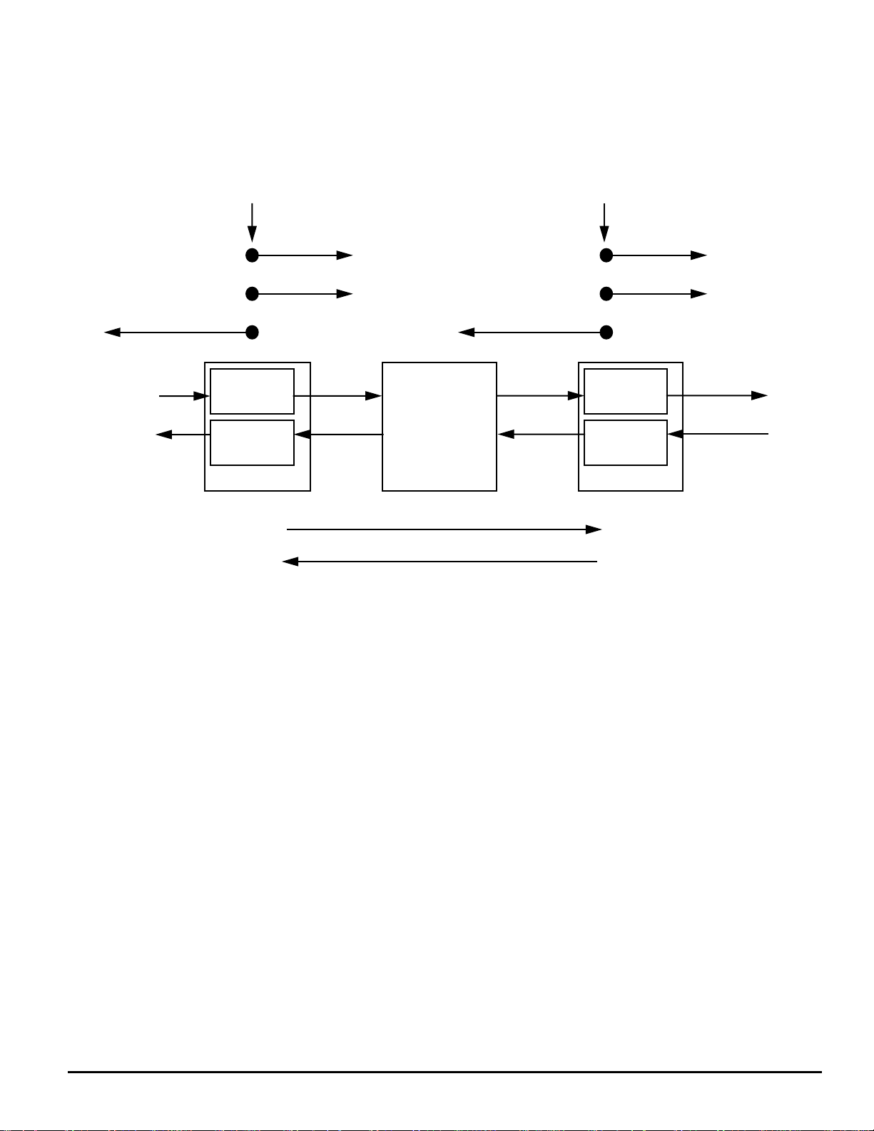
SECTION 8. IMPROVED HOST INTERFACE
8.1. Overview
In order to improve the MC92501 interface to the
microprocessor, the following features were added:
8.1.1. An Additional MDTACK
The MDT
on which there are two MDT
ACK signals enable a glueless interface to systems
ACK signals and their combination
conveys the bus width of the slave. The MDT
driven only when the MDT
ACK0 signal is driven and when the
MDCÑMDTACK Drive Control is set.
8.1.2. Programmable MREQ
The MC92500 generates three DREQ
for external memory request, MCIREQ for cell insertion
request, and MCOREQ
for cell extraction request. The
MC92501 changes the functionality (and the name) of the
three DREQ
lines. Each MREQ[n] line may be connected to
each of the internal requests: external memory, cell insertion,
or cell extraction. If a system contains three DMAs, then each
DMA may be connected to a different DMA DREQ
WSSMÑWord Select Signals
Mode = 0
Signal
ACK1 signal is
Signals
signals: EMMREQ
signal. In
Table 2. Host Interface Fields
WSSMÑWord Select Signals
Mode = 1
and
DOÑData Order = 0
systems with less than three DMAs, each such DMA should
switch between the MREQ
lines. This switching can be done
when using the MC92500 through the use of glue logic. In
these cases, this feature enables a glueless interface. The
MREQ
signals default to the MC92500 conÞguration so that
backwards compatibility is maintained.
8.1.3. Update the Definition of MWSH
and MWSL
Signals
MWSH
and MWSL are used in MC92500 as word select
during external memory accesses. Some systems assert
these signals only during write cycles. The MC92501 uses
these signals only on external memory write accesses. Read
accesses are always performed regardless of these signals.
Moreover, another use of these signals is for systems to use
them for Address[1] bit and SIZE. The MC92501 supports
another deÞnition for the same pins: MWSH
Address[1] while MWSL
can serve as SIZE. The WSSMÑ
pin can serve as
Word Select Signals Mode bit selects which mode is
supported. Table 2 describes the pinsÕ functionality:
WSSMÑWord Select Signals
Mode = 1
and
DOÑData Order = 1
Function
MWSH MWSL A1 Size A1 Size
0 0 x 0 x 0 Write D(31:0)
0 1 0 1 1 1 Write D(31:16)
1 0 1 1 0 1 Write D(15:00)
MOTOROLA
MC92501
21
Page 22

SECTION 9. EGRESS OVERHEAD MANIPULATION
The MC92501 supports the following features:
¥ The size of the ECI Þeld used by the egress cell processing
block can be programmed by writing to the ECESÑEgress
Cell Processing Block ECI Size Þeld in the Egress
Overhead Manipulation Register (EGOMR).
¥ The size of the MTTS Þeld used by the egress cell
processing block can be programmed by writing to the
ECTSÑEgress Cell Processing Block MTTS Size Þeld in
the EGOMR.
¥ The M bit used by the egress cell processing block can be
either the M bit which was extracted from the cellÕs
overhead, the logical not of the M bit which was extracted
from the cellÕs overhead, or 1 or 0 by programming the
ECMSÑEgress Cell Processing Block M Bit Source Þeld
in the EGOMR.
¥ In ECI on Header mode, the ECI is extracted from the ATM
cell header. The header VPI Þeld size can be programmed
to either 12 bits or 8 bits using the VPSÑVPI Size in ECI
on Header Mode bit of the Egress Switch Interface
ConÞguration Register (ESWCR).
MC92501
22
MOTOROLA
Page 23

SECTION 10. UTOPIA LEVEL 2 PHY INTERFACE
The MC92501 PHY interface can be programmed to
support UTOPIA Level 2. It allows for operation of one TxClav
and one RxClav signal.
On the ingress direction, the MC92501 supports address
polling on up to 16 physical links. It scans all the links in a
round robin fashion and decides from which PHY to read the
next cell.
UTOPIA Level 2 is enabled on ingress by programming the
IUMÑIngress UTOPIA Mode bit of the Ingress PHY
ConÞguration Register (IPHCR). In this mode, Receive PHY
ID 0-3/Receive Address 0-3 (RXPHYID0-RXPHYID3/
RXADD0-RXADDR3) signals function as RXADDR0-
RXADDR4.
NOTE
RXADDR4 is a new functional signal in MC92501
that was a NC (No Connect) on the MC92500.
PHY Device
PHY Device
TxAddr
UTOPIA Level 2 is enabled on egress by programming the
EUMÑEgress UTOPIA Mode bit of the Egress PHY
ConÞguration Register (EPHCR). In this mode, the Transmit
PHY ID 0-3 /Transmit Address 0-3 (TXPHYID0-TXPHYID3/
TXADDR0-TXADDR3) signals and the Transmit Next PHY ID
Valid/Transmit Address 4 (TXPHYIDV/TXADDR4) signal are
used as TXADDR0-TXADDR4. The MC92501 polls the link of
the cell in its egress PHY IF FIFO, and when enabled it outputs
the cell to the link PHY. The MC92501 performs address
polling on all other links as well in order to enable external
logic to monitor the PHYÕs status.
Figure 17 illustrates an application on which external logic
monitors the RxClav signal while the MC92501 is polling the
PHY devices. Based on this information, the external logic can
input cells to the MC92501 egress ßow.
MC92501
PHY Device
PHY Device
Feedback
TxAddr
TxClav
External Logic
Figure 17. Feedback Using TxClav
MOTOROLA
MC92501
23
Page 24

SECTION 11. REGISTER DESCRIPTIONS
This section describes the registers which were added or modiÞed for the MC92501.
11.1. General Register List
Table 3 contains all the registers which were added and their addresses.
Table 3. General Register List
Register Group Register Name Mnemonic ADD (25:0) Ref.
Page
Control
Registers
ConÞguration
Register
Ingress Processing Control Register IPLR 0030824 25
Egress Processing Control Register EPLR 0030828 25
Indirect External Memory Access Address Register IAAR 0030810 26
Indirect External Memory Access Data Register IADR 0030814 26
Egress Switch Overhead Information Register 1 ESOIR1 0030818 32
RM Overlay Register RMOR 003081C 33
Egress Overhead Manipulation Register EGOMR 0030820 34
Common Parameters Extension Table Pointer Register CPETP 0030d88 33
CLP Transparency Overlay Register CTOR 003082C 33
11.2. Status Reporting Registers
The following registers have been updated. The Þelds that have been added are in bold.
11.2.1. Interrupt Register (IR)
The FQF bit has been added.
31 30 29 28 27 26 25 24 23 22 21 20 19 18 17 16
OMCMMSE0000SPD00FQF CIQE CEQR CEQI CEQL CEQF
1514131211109876543210
0 0 UDI50 UDI40 UDI30 UDI20 UDI1ESPEUDI0ESHE0 0 0 IPPE IPHE FQO FQEO MNAE
FQFÑFMC Queue Full
This bit reports that the internal FMC queue is full. The reason for this is that the FMC generation rate is higher then the allocated
insertion bandwidth. Insertion rate is controlled by the insertion leaky bucket.
11.2.2. Interrupt Mask Register (IMR)
The FQFE bit has been added.
31 30 29 28 27 26 25 24 23 22 21 20 19 18 17 16
OME CME MSEE 0000SPDE 0 0 FQFE CIQEE CEQRE CEQIE CEQLE CEQFE
1514131211109876543210
0 0 UDIE50 UDIE40 UDIE30 UDIE20 UDIE1E
SPEE
UDIE0E
SHEE
0 0 0 IPPEE IPHEE FQOE FQEOE MNAEE
FQFEÑFMC Queue Full Interrupt Enable
When FQF and FQFE are set, an interrupt is generated.
MC92501
24
MOTOROLA
Page 25

11.2.3. ATMC CFB Revision Register (ARR)
The AMRV Þeld has been updated.
Table 4. Values of ATMC CFB Revision Fields
AMRV ASRV ATMC CFB Revision
000001 000000 MC92501 (MC92500 Revision B)
11.2.4. MC92501 Revision Register (RR)
The MRV Þeld has been updated.
Table 5. Values of the MC92501 Revision Fields
ID MRV SRV MC92501 Revision
10000000000000000000 000001 000000 MC92501 (MC92500 Revision B)
11.3. Control Registers
The following registers have been added.
11.3.1. Ingress Processing Control Register (IPLR)
This register has the following structure:
31 30 29 28 27 26 25 24 23 22 21 20 19 18 17 16
0000000000000000
1514131211109876543210
00000000000000ICNG IAME
ICNGÑGlobal Ingress Congestion NotiÞcation
This bit notiÞes the MC92501 whether there is congestion in the ingress ßow. See Section 4.
0 = No ingress congestion.
1 = Ingress congestion. The MC92501 performs selective discard according to per-connection CIMEÑConnection Ingress
Marking Enable bit.
IAMEÑGlobal Ingress ABR Mark Enable
This bit, when set, indicates that current ingress ßow status implies that the MC92501 should perform RR marking and/or EFCI
marking if enabled. See Section 5.4.1.
11.3.2. Egress Processing Control Register (EPLR)
This register has the following structure:
31 30 29 28 27 26 25 24 23 22 21 20 19 18 17 16
0000000000000000
1514131211109876543210
000000000000000EAME
EAMEÑGlobal Egress ABR Mark Enable
This bit, when set, indicates that current egress ßow status implies that the MC92501 should perform RR marking and/or EFCI
marking if enabled. See Section 5.4.2.
MOTOROLA
MC92501
25
Page 26

11.3.3. Indirect External Memory Access Address Register (IAAR)
This register contains the address, width, and busy bit for accessing the MC92501 external memory or the external memory
device. Refer to Section 7 for details. The register has the following structure:
31 30 29 28 27 26 25 24 23 22 21 20 19 18 17 16
IAB IAD IAW 0 0 0 IAAS IAA
1514131211109876543210
IAA 0
IABÑIndirect External Memory Access Busy
This bit indicates that indirect external memory access mechanism is busy.
0 = Indirect access mechanism is free and therefore indirect external memory access data register can be accessed.
1 = Indirect access mechanism is busy and therefore indirect access data register should not be accessed.
IADÑIndirect External Memory Access DIR
This bit indicates indirect access direction.
0 = Indirect write access
1 = Indirect read access
IAWÑIndirect External Memory Access Size
This bit indicates the size of the access.
0 = 32 bits
1 = 16 bits
IAASÑIndirect External Memory Access Address Space
This Þeld indicates the accessed address space.
00 = Reserved
01 = External address compression device
10 = Non-destructive external memory
11 = Reserved
IAAÑIndirect External Memory Access Address
This Þeld indicates bits 23:1 of the address within the address space speciÞed in the IAASÑIndirect External Memory Access
Address Space Þeld.
11.3.4. Indirect External Memory Access Data Register (IADR)
This register contains the data which should be written to the external memory in case of an indirect write access or the data
that was last read from external memory in case of an indirect read access. Refer to Section 7 for details.
MC92501
26
MOTOROLA
Page 27

11.4. Configuration Register
The following registers have been updated. The Þelds that have been added are in bold.
11.4.1. Ingress Processing Configuration Register (IPCR)
31 30 29 28 27 26 25 24 23 22 21 20 19 18 17 16
00000000IGCTE ICCR IRCR ISFCE ISFNE ISPE ISBCE ISBNE
1514131211109876543210
IPCC 0 IGZC IUHC IIP IROE 0 IBCC IPCV IAPE IACE
IGCTEÑGlobal Ingress CLP Transparency Enable
This bit enables CLP transparency function on the ingress. See Section 6 for details.
ICCRÑIngress Check CRC on RM Cells
This bit determines whether the CRC of RM cells that are received in the ingress is checked.
0 = The CRC of RM cells that are recevied in the ingress is not checked.
1 = The CRC of RM cells that are received in the ingress is checked and if it is not okay, then the cell is removed and can be
copied to the microprocessor.
IRCRÑIngress Recalculate CRC on RM Cells
This bit determines whether the CRC of ingress RM cells is recalculated.
0 = The CRC of ingress RM cells is not recalculated.
1 = The CRC of ingress RM cells is recalculated.
ISFCEÑGlobal Ingress Set FRM CI Enable
This bit enables setting CI bit in forward RM cells received in ingress. See Section 5.4.3 for details.
0 = Setting CI bit in forward RM cells received in ingress is disabled.
1 = Setting CI bit in forward RM cells received in ingress is enabled.
ISFNEÑGlobal Ingress Set FRM NI Enable
This bit enables setting NI bit in forward RM cells received in ingress. See Section 5.4.3 for details.
0 = Setting NI bit in forward RM cells received in ingress is disabled.
1 = Setting NI bit in forward RM cells received in ingress is enabled.
ISPEÑGlobal Ingress Set PTI Enable
This bit enables setting PTI[1] bit in cells with PTI[2] = 0 which are received in ingress. See Section 5.4.3 for details.
0 = Setting PTI[1] bit in cells with PTI[2] = 0 which are received in ingress is disabled.
1 = Setting PTI[1] bit in cells with PTI[2] = 0 which are received in ingress is enabled.
ISBCEÑGlobal Ingress Set BRM CI Enable
This bit enables setting CI bit in backward RM cells received in ingress. See Section 5.4.3 for details.
0 = Setting CI bit in backward RM cells received in ingress is disabled.
1 = Setting CI bit in backward RM cells received in ingress is enabled.
ISBNEÑGlobal Ingress Set BRM NI Enable
This bit enables setting NI bit in backward RM cells received in ingress. See Section 5.4.3 for details.
0 = Setting NI bit in backward RM cells received in ingress is disabled.
1 = Setting NI bit in backward RM cells received in ingress is enabled.
IROEÑIngress RM Overlay Enable
This bit enables updating switch parameter words in the case of RM cells. See Section 5.5 for details.
IPCVÑIngress Features Enable
This bit should be set when the following features are used: packet-based UPC, selective discard, and CLP transparency.
MOTOROLA
MC92501
27
Page 28

11.4.2. Egress Processing Configuration Register (EPCR)
31 30 29 28 27 26 25 24 23 22 21 20 19 18 17 16
00000000EGCTE ECCR ERCR ESFCE ESFNE ESPE ESBCE ESBNE
1514131211109876543210
EPCC 000EIP 0 0 EBCC EPCV RGFC 0 0
EGCTEÑGlobal Egress CLP Transparency Enable
This bit enables CLP transparency function on the egress. See Section 6 for details.
ECCRÑEgress Check CRC on RM Cells
This bit determines whether the CRC of RM cells that are received in the egress is checked.
0 = The CRC of RM cells that are recevied in the egress is not checked.
1 = The CRC of RM cells that are received in the egress is checked and if it is not okay, then the cell is removed and can be
copied to the microprocessor.
ERCRÑEgress Recalculate CRC on RM Cells
This bit determines whether the CRC of egress RM cells is recalculated.
0 = The CRC of egress RM cells is not recalculated.
1 = The CRC of egress RM cells is recalculated.
ESFCEÑGlobal Egress Set FRM CI Enable
This bit enables setting CI bit in forward RM cells received in egress. See Section 5.4.2.
0 = Setting CI bit in forward RM cells received in egress is disabled.
1 = Setting CI bit in forward RM cells received in egress is enabled.
ESFNEÑGlobal Egress Set FRM NI Enable
This bit enables setting NI bit in forward RM cells received in egress. See Section 5.4.2.
0 = Setting NI bit in forward RM cells received in egress is disabled.
1 = Setting NI bit in forward RM cells received in egress is enabled.
ESPEÑGlobal Egress Set PTI Enable
This bit enables setting PTI[1] bit in cells with PTI[2] = 0 which are received in egress. See Section 5.4.2.
0 = Setting PTI[1] bit in cells with PTI[2] = 0 which are received in egress is disabled.
1 = Setting PTI[1] bit in cells with PTI[2] = 0 which are received in egress is enabled.
ESBCEÑGlobal Egress Set BRM CI Enable
This bit enables setting CI bit in backward RM cells received in egress. See Section 5.4.2.
0 = Setting CI bit in backward RM cells received in egress is disabled.
1 = Setting CI bit in backward RM cells received in egress is enabled.
ESBNEÑGlobal Egress Set BRM NI Enable
This bit enables setting NI bit in backward RM cells received in egress. See Section 5.4.2.
0 = Setting NI bit in backward RM cells received in egress is disabled.
1 = Setting NI bit in backward RM cells received in egress is enabled.
EPCCÑEgress Policing Counters Control
This Þeld determines which counters appear in the Policing Counters Table if egress UPC is enabled. (The UPCFÑUPC Flow
bit in the ACR is set.) It also determines the size of each record in the table.
000 = The policing table does not exist.
001 = The policing table contains three counters and one reserved long word: DSCD0, DSCD1, TAG, Reserved.
010 = The policing table contains three counters: DSCD0, DSCD1, TAG.
011 = The policing table contains two counters: DSCD, TAG.
100 = The policing table contains one counter: TAG.
101 = The policing table contains one counter: DSCD.
110 = Reserved
111 = Reserved
MC92501
28
MOTOROLA
Page 29

EIPÑEgress Insertion Priority
This bit determines the priority between inserted/generated cells and egress received cells.
Note that insertion is always limited by the leaky bucket mechanism.
0 = Inserted/generated cellsÕ priority is higher than egress received cells.
1 = Egress received cellsÕ priority is higher than inserted/generated cells.
EPCVÑEgress Features Enable
This bit should be set when the reset EFCI feature is activated. See Section 5.6.
11.4.3. ATMC CFB Configuration Register (ACR)
31 30 29 28 27 26 25 24 23 22 21 20 19 18 17 16
ATC SPC COMC INPC EGPC DVTC FLGC OAMC VPRP FTM CRRP PMAC
1514131211109876543210
UPCF 000000000000000
VPRPÑVP RM Cell PTI
This bit determines whether a cell is a VP RM cell only if its PTI = 6.
0 = A cell is a VP RM cell if and only if it belongs to a VP connection, its VCI = 6, and its PTI = 6.
1 = A cell is a VP RM cell if and only if it belongs to a VP connection and its VCI = 6.
CRRPÑVC RM Cell Removal Point
This bit determines whether a VC cell whose PTI = 6 or 7 is removed at the OAM termination point, or whether its removal is
subjected to the per-connection enable bits for PTI = 6 or PTI = 7.
0 = A VC cell whose PTI = 6 or 7 is removed at the OAM termination point as deÞned by the EEOTÑEgress End-to-End
OAM Termination bit in the egress and by the IEOTÑIngress End-to-End OAM Termination bit in the ingress.
1 = A VC cell is removed at the egress if the EP6RÑEgress PTI 6 Remove bit is set and its PTI = 6 or if the EP7RÑEgress
PTI 7 Remove bit is set and its PTI = 7. A VC cell is removed at the ingress if the IP6RÑIngress PTI 6 Remove bit is
set and its PTI = 6 or if the IP7RÑIngress PTI 7 Remove bit is set and its PTI = 7.
PMACÑPM on All Connections
This bit determines whether the OAM performance monitoring test can be done on all connections or on 64 connections.
0 = Performance monitoring can be done only on 64 selected connections.
1 = Performance monitoring can be done on all connections.
UPCFÑUPC Flow
This bit determines whether the UPC is active in the ingress ßow or in the egress ßow.
0 = The UPC is active in the ingress ßow.
1 = The UPC is active in the egress ßow.
11.4.4. Egress Switch Interface Configuration Register (ESWCR)
31 30 29 28 27 26 25 24 23 22 21 20 19 18 17 16
EIAS EEAS VPS 0 0 IHAF 0 ESFC EFE MTSE EATD ELNS ESPC ESPR EPLP ESHF
1514131211109876543210
ESNB 0 IMSB ILSB
EIASÑGlobal IFS Enable
This bit enables the MC92501 to use theIFSÑOverhead Ingress Flow Status bit in the egress switch overhead. See Section 5.4.1
for details.
0 = The IFSÑOverhead Ingress Flow Status bit is not deÞned in the egress overhead Þelds so it cannot trigger ABR cell
marking.
1 = The IFSÑOverhead Ingress Flow Status bit is deÞned in the egress overhead Þelds and is used by the MC92501 for
marking cells.
MOTOROLA
MC92501
29
Page 30

EEASÑGlobal EFS Enable
This bit enables the MC92501 to use the EFSÑOverhead Egress Flow Status bit in the egress switch overhead. See
Section 5.4.2 for details.
0 = The EFSÑOverhead Egress Flow Status bit is not deÞned in the egress overhead Þelds so it cannot trigger ABR cell
marking.
1 = The EFSÑOverhead Egress Flow Status bit is deÞned in the egress overhead Þelds and is used by the MC92501 for
marking cells.
VPSÑVPI Size in ECI on Header Mode
This bit determines the size of the VPI Þeld for ECI on Header mode (IHAF = 1). See Section 9 for details.
0 = VPI size is 12 bits
1 = VPI size is 8 bits
11.4.5. Egress Switch Overhead Information Register 0 (ESOIR0)
This register name was ESOIR on MC92500.
The following deÞnition is changed:
MTBI-MTTS Bit Location
This Þeld indicates the location of the MTTS Þeld within the byte speciÞed by the MTBY-MTTS Byte Location Þeld.
0 = MTTS equals the value that resides in bits 7:5 of the byte pointed to by the MTBY-MTTS Byte Location Þeld.
1 = MTTS equals the value that resides in bits 7:6 of the byte pointed to by the MTBY-MTTS Byte Location Þeld.
2 = MTTS equals the value that resides in bit 7 of the byte pointed to by the MTBY-MTTS Byte Location Þeld.
3 = MTTS equals the value that resides in bits 3:0 of the byte pointed to by the MTBY-MTTS Byte Location Þeld.
4 = MTTS equals the value that resides in bits 4:1 of the byte pointed to by the MTBY-MTTS Byte Location Þeld.
5 = MTTS equals the value that resides in bits 5:2 of the byte pointed to by the MTBY-MTTS Byte Location Þeld.
6 = MTTS equals the value that resides in bits 6:3 of the byte pointed to by the MTBY-MTTS Byte Location Þeld.
7 = MTTS equals the value that resides in bits 7:4 of the byte pointed to by the MTBY-MTTS Byte Location Þeld.
Note that this deÞnition is backwards-compatible to the deÞnition in MC92500.
11.4.6. Microprocessor Configuration Register (MPCONR)
31 30 29 28 27 26 25 24 23 22 21 20 19 18 17 16
DO 0 0 0 WSSM 00 RQ0 0 RQ1 0 RQ2
1514131211109876543210
00MDC 0 DDDS 0 DDGR 0 DDEM 0 DDCI 0 DDCE
WSSMÑWord Select Signals Mode
This bit deÞnes the functionality of the MP Word Write Enable High / Address 1 (MWSH/A1) and the MP Word Write Enable
Low / SIZE (MWSL/SIZE) signals. See Section 8.1.3 for details.
0 = MWSH/A1 functions as MWSH-word write enable high and MWSL/SIZE functions as MWSL-word write enable low.
1 = MWSH/A1 functions as A1 and MWSL/SIZE functions as SIZE.
RQ0ÑMREQ0
This Þeld deÞnes the functionality of the MP Request 0 (MREQ0
Signal Functionality
) signal. See Section 8.1.2 for details.
00 = Cell in request
01 = Cell in request
10 = Cell out request
11 = External memory request
RQ1ÑMREQ1
This Þeld deÞnes the functionality of the MP Request 1 (MREQ1
Signal Functionality
) signal. See Section 8.1.2 for details.
00 = Cell out request
01 = Cell in request
10 = Cell out request
11 = External memory request
MC92501
30
MOTOROLA
Page 31

RQ2ÑMREQ2 Signal Functionality
This Þeld deÞnes the functionality of the MP Request 2 (MREQ2
) signal. See Section 8.1.2 for details.
00 = External memory request
01 = Cell in request
10 = Cell out request
11 = External memory request
MDCÑMDTACK Drive Control
This bit determines which MDTACK signals are driven.
0 = MDT
1 = Both MDT
ACK0 is driven and MDTACK1 is not driven.
ACK0 and MDTACK1 are driven.
11.4.7. Maintenance Configuration Register (MACONR)
The MSDR Þeld is expanded from 6 bits to 9 bits.
31 30 29 28 27 26 25 24 23 22 21 20 19 18 17 16
0000000000000000
1514131211109876543210
MSDR 0 MSIR
The maximum value for the MSDR is therefore 511 instead of 63. This means that the maintenance request signals can be
asserted as much as 511 clocks (or 8 cell processing slots) before the CM bit.
11.4.8. Ingress PHY Configuration Register (IPHCR)
31 30 29 28 27 26 25 24 23 22 21 20 19 18 17 16
0000000000000000
1514131211109876543210
00000000000IUM INVPD IPOM IPPR IPLP
IUMÑIngress UTOPIA Mode
This bit deÞnes the UTOPIA level mode of the ingress PHY. See Section 10.
0 = UTOPIA Level 1
1 = UTOPIA Level 2
11.4.9. Egress PHY Configuration Register (EPHCR)
31 30 29 28 27 26 25 24 23 22 21 20 19 18 17 16
0000000000000000
1514131211109876543210
00000000000EUM EPFC EPOM ECGE EGIC
EUMÑEgress UTOPIA Mode
This bit deÞnes the UTOPIA level mode of the egress PHY. See Section 10.
0 = UTOPIA Level 1
1 = UTOPIA Level 2
MOTOROLA
MC92501
31
Page 32

11.4.10. MC92501 General Configuration Register (GCR)
31 30 29 28 27 26 25 24 23 22 21 20 19 18 17 16
000000000000000PHIDC
1514131211109876543210
000000000CMPC 0 0 ILCC 0 0 ELCC
CMPCÑContext Parameters Extension Table Control
This bit determines the existence of the Context Parameters Extension Table in external memory. See Section 12.1 for details.
0 = The Common Parameters Table does not exist.
1 = The Common Parameters Table exists.
11.4.11. Egress Switch Overhead Information Register 1 (ESOIR1)
This register determines the location of the overhead information in the data structure received from the switch. The register
has the following structure:
31 30 29 28 27 26 25 24 23 22 21 20 19 18 17 16
00000000 EOBY EOBI
1514131211109876543210
EIBY EIBI EEBY EEBI
EOBYÑEOCLP Byte Location
This Þeld contains the byte number of the switch data structure in which the EOCLPÑEgress Overhead CLP bit in the cellÕs
overhead. The byte on which STXSOC is asserted is byte number 0. See Section 6 for details.
EOBIÑEOCLP Bit Location
This Þeld contains the number of the EOCLPÑEgress Overhead CLP bit in the cellÕs overhead. The most signiÞcant bit is
number 7, and the least signiÞcant bit is number 0. See Section 6 for details.
EIBYÑIFS Byte Location
This Þeld contains the byte number of the switch data structure in which the IFSÑOverhead Ingress Flow Status bit can be
found (overhead, header, and HEC bytes). The byte on which STXSOC is asserted is byte number 0. See Section 5.4.1.2 for details.
EIBIÑIFS Bit Location
This Þeld contains the number of the IFSÑOverhead Ingress Flow Status bit within the byte speciÞed by the EEBYÑEFS Byte
Location Þeld. The most signiÞcant bit is number 7, and the least signiÞcant bit is number 0. See Section 5.4.1.2 for details.
EEBYÑEFS Byte Location
This Þeld contains the byte number of the switch data structure in which the EFSÑOverhead Egress Flow Status bit can be
found (overhead, header, and HEC bytes). The byte on which STXSOC is asserted is byte number 0. See Section 5.4.2.2 for details.
EEBIÑEFS Bit Location
This Þeld contains the number of the EFSÑOverhead Egress Flow Status bit within the byte speciÞed by the EIBYÑIFS Byte
Location Þeld. The most signiÞcant bit is number 7, and the least signiÞcant bit is number 0. See Section 5.4.2.2 for details.
MC92501
32
MOTOROLA
Page 33

11.4.12. RM Overlay Register (RMOR)
313029282726252423222120191817161514131211109876543210
CEPTP 00
This register contains all the parameters which are related to RM cell overlay. Refer to Section 5.5 for details. The register has
the following structure:
31 30 29 28 27 26 25 24 23 22 21 20 19 18 17 16
IBOE IFOE 00 ROL ROM
1514131211109876543210
00000000 ROF
IBOEÑIngress BRM Overlay Enable
This bit determines whether the MC92501 overlays the ROFÑRM Overlay Þeld on the switch parameters for ingress backward
RM cells.
0 = Switch parameters are not overlayed when a backward RM cell is received in the ingress.
1 = Switch parameters are overlayed when a backward RM cell is received in the ingress.
IFOEÑIngress FRM Overlay Enable
This bit determines whether the MC92501 overlays the ROFÑRM Overlay Þeld on the switch parameters for ingress forward
RM cells.
0 = Switch parameters are not overlayed when a forward RM cell is received in the ingress.
1 = Switch parameters are overlayed when a forward RM cell is received in the ingress.
ROLÑRM Overlay Location
This Þeld contains the number of the switch parameters byte which should be overlayed.
ROMÑRM Overlay Mask
This Þeld contains the byte mask which serves for overlaying the ROFÑRM Overlay Þeld over the ingress switch parameters byte.
ROFÑRM Overlay
This Þeld contains the byte which is overlayed on the ingress switch parameters byte. Each bit in this Þeld is overlayed on the
corresponding bit in the ingress switch parameters only if it is enabled by the corresponding bit in the ROMÑRM Overlay Mask Þeld.
11.4.13. CLP Transparency Overlay Register (CTOR)
This register contains the location of the IOCLPÑIngress Overhead CLP bit in the ingress switch parameters. See Section 6
for details. The register has the following structure:
31 30 29 28 27 26 25 24 23 22 21 20 19 18 17 16
0000000000000000
1514131211109876543210
000000000 OCBI OCBL
OCBLÑIOCLP Byte Location
This Þeld contains the byte number within the switch parameter word on which the IOCLPÑIngress Overhead CLP bit is located.
The most signiÞcant byte is number 0, and the least signiÞcant byte is number 3.
OCBIÑIOCLP Bit Location
This Þeld contains the number of the IOCLPÑIngress Overhead CLP bit within the byte speciÞed by the OCBLÑIOCLP Byte
Location Þeld. The most signiÞcant bit is number 7, and the least signiÞcant bit is number 0.
11.4.14. Context Parameters Extension Table Pointer Register (CPETP)
This register contains the pointer to the Þrst word of the Context Parameters Extension Table. The pointer is in units of 256 bytes.
MOTOROLA
MC92501
33
Page 34

11.4.15. Egress Overhead Manipulation Register (EGOMR)
This register contains Þelds for manipulating egress overhead Þelds. See Section 9 for details.
31 30 29 28 27 26 25 24 23 22 21 20 19 18 17 16
0000000000000000
1514131211109876543210
00000000 ECMS ECTS ECES
ECMSÑ Egress Cell Processing Block M Bit Source
This Þeld contains the source for the M bit which is used by the egress cell processing block.
00 = The M bit used by the egress cell processing block is taken from the M bit which is extracted from the switch cell data
structure.
01 = The M bit used by the egress cell processing block is taken from the logical NOT of the M bit which is extracted from
the switch cell data structure.
10 = The M bit used by the egress cell processing block is 0.
11 = The M bit used by the egress cell processing block is 1.
ECTSÑ Egress Cell Processing Block MTTS Size
This Þeld contains the size of the MTTS Þeld which is used by the egress cell processing block.
0 = The MTTS Þeld which is used by the egress cell processing block is the MTTS Þeld, which is extracted from the switch
cell data structure.
1 = The MTTS Þeld which is used by the egress cell processing block is the least signiÞcant bit of the MTTS Þeld, which is
extracted from the switch cell data structure.
2 = The MTTS Þeld which is used by the egress cell processing block is the two least signiÞcant bits of the MTTS Þeld, which
are extracted from the switch cell data structure.
3 = The MTTS Þeld which is used by the egress cell processing block is the three least signiÞcant bits of the MTTS Þeld,
which are extracted from the switch cell data structure.
ECESÑ Egress Cell Processing Block ECI Size
This Þeld contains the size of the ECI Þeld which is used by the egress cell processing block.
0 = The ECI Þeld which is used by the egress cell processing block is the ECI Þeld, which is extracted from the switch cell
data structure.
1 = Reserved
2 = Reserved
3 = Reserved
4 = Reserved
5 = Reserved
6 = The ECI Þeld which is used by the egress cell processing block is the six least signiÞcant bits of the ECI Þeld, which are
extracted from the switch cell data structure.
7 = The ECI Þeld which is used by the egress cell processing block is the seven least signiÞcant bits of the ECI Þeld, which
are extracted from the switch cell data structure.
8 = The ECI Þeld which is used by the egress cell processing block is the eight least signiÞcant bits of the ECI Þeld, which
are extracted from the switch cell data structure.
9 = The ECI Þeld which is used by the egress cell processing block is the nine least signiÞcant bits of the ECI Þeld, which
are extracted from the switch cell data structure.
10 = The ECI Þeld which is used by the egress cell processing block is the 10 least signiÞcant bits of the ECI Þeld, which are
extracted from the switch cell data structure.
11 = The ECI Þeld which is used by the egress cell processing block is the 11 least signiÞcant bits of the ECI Þeld, which are
extracted from the switch cell data structure.
12 = The ECI Þeld which is used by the egress cell processing block is the 12 least signiÞcant bits of the ECI Þeld, which are
extracted from the switch cell data structure.
13 = The ECI Þeld which is used by the egress cell processing block is the 13 least signiÞcant bits of the ECI Þeld, which are
extracted from the switch cell data structure.
14 = The ECI Þeld which is used by the egress cell processing block is the 14 least signiÞcant bits of the ECI Þeld, which are
extracted from the switch cell data structure.
15 = The ECI Þeld which is used by the egress cell processing block is the 15 least signiÞcant bits of the ECI Þeld, which are
extracted from the switch cell data structure.
MC92501
34
MOTOROLA
Page 35

SECTION 12. EXTERNAL MEMORY DESCRIPTION
The following table has been added.
12.1. Context Parameters Extension Table
Each context Parameters Extension Table record contains one word, the Common Parameters Extension Word.
12.1.1. Common Parameters Extension Word
31 30 29 28 27 26 25 24 23 22 21 20 19 18 17 16
BKPT[21:12] 0 0 CIFS CEFS ECTE CEME
1514131211109876543210
0 PDV 0 0 EREF 0 ISDM UOM 0 ICTV ICTE CIME
BKPT[21:12]ÑBucket Pointer[21:12]
When VPAP-VP on all connections, this Þeld contains bits 21 to 12 of the bucket point. When VPAP-VP on all connections is
reset, this Þeld is reserved and should be 0.
CIFSÑConnection Ingress Flow Status
The MC92501 copies the IFSÑOverhead Ingress Flow Status bit to this bit. This bit is used by the ingress processing block
for ABR cell marking. This bit is therefore intended for the MC92501Õs internal use. See Section 5.4.1 for details.
CEFSÑConnection Egress Flow Status
The MC92501 copies the EFSÑOverhead Egress Flow Status bit to this bit. This bit is used by the ingress processing block
for ABR cell marking. This bit is therefore intended for the MC92501Õs internal use. See Section 5.4.2 for details.
ECTEÑEgress CLP Transparency Enable
This bit determines whether CLP should be copied from the EOCLPÑEgress Overhead CLP bit in the cellÕs overhead bit to
the cell header. See Section 6 for details.
0 = CLP should not be copied from the switch overhead to the cell header.
1 = CLP should be copied from the switch overhead to the cell header.
CEMEÑConnection Egress Marking Enable
This bit enables marking of cells which are received in the egress. See Section 5.4.2.
0 = Marking of cells which are received in the egress is disabled.
1 = Marking of cells which are received in the egress is enabled.
IPDVÑIngress Packet Discard Variables
This Þeld is accessed only by the MC92501.
EREFÑEgress Reset EFCI
This bit determines if PTI[1] of an egress cell is to be reset.
0 = PTI[1] of an egress cell is not reset.
1 = PTI[1] of an egress cell is to be reset.
ISDMÑIngress Selective Discard Operation Mode
This Þeld determines the selective discard operation mode. See Section 3.
00 = No selective discard.
01 = Reserved.
10 = Selective discard on CLP = 1 ßow.
11 = Selective discard on CLP = 0+1 ßow.
UOMÑUPC Operation Mode
This Þeld determines the UPC operation mode.
00 = Cell-based UPC
01 = Partial Packet Discard (PPD). See Section 3.3 for details.
10 = Early Packet Discard (EPD). See Section 3.4 for details.
11 = Limited EPD. SeeSection 3.5 for details.
MOTOROLA
MC92501
35
Page 36

ICTVÑIngress CLP Transparency Value
This bit determines the value that should be written to a cellÕs header if the ICTEÑIngress CLP Transparency Enable bit is set.
See Section 6 for details.
ICTEÑIngress CLP Transparency Enable
This bit determines whether CLP should be copied to the IOCLPÑIngress Overhead CLP bit and whether the ICTVÑIngress
CLP Transparency Value bit should be written to the cell header CLP. See Section 6 for details.
0 = The ingress header CLP bit is not touched.
1 = CLP should be copied from the cell header to the ingress switch parameters. The ICTVÑIngress CLP Transparency
Value bit should be written to the cell header CLP.
CIMEÑConnection Ingress Marking Enable
This bit enables marking of cells which are received in the ingress. See Section 5.4.3 for details.
0 = Marking of cells which are received in the ingress is disabled.
1 = Marking of cells which are received in the ingress is enabled.
12.2. CONTEXT PARAMETERS TABLE
Some bits have been added, and some bit deÞnitons have been updated in the Egress Parameters Word and the Ingress
Parameters Word. These bits are in bold.
12.2.1. Egress Parameters
31 30 29 28 27 26 25 24 23 22 21 20 19 18 17 16
ECIV EVPC EEOT ESOT ESOO Rsvd ECAS ECRD ECOT ECAO ECSF ECEF ECSB ECEB Rsvd Rsvd
1514131211109876543210
ESAI ESRD ESCS ESCE ECA ERA EP6C EP7C EVRE EP6R EP7R Reserved
EP6RÑEgress PTI 6 Remove
When this bit is set and the CRRP-VC RM cell removal point is set, then an egress cell whose PTI = 6 is removed, provided
that the connection is a VC connection.
EP7RÑEgress PTI 7 Remove
When this bit is set and the RRP-RM cell removal point is set, then an egress cell whose PTI = 7 is removed, provided that the
connection is a VC connection.
EEOTÑEgress End-to-End OAM Termination
When this bit is set, the egress ßow is treated as the terminating point of the OAM end-to-end cell ßow for the connection.
Additionally, if the CRRPÑVC RM Cell Removal Point bit is reset, then cells with PTI = 6 or 7 are removed at this point.
12.2.2. Ingress Parameters:
31 30 29 28 27 26 25 24 23 22 21 20 19 18 17 16
ICIV IVPC IEOT ISOT ISOO Rsvd ICAS ICRD ICOT ICAO ICSF ICEF ICSB ICEB Rsvd Rsvd
1514131211109876543210
ISAI ISRD ISCS ISCE ICA IRA IP6C IP7C IVRE IP6R IP7R Reserved UDT
IP6RÑIngress PTI 6 Remove
When this bit is set and the RRP-RM Cell Removal Point is set, then an ingress cell whose PTI = 6 is removed, provided that
the connection is a VC connection.
IP7RÑIngress PTI 7 Remove
When this bit is set and the RRP-RM Cell Removal Point is set, then an ingress cell whose PTI = 7 is removed, provided that
the connection is a VC connection.
IEOTÑIngress End-to-End OAM Termination
When this bit is set, the ingress ßow is treated as the terminating point of the OAM end-to-end cell ßow for the connection.
Additionally, if the CRRPÑVC RM Cell Removal Point bit is reset, then cells which belong to a VC connection and whose PTI =
6 or 7 are removed at this point.
MC92501
36
MOTOROLA
Page 37

12.2.3. Common Parameters
The size and the location of some of the Þelds is changed according to PMAC-PM on all connections.
When VPAP-VP on all connections is reset, the structure of the common parameters is the structure of the MC92500.
31 30 29 28 27 26 25 24 23 22 21 20 19 18 17 16
IOPV EOPV OAM_ptr[5:0] NBK BKT_PTR(21:16)
1514131211109876543210
BKT_ptr(15:0)
When PMAC-PM on all connections is set, the structure is as follows:
31 30 29 28 27 26 25 24 23 22 21 20 19 18 17 16
IOPV EOPV NBK BKT_PTR(11:00)
1514131211109876543210
OAM_Ptr(15:0)
MOTOROLA
MC92501
37
Page 38

SECTION 13. DATA STRUCTURES
This section presents the data structures which where added or updated.
13.1. General Fields
13.1.1. Reason
The deÞnition of Reason 01001 is changed: ÒA CRC error was detectedÓ instead of ÒA CRC error was detected (OAM cells only)Ó.
MC92501
38
MOTOROLA
Page 39

SECTION 14. SIGNAL DESCRIPTION
The following are the pins which have been added or whose
deÞnition has been changed.
14.1. Microproccessor Signals (MP)
The following signal deÞnitions have been updated.
The MC92500 MDT
Acknowledge0 (MDT
Acknowledge0 (MDT
MP Data Acknowledge0 (MDT
MP Data Acknowledge1 (MDT
MDT
ACK0 and MDTACK1 are three-state output signals
used to indicate when the data on MDATA is valid during a
read access from the MC92501. At the end of each access,
these signals are actively pulled up and then released. The
user may program the MC92501 not to drive these signals
during certain types of accesses. See Section 11.4.6 for
details. These signals are active low and the outputs are
asynchronous to the MCLK.
MP Cell Request Options
MREQ0
MCOREQ
signals are programmable to one of the following options:
1. MP Cell In Request
MREQ[n]
DMA device as a control line indicating when to start a new
cell insertion cycle into the MC92501. It is asserted whenever
the cell insertion register array is available to be written. This
signal is active low, and the output is on the falling edge of
MCLK.
2. MP Cell Out Request
MREQ[n]
DMA device as a control line indicating when to start a new
cell extraction cycle from the MC92501. It is asserted
whenever the cell extraction register array is available to be
read. The microprocessor control register (MPCTLR) contains
the number of maintenance accesses performed in a single
maintenance slot. It is active low, and the output is on the falling
edge of MCLK.
3. External Memory Maintenance Request
MREQ[n]
programmable number of clock cycles before the start of an
external memory maintenance cycle (see Section 11.4.7). It
is negated after a programmable number of maintenance
accesses have been performed. It is active low, and the output
is on the falling edge of MCLK.
MP Request 0 (MREQ0
This output signal can be programmed to one of the above
three options. Its default value is the Þrst option: MP Cell In
Request (MCIREQ
See Section 8.1.2 and Section 11.4.6 for details.
, MREQ1, and MREQ2 signals replace MCIREQ,
, and EMMREQ, respectively. Each of the MREQ[n]
is an output signal that can be used by an external
is an output signal that may be used by an external
is an output signal that can be asserted a
ACK signal is renamed to MP Data
ACK0) and the MP Data
ACK1) signal has been added.
ACK0),
ACK1)
)
).
MP Request 1 (MREQ1
This output signal can be programmed to one of the above
three options. Its default value is the second option: MP Cell
Out Request (MCOREQ
See Section 8.1.2 and Section 11.4.6 for details.
MP Request 2 (MREQ2
This output signal can be programmed to one of the above
three options. Its default value is the third option: External
Memory Maintenance Request (EMMREQ
See Section 8.1.2 and Section 11.4.6 for details.
The default values of MREQ0, MREQ1, and
MREQ2
EMMREQ
make the MC92501 backwards-compatible with
the MC92500.
MP Word Write Enable High / Address 1 (MWSH
This input signal can be programmed by the WSSMÑWord
Select Signals Mode bit to one of the following modes:
1. Write-Enable Mode: This signal indicates that the high
word is being written. During a maintenance write access, the
value detected on MWSH
EMBSH
always asserted. This signal is active low.
2. Add1-Size Mode: This signal serves as address 1 during
a maintenance write access. During a read access, this signal
is ignored.
This signal is sampled by the MC92501 on the falling edge
of MCLK.
See Section 8.1.3 and Section 11.4.6 for details.
MP Word Write Enable Low / SIZE (MWSL
This input signal can be programmed by the WSSMÑWord
Select Signals Mode bit to one of the following modes:
1. Write-Enable Mode: This signal indicates that the low
word is being written. During a maintenance write access, the
value detected on MWSL
EMBSL
always asserted. This signal is active low.
2. Add1-Size Mode: This signal indicates the size of the
maintenance write access which is either 32-bit or 16-bit
access. During a read access, this signal is ignored and the
access width is 32 bits.
This signal is sampled by the MC92501 on the falling edge
of MCLK.
See Section 8.1.3 and Section 11.4.6 for details.
All cell extraction register, cell insertion register,
and general register accesses are long-word (32bit) accesses, so both MWSH
SIZE should be asserted low for these write
accesses when write-enable mode is selected.
signals are MCIREQ, MCOREQ, and
, respectively. These default values
signal. During the read access, the EMBSH signal is
signal. During the read access, the EMBSL signal is
)
).
)
).
NOTE
/A1)
/A1 is driven on the appropriate
/SIZE)
/SIZE is driven on the appropriate
NOTE
/A1 and MWSL/
MOTOROLA
MC92501
39
Page 40

14.2. Ingress PHY Signals
The deÞnition of RXPHYID0-3 has been updated. The
RXADDR4 signal has been added.
Receive PHY ID 0-3/Receive Address 0-3
(RXPHYID0ÐRXPHYID3/RXADDR0ÐRXADDR3)
This bus has two modes depending on the IUMÑIngress
UTOPIA Mode bit of the Ingress PHY ConÞguration Register
(IPHCR):
¥ In UTOPIA Level 1 Ñ The RXPHYID0ÐRXPHYID3 input
bus indicates the ID number of the PHY device currently
transferring data to the MC92501. If only a single PHY device is supported, this bus should be tied low. This bus is
sampled along with the Þrst octet of each cell.
¥ In UTOPIA Level 2 Ñ The RXADD0ÐRXADDR3 output bus
that indicates the four least signiÞcant bits of the ID number
of the PHY device which is being polled or selected by the
MC92501. See Section 10 for details.
Receive Address 4 (RXADDR4)
This signal is an output signal that indicates the most
signiÞcant bit of the ID number of the PHY device which is
being polled or selected by the MC92501. See Section 10 for
details.
14.3. Egress PHY Signals
The TXPHYID0-3 deÞnition has been updated and renamed
to TXPH. TXPHYID
signal of the MC92500.
V/TXADDR4 signal replaces TXPHYIDV
Transmit PHY ID 0-3 / Transmit Address 0-3
(TXPHYID0ÐTXPHYID3/TXADDR0ÐTXADDR3)
This bus has two modes depending on the EUMÑEgress
UTOPIA Mode bit:
¥ In UTOPIA Level 1 Ñ The TXPHYID0ÐTXPHYID3 output
bus indicates the ID number of the PHY device to which
either the current cell or the next cell is directed. The functionality is controlled by the MC92500 General ConÞguration Register (GCR).
¥ In UTOPIA Level 2 Ñ The TXADDR0ÐTXADDR3 output
bus indicates the four less signiÞcant bits of the ID number
of the PHY device which is being polled or selected by the
MC92501. See Section 10 for details.
Transmit Next PHY ID Valid/Transmit Address 4
(TXPHYID
This bit has two modes depending on the EUMÑEgress
UTOPIA Mode bit:
¥ In UTOPIA Level 1 Ñ The TXPHYID
low, indicates that TXPHYID
cellÕs ID) is valid. If TXPHYID
current cell, TXPHYID
¥ In UTOPIA Level 2 Ñ The TXADDR4 output signal indi-
cates the most signiÞcant bit of the ID number of the PHY
device which is being polled or selected by the MC92501.
See Section 10 for details.
V/TXADDR4)
V output signal, when
(when conÞgured as the next
is conÞgured to refer to the
V is not used.
MC92501
40
MOTOROLA
Page 41

SECTION 15. TEST OPERATION
15.1. Device Identification Register
The code for the MC92501 is changed to: 0100_0001_1100_0011_1010_0000_0001_1101.
15.2. Boundary Scan Register
Table 6. Boundary Scan Bit DeÞnition
Signal Name I/O Cell Type System Mode Scan Bit # Output
STXCLK in in 360
STXCLAV bidir out 359 358
STXSOC bidir in 357 356
STXPRTY bidir in 355 354
STXDATA7 bidir in 353 352
STXDATA6 bidir in 351 350
STXDATA5 bidir in 349 348
STXDATA4 bidir in 347 346
STXDATA3 bidir in 345 344
Enable
STXDATA2 bidir in 343 342
STXDATA1 bidir in 341 340
STXDATA0 bidir in 339 338
STXENB bidir in 337 336
TXENB bidir out 335 334
TXFULL in in 333
TXCCLR bidir in 332 331
TXPHYIDV three-state out 330
TXPRTY bidir out 329 328
TXSOC bidir out 327 326
TXDATA7 bidir out 325 324
TXDATA6 bidir out 323 322
TXDATA5 bidir out 321 320
TXDATA4 bidir out 319 318
TXDATA3 bidir out 317 316
TXDATA2 bidir out 315 314
TXDATA1 bidir out 313 312
MOTOROLA
TXDATA0 bidir out 311 310
TXPHYID3 three-state out 309
TXPHYID2 three-state out 308
TXPHYID1 three-state out 307
MC92501
41
Page 42

Table 6. Boundary Scan Bit DeÞnition
Signal Name I/O Cell Type System Mode Scan Bit # Output
Enable
TXPHYID0 three-state out 306
MDATA31 bidir bidir 305 304 enscan1
MDATA30 bidir bidir 303 302 enscan1
MDATA29 bidir bidir 301 300 enscan1
MDATA28 bidir bidir 299 298 enscan1
MDATA27 bidir bidir 297 296 enscan1
MDATA26 bidir bidir 295 294 enscan1
MDATA25 bidir bidir 293 292 enscan1
MDATA24 bidir bidir 291 290 enscan1
MDATA23 bidir bidir 289 288 enscan1
MDATA22 bidir bidir 287 286 enscan1
MDATA21 bidir bidir 285 284 enscan1
MDATA20 bidir bidir 283 282 enscan1
MDATA19 bidir bidir 281 280 enscan1
MDATA18 bidir bidir 279 278 enscan1
MDATA17 bidir bidir 277 276 enscan1
MDATA16 bidir bidir 275 274 enscan1
MDATA15 bidir bidir 273 272 enscan1
MDATA14 bidir bidir 271 270 enscan1
MDATA13 bidir bidir 269 268 enscan1
MDATA12 bidir bidir 267 266 enscan1
MDATA11 bidir bidir 265 264 enscan1
MDATA10 bidir bidir 263 262 enscan1
MDATA9 bidir bidir 261 260 enscan1
MDATA8 bidir bidir 259 258 enscan1
MDATA7 bidir bidir 257 256 enscan1
MDATA6 bidir bidir 255 254 enscan1
MDATA5 bidir bidir 253 252 enscan1
MDATA4 bidir bidir 251 250 enscan1
MDATA3 bidir bidir 249 248 enscan1
MDATA2 bidir bidir 247 246 enscan1
MC92501
42
MDATA1 bidir bidir 245 244 enscan1
MDATA0 bidir bidir 243 242 enscan1
MADD25 bidir in 241 240
MOTOROLA
Page 43

Table 6. Boundary Scan Bit DeÞnition
Signal Name I/O Cell Type System Mode Scan Bit # Output
Enable
MADD24 bidir in 239 238
MADD23 bidir in 237 236
MADD22 bidir in 235 234
MADD21 bidir in 233 232
MADD20 bidir in 231 230
MADD19 bidir in 229 228
MADD18 bidir in 227 226
MADD17 bidir in 225 224
MADD16 bidir in 223 222
MADD15 bidir in 221 220
MADD14 bidir in 219 218
MADD13 bidir in 217 216
MADD12 bidir in 215 214
MADD11 bidir in 213 212
MADD10 bidir in 211 210
MADD9 bidir in 209 208
MADD8 bidir in 207 206
MADD7 bidir in 205 204
MADD6 bidir in 203 202
MADD5 bidir in 201 200
MADD4 bidir in 199 198
MADD3 bidir in 197 196
MADD2 bidir in 195 194
MSEL in in 193
MREQ0 three-state out 192
MREQ1 three-state out 191
MDTACK0 three-state three-state 190 enscan2
MINT three-state out 189
MREQ2 three-state out 188
MCLK in in 187
MWR in in 186
MOTOROLA
MWSH in in 185
MWSL in in 184
MDS in in 183
MC92501
43
Page 44

Table 6. Boundary Scan Bit DeÞnition
Signal Name I/O Cell Type System Mode Scan Bit # Output
Enable
SRXENB in in 182
SRXDATA7 bidir three-state 181 180 enscan4
SRXDATA6 bidir three-state 179 178 enscan4
SRXDATA5 bidir three-state 177 176 enscan4
SRXDATA4 bidir three-state 175 174 enscan4
SRXDATA3 bidir three-state 173 172 enscan4
SRXDATA2 bidir three-state 171 170 enscan4
SRXDATA1 bidir three-state 169 168 enscan4
SRXDATA0 bidir three-state 167 166 enscan4
SRXCLK in in 165 enscan4
SRXCLAV bidir out 164 163
SRXSOC bidir three-state 162 161 enscan4
SRXPRTY bidir three-state 160 159 enscan4
MDTACK1 three-state three-state 158 enscan6
RXADDR4 three-state three-state 157 enscan3
RXSOC bidir in 156 155
RXENB bidir out 154 153
RXEMPTY bidir in 152 151
RXPHYID3 bidir bidir 150 149 enscan3
RXPHYID2 bidir bidir 148 147 enscan3
RXPHYID1 bidir bidir 146 145 enscan3
RXPHYID0 bidir bidir 144 143 enscan3
RXPRTY bidir in 142 141
RXDATA7 bidir in 140 139
RXDATA6 bidir in 138 137
RXDATA5 bidir in 136 135
RXDATA4 bidir in 134 133
RXDATA3 bidir in 132 131
RXDATA2 bidir in 130 129
RXDATA1 bidir in 128 127
RXDATA0 bidir in 126 125
MC92501
44
EMDATA31 bidir bidir 124 123 enscan5
EMDATA30 bidir bidir 122 121 enscan5
EMDATA29 bidir bidir 120 119 enscan5
MOTOROLA
Page 45

Table 6. Boundary Scan Bit DeÞnition
Signal Name I/O Cell Type System Mode Scan Bit # Output
Enable
EMDATA28 bidir bidir 118 117 enscan5
EMDATA27 bidir bidir 116 115 enscan5
EMDATA26 bidir bidir 114 113 enscan5
EMDATA25 bidir bidir 112 111 enscan5
EMDATA24 bidir bidir 110 109 enscan5
EMDATA23 bidir bidir 108 107 enscan5
EMDATA22 bidir bidir 106 105 enscan5
EMDATA21 bidir bidir 104 103 enscan5
EMDATA20 bidir bidir 102 101 enscan5
EMDATA19 bidir bidir 100 99 enscan5
EACEN three-state out 98
EMWR three-state out 97
EMDATA18 bidir bidir 96 95 enscan5
EMDATA17 bidir bidir 94 93 enscan5
EMDATA16 bidir bidir 92 91 enscan5
EMDATA15 bidir bidir 90 89 enscan5
EMDATA14 bidir bidir 88 87 enscan5
EMDATA13 bidir bidir 86 85 enscan5
EMDATA12 bidir bidir 84 83 enscan5
EMDATA11 bidir bidir 82 81 enscan5
EMDATA10 bidir bidir 80 79 enscan5
EMDATA9 bidir bidir 78 77 enscan5
EMDATA8 bidir bidir 76 75 enscan5
EMDATA7 bidir bidir 74 73 enscan5
EMDATA6 bidir bidir 72 71 enscan5
EMDATA5 bidir bidir 70 69 enscan5
EMDATA4 bidir bidir 68 67 enscan5
EMDATA3 bidir bidir 66 65 enscan5
EMDATA2 bidir bidir 64 63 enscan5
EMDATA1 bidir bidir 62 61 enscan5
EMDATA0 bidir bidir 60 59 enscan5
MOTOROLA
EMADD23 bidir out 58 57
EMADD22 bidir out 56 55
EMADD21 bidir out 54 53
MC92501
45
Page 46

Table 6. Boundary Scan Bit DeÞnition
Signal Name I/O Cell Type System Mode Scan Bit # Output
Enable
EMADD20 bidir out 52 51
EMADD19 bidir out 50 49
EMADD18 bidir out 48 47
EMADD17 bidir out 46 45
EMADD16 bidir out 44 43
EMADD15 bidir out 42 41
EMADD14 bidir out 40 39
EMADD13 bidir out 38 37
EMADD12 bidir out 36 35
EMADD11 bidir out 34 33
EMADD10 bidir out 32 31
EMADD9 bidir out 30 29
EMADD8 bidir out 28 27
EMADD7 bidir out 26 25
EMADD6 bidir out 24 23
EMADD5 bidir out 22 21
EMADD4 bidir out 20 19
EMADD3 bidir out 18 17
EMADD2 bidir out 16 15
EMBSH0 three-state out 14
EMBSH1 three-state out 13
EMBSH2 three-state out 12
EMBSH3 three-state out 11
EMBSL0 three-state out 10
EMBSL1 three-state out 9
EMBSL2 three-state out 8
EMBSL3 three-state out 7
ARST in in 6
enscan1 (core macro) 5
enscan2 (core macro) 4
enscan3 (core macro) 3
MC92501
46
enscan4 (core macro) 2
enscan5 (core macro) 1
enscan6 (core macro) 0
MOTOROLA
Page 47

SECTION 16. ELECTRICAL CHARACTERISTICS
This device contains protection circuitry to
guard against damage due to high static voltages
or electric Þelds. However, precautions must be
taken to avoid applications of any voltage higher
than maximum rated voltages to this high-impedance circuit. For proper operation it is recommended that Vin and V
out
be constrained to 0 £
(Vin, V
out
) £ 5.5 V.
Unused outputs must always be tied to an appropriate logic voltage level (e.g., either VSS or
VDD). Unused outputs must be left open.
16.1. Electrical Specification for Clocks and Interfaces
Electrical speciÞcations for the clocks, microprocessor interface timing, PHY interface timing, switch interface timing, and
external memory interface timing are identical to the MC92500. Please refer to document MC92500/D for speciÞc values.
16.2. DC Electrical Characteristics
ABSOLUTE MAXIMUM RATINGS (See Note)
Symbol Parameter Value/Value Range Unit
V
V
V
out
T
NOTE: Maximum ratings are those values beyond which damage to the device may occur.
RECOMMENDED OPERATING CONDITIONS (To Guarantee Functionality)
DC Supply Voltage, VDD = 3.3 V (Nominal) V
Input Voltage (5 V Tolerant) V
Commercial Operating Temperature T
NOTES:
1. All parameters are characterized for dc conditions after thermal equilibrium has been established.
2. Unused inputs must always be tied to an appropriate logic voltage level (e.g., either VSS or VDD).
3. All input, bidirectional, and MDT
4. SRXDATAx, SRXSOC, SRXPRTY, TDO three-state outputs must be constrained to 0 £ V
DC Supply Voltage - 0.5 to 3.8 V
DD
3
DC Input Voltage (5 V Tolerant) - 0.5 to 5.8 V
in
3,4
DC Output Voltage - 0.5 to VDD +0.5 V
I DC Current Drain per Pin, Any Single
Input or Output
I DC Current Drain VDD and VSS Pins ± 100 mA
Storage Temperature - 65 to 150 °C
stg
T
Lead Temperature (10-Second Soldering) 300 °C
L
Parameter Symbol Min Max Unit
ACK are 5 V tolerant.
± 50 mA
DD
4
in
A
< VDD in High-Z state.
out
3.0 3.6 V
0 5.5 V
070°C
PRELIMINARY DC ELECTRICAL CHARACTERISTICS (T
Symbol Parameter Condition Min Max Unit
V
V
I
IOHOutput High Current, LVTTL Output Type
I
OL
IOZOutput Leakage Current, Three-State Output Output = High Impedence,
I
DDQ
I
DD
Ci Input Capacitance (TTL) 8pF
*Inputs may be modiÞed to include pull resistors at any time.
MOTOROLA
TTL Inputs (5 V Tolerant) 2.2 5.5 V
IH
TTL Inputs (5 V Tolerant) - 0.3 0.8 V
IL
Input Leakage Current, No Pull Resistor Vin = VDD or V
in
With Pullup Resistor* - 50 - 5
With Pulldown Resistor* 550
Outputs: EA
Output High Current, LVTTL Output Type
Outputs: All Other Outputs
Output Low Current, LVTTL Output Type
Outputs: EACEN, EMWR, EMADDx, EMBSHx, EMBSLx
Output Low Current, LVTTL Output Type
Outputs: All Other Outputs
Max Quiescent Supply Current I
Max Dynamic Supply Current Nominal Load Capacitance,
CEN, EMWR, EMADDx, EMBSHx, EMBSLx
= 0 to 70°C) VDD = 3.3 V ± 0.3 V
A
VDD = Min,
VOH Min = 0.8 V
VDD = Min,
VOL Max = 0.4 V
V
= VDD or V
out
= 0 mA
out
Vin = VDD or V
ACLK = 25.6 MHz,
MCLK = 33 MHz
SS
DD
SS
SS
- 5 5 mA
- 24 Ñ mA
- 4 Ñ
24 Ñ mA
4Ñ
- 10 10 mA
TBD TBD mA
TBD TBD mA
MC92501
47
Page 48

SECTION 17. PACKAGING INFORMATION
17.1. Additional Pins
The following pins have been added: D14 Ñ MP Data Acknowledge0 (MDTACK1), and C15 Ñ Receive Address 4 (RXADDR4).
These pins do not appear on the MC92500.
17.2. Pin Assignment
Pack-
age
Pin
C3 TESTOUT A8 MSEL A14 SRXDATA:0 E17 RXDATA:3 J19 EMDATA:18 R19 EMADD:23
A2 ACLK D9 MREQ:0 B14 SRXCLK C20 RXDATA:2 J20 EMDATA:17 P17 EMADD:22
B2 TESTSEL C9 MREQ:1 C14 SRXCLAV D19 RXDATA:1 K17 EMDATA:16 R18 EMADD:21
D5 MADD:17 B9 MDTACK0 A15 SRXSOC E18 RXDATA:0 K18 EMDATA:15 T20 EMADD:20
A3 MADD:16 A9 MINT B15 SRXPRTY D20 EMDATA:31 K19 EMDATA:14 T19 EMADD:19
B4 MADD:15 D10 MREQ:2 D14 MDTACK1 E19 EMDATA:30 K20 EMDATA:13 U20 EMADD:18
C5 MADD:14 C10 MCLK C15 RXADDR4 F18 EMDATA:29 L20 EMDATA:12 V20 EMADD:17
A4 MADD:13 B10 MWR A16 RXSOC G17 EMDATA:28 L18 EMDATA:11 T17 EMADD:16
B5 MADD:12 A10 MWSH/A1 B16 RXENB E20 EMDATA:27 L19 EMDATA:10 U18 EMADD:15
C6 MADD:11 A11 MWSL/SIZE C16 RXEMPTY F19 EMDATA:26 M20 EMDATA:9 U19 EMADD:14
D7 MADD:10 C11 MDS A17 RXPHYID:3 G18 EMDATA:25 M19 EMDATA:8 V18 EMADD:13
A5 MADD:9 B11 SRXENB A18 RXPHYID:2 F20 EMDATA:24 M18 EMDATA:7 Y19 EMADD:12
B6 MADD:8 A12 SRXDATA:7 D16 RXPHYID:1 G19 EMDATA:23 M17 EMDATA:6 W18 EMADD:11
C7 MADD:7 B12 SRXDATA:6 C17 RXPHYID:0 G20 EMDATA:22 N20 EMDATA:5 V17 EMADD:10
A6 MADD:6 C12 SRXDATA:5 B17 RXPRTY H18 EMDATA:21 N19 EMDATA:4 U16 EMADD:9
B7 MADD:5 D12 SRXDATA:4 C18 RXDATA:7 H19 EMDATA:20 N18 EMDATA:3 Y18 EMADD:8
A7 MADD:4 A13 SRXDATA:3 B20 RXDATA:6 H20 EMDATA:19 P20 EMDATA:2 W17 EMADD:7
C8 MADD:3 B13 SRXDATA:2 C19 RXDATA:5 J17 EACEN P19 EMDATA:1 Y17 EMADD:6
B8 MADD:2 C13 SRXDATA:1 D18 RXDATA:4 J18 EMWR R20 EMDATA:0 W16 EMADD:5
V15 EMADD:4 W10 TDO U5 TXPRTY P1 MDATA:25 H2 MDATA:5
U14 EMADD:3 Y9 TDI V4 TXSOC N3 MDATA:24 H3 MDATA:4
Y16 EMADD:2 W9 ENID W4 TXDATA:7 N2 MDATA:23 G1 MDATA:3
W15 N/C V9 STXCLK V3 TXDATA:6 N1 MDATA:22 G2 MDATA:2
Y15 EMBSH:0 U9 STXCLAV W1 TXDATA:5 M4 MDATA:21 G3 MDATA:1
W14 EMBSH:1 Y8 STXSOC V2 TXDATA:4 M3 MDATA:20 F1 MDATA:0
Y14 EMBSH:2 W8 STXPRTY U3 TXDATA:3 M2 MDATA:19 F2 MADD:25
V13 EMBSH:3 V8 STXDATA:7 T4 TXDATA:2 M1 MDATA:18 G4 MADD:24
W13 N/C Y7 STXDATA:6 V1 TXDATA:1 L4 MDATA:17 F3 MADD:23
Y13 EMBSL:0 W7 STXDATA:5 U2 TXDATA:0 L3 MDATA:16 E1 MADD:22
U12 EMBSL:1 V7 STXDATA:4 T3 TXPHYID:3 L2 MDATA:15 E2 MADD:21
V12 EMBSL:2 Y6 STXDATA:3 U1 TXPHYID:2 L1 MDATA:14 E3 MADD:20
W12 EMBSL:3 W6 STXDATA:2 T2 TXPHYID:1 K1 MDATA:13 D1 MADD:19
Y12 N/C U7 STXDATA:1 R3 TXPHYID:0 K3 MDATA:12 C1 MADD:18
U11 AMODE:1 V6 STXDATA:0 P4 MDATA:31 K2 MDATA:11 D2 VCOCTL
V11 AMODE:0 Y5 STXENB T1 MDATA:30 J1 MDATA:10
W11 ARST W5 TXENB R2 MDATA:29 J2 MDATA:9
Y11 TCK V5 TXFULL P3 MDATA:28 J3 MDATA:8
Y10 TRST Y4 TXCCLR R1 MDATA:27 J4 MDATA:7
V10 TMS Y3 TXPHYIDV/
Signal
Name
Pack-
age
Pin
Signal
Name
TXADDR4
Pack-
age
Pin
P2 MDATA:26 H1 MDATA:6
Signal
Name
Pack-
age
Pin
Signal
Name
Pack-
age
Pin
Signal
Name
Pack-
age
Pin
Signal
Name
MC92501
48
MOTOROLA
Page 49

17.3. 256-Lead GTBGA Outline
PACKAGE DIMENSIONS
GLOB-TOP BALL GRID ARRAY (GTBGA) PACKAGE
GC SUFFIX
CASE 1208-01
X
Y
D
F
DETAIL K
R24X
M
R14X
5
A3
E
G
0.20
12.78
SQUARE
ZONE T
M
A
A2
A1
4
Z
DETAIL K
ROTATED 90 CLOCKWISE
_
0.35 Z
0.15 Z
3
0.10 Z
b256X
S
X0.30 YZ
A
B
C
D
e19X
S
20
15
51
E
F
G
H
J
K
L
M
N
P
R
T
U
V
W
Y
VIEW M±M
NOTES:
1. DIMENSIONS ARE IN MILLIMETERS.
2. INTERPRET DIMENSIONS AND TOLERANCES
PER ASME Y14.5M, 1994.
3. DIMENSION b IS MEASURED AT THE MAXIMUM
SOLDER BALL DIAMETER, PARALLEL TO DATUM
PLANE Z.
4. DATUM Z (SEATING PLANE) IS DEFINED BY THE
SPHERICAL CROWNS OF THE SOLDER BALLS.
5. PARALLELISM REQUIREMENT APPLIES TO
ZONE T ONLY . PARALLELISM REQUIREMENT
SHALL EXCLUDE ANY EFFECT OF LASER MARK
ON TOP SURFACE OF PACKAGE.
MILLIMETERS
DIM MIN MAX
A
--- 2.83
A1
0.50 0.70
A2
0.56 REF
A3
1.15 1.49
b
0.65 0.85
D
27.00 BSC
E
27.00 BSC
e
1.27 BSC
F
17.78 24.00
G
17.78 24.00
R1
2.50 REF
R2
0.40 2.50
R1
0.635 BSC
e19X
MOTOROLA
MC92501
49
Page 50

This page intentionally left blank.
MC92501
50
MOTOROLA
Page 51

This page intentionally left blank.
MOTOROLA
MC92501
51
Page 52

Motorola reserves the right to make changes without further notice to any products herein. Motorola makes no warranty, representation or guarantee regarding
the suitability of its products for any particular purpose, nor does Motorola assume any liability arising out of the application or use of any product or circuit, and
speciÞcally disclaims any and all liability, including without limitation consequential or incidental damages. ÒTypicalÓ parameters can and do vary in different
applications and actual performance may vary over time. All operating parameters, including ÒTypicalsÓ, must be validated for each customer application by
customerÕs technical experts. Motorola does not convey any license under its patent rights nor the rights of others. Motorola products are not designed, intended,
or authorized for use as components in systems intended for surgical implant into the body, or other applications intended to suppor t or sustain life, or for any
other application in which the failure of the Motorola product could create a situation where personal injury or death may occur. Should Buyer purchase or use
Motorola products for any such unintended or unauthorized application, Buyer shall indemnify and hold Motorola and its ofÞcers, employees, subsidiaries,
afÞliates, and distributors harmless against all claims, costs, damages, and expenses, and reasonable attorney fees arising out of, directly or indirectly, any claim
of personal injury or death associated with such unintended or unauthorized use, even if such claim alleges that Motorola was negligent regarding the design or
manufacture of the part. Motorola and are registered trademarks of Motorola, Inc. Motorola, Inc. is an Equal Opportunity/AfÞrmative Action Employer.
How to reach us:
USA/EUROPE/Locations Not Listed: Motorola Literature Distribution;
P.O. Box 5405; Denver, Colorado 80217. 303-675-2140 or 1-800-441-2447
Mfaxª: RMFAX0@email.sps.mot.comÐ TOUCHTONE (602) 244-6609
Ð US & Canada ONLY 1-800-774-1848
INTERNET: http://motorola.com/sps
JAPAN: Nippon Motorola Ltd.: SPD, Strategic Planning OfÞce, 4-32-1,
Nishi-Gotanda, Shinagawa-ku, Tokyo 141, Japan. 81-3-5487-8488
ASIA/PACIFIC: Motorola Semiconductors H.K. Ltd.; 8B Tai Ping Industrial Park,
51 Ting Kok Road, Tai Po, N.T., Hong Kong. 852-26629298
Mfax is a trademark of Motorola, Inc.
MC92501/D
 Loading...