


MOTOROLA
SEMICONDUCTOR TECHNICAL DATA
ATM Cell Processor
The ATM Cell Processor (MC92500) is a peripheral device composed of dedicated
high performance Ingress and Egress Cell Processors combined with UTOPIA
Compliant PHY and Switch Interface ports (see Figure 1).
MC92500 Features
• Full duplex operation at SONET STS-3c, SONET STS-1, DS3 PLCP, or any physical link
running up to 155 Mbit/sec
• Implements ATM Layer functions for broadband ISDN according to ITU recommendations
and ATM forum UNI specification
• Performs internal VPI and VCI address compression (with an option for external
compression) for up to 64K VCs
• Supports up to 16 physical links using dedicated Ingress/Egress MultiPhy control signals
• Each physical link can be configured as either a UNI or NNI port
• Supports multicast, multiport address translation
• Maintains both virtual connection and physical link counters on both Ingress and Egress
cell flows for detailed billing and diagnostics
• Provides a flexible 32 bit external memory port for context management
• Automated AIS, RDI, CC and Loopback functions with Performance Monitoring Block Test
on up to 64 Bidirectional connections
• Programmable 32 bit microprocessor interface supporting either big- or little-endian bus
formats
• Per-connection leaky-bucket based UPC or NPC design with up to four buckets per
connection allows any combination of CLP-aware peak, average, and burst-length
policing with programmable tag/drop action per policer
• Implements separate rate controlled cell insertion and priority based cell extraction
queues accessible from all cell flows
• Supports a programmable number of additional switch overhead parameters allowing
adaptation to any switch routing header format
Order this document by MC92500/D
ΤΜ
MC92500
ATM Cell Processor
ZQ SUFFIX
GTBGA
CASE 5203
Ordering Information
Device
MC92500ZQ
Package
256 GTBGA
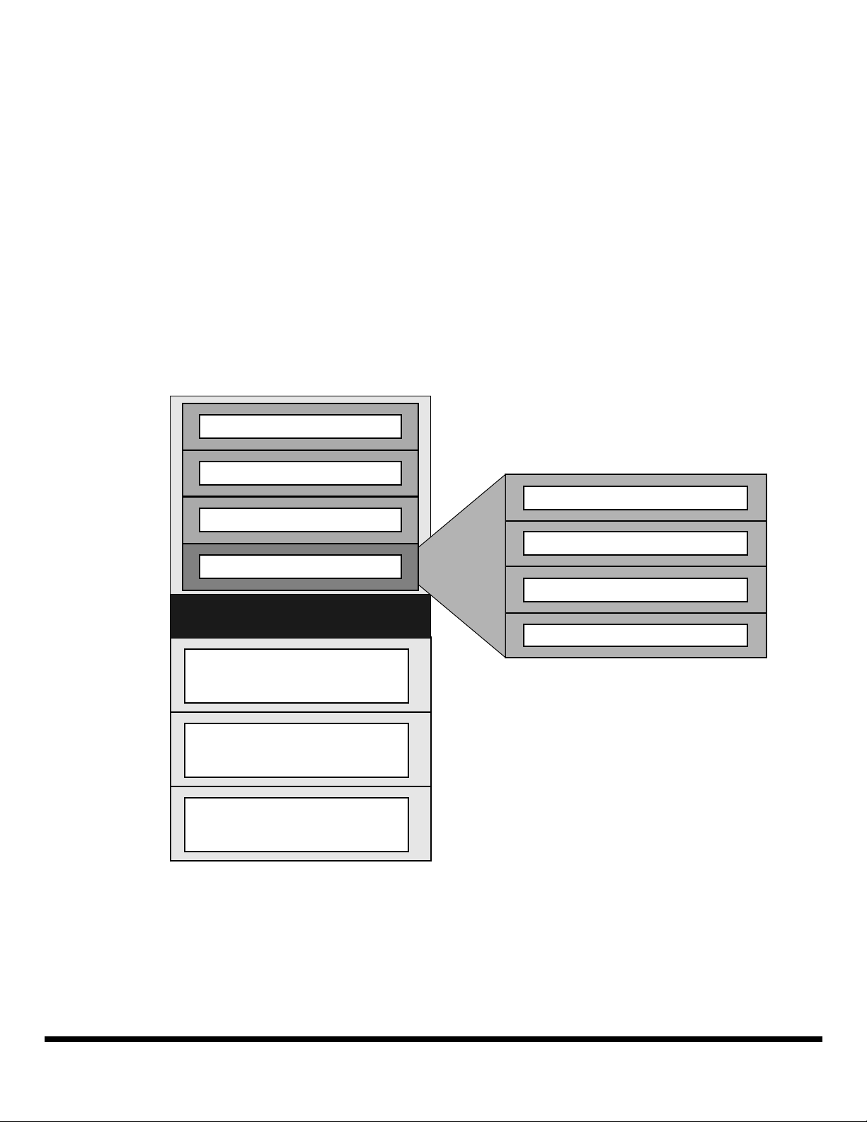
Utopia
I/F
Host
System
Utopia
I/F
Ingress PHY I/F (IPHI)
MultiPhy Support
Microprocessor I/F
(MPIF)
Egress PHY I/F (EPHI)
MultiPhy Support
Ingress Cell Processor
(IPU)
External Memory I/F
(EMIF)
Internal SCAN
(ISCAN)
Egress Cell Processor
(EPU)
FMC Generation
(FMC)
Figure 1. Representative Block Diagram
This document contains information on a new product. Specifications and information herein are subject to change
without notice.
MOTOROLA, INC. 1997
REV 1.1
Ingress Switch I/F
(ISWI)
JTAG
Boundary
Scan
Egress Switch I/F
(ESWI)
Utopia
I/F
Memory
I/F
Test
Port
Utopia
I/F

TABLE OF CONTENTS
1. ATM NETWORK
1.1 ATM Network Description ................................... 3
1.2 ATM Network Applications ................................. 4
2. FUNCTIONAL DESCRIPTION
2.1 System Functional Description .......................... 5
2.2 MC92500 Functional Description ....................... 5
2.2.1 Ingress Cell Flow ......................................... 6
2.2.2 Egress Cell Flow .......................................... 6
2.3 Other Functions ................................................. 7
2.4 MC92500 Block Diagram ................................... 7
2.4.1 Ingress PHY Interface (IPHI) ....................... 8
2.4.2 Ingress Cell Processing Unit (IPU) .............. 8
2.4.3 Ingress Switch Interface (ISWI) ................... 8
2.4.4 Egress Switch Interface (ESWI) ................... 8
2.4.5 Egress Cell Processing (EPU) ..................... 8
2.4.6 Egress PHY Interface (EPHI) ....................... 9
2.4.7 External Memory Interface (EMIF) ............... 9
2.4.8 Microprocessor Interface (MPIF) ................. 9
2.4.9 Internal Scan (ISCAN) ................................. 9
2.4.10 Forward Monitoring Cell Generation(FMC) 9
3. REGISTERS DESCRIPTION
3.1 MC92500 Registers ........................................... 9
4. EXTERNAL MEMORY DESCRIPTION
6.2 Interface to Physical Layer - Cell Assembly .....18
6.3 Address Compression ...................................... 19
6.4 Cell Counting .................................................... 19
6.5 Ingress Cell Insertion .......................................20
6.6 Switch Overhead Information ........................... 20
6.7 Transfer to Switch .............................................20
7. EGRESS DATA PATH OPERATION
7.1 Egress Data Path .............................................20
7.1.1 Transfer from Switch ...................................21
7.1.2 Multicast Identifier Translation .................... 22
7.1.3 Egress Cell Insertion .................................. 22
7.1.4 Address Translation .................................... 22
7.1.5 Cell Counting .............................................22
7.1.6 Transmission to Physical Layer .................. 22
8. SYSTEM OPERATION
8.1 MC92500 Modes of Operation......................... 23
8.1.1 Setup Mode ................................................ 23
8.1.2 Operate Mode ............................................23
8.1.3 Reset .......................................................... 23
8.2 Data Path Clock Configuration .........................23
4.1 MC92500 External Memory ............................. 11
4.1.1 Memory Partitioning ................................... 11
5. SIGNAL DESCRIPTION
5.1 Functional Signal Groups ................................. 13
5.2 Ingress PHY Signals ........................................ 13
5.3 Egress PHY Signals ......................................... 14
5.3.1 Ingress Switch Interface Signals ................ 14
5.3.2 Egress Switch Interface Signals ................ 15
5.4 External Memory Signals ................................. 15
5.4.1 Control Signals .......................................... 16
5.4.2 Microprocessor Signals (MP)..................... 16
5.4.3 Clock Signals ............................................. 17
5.4.4 JTAG Interface Test Signals ....................... 17
6. INGRESS DATA PATH OPERATION
6.1 Ingress Data Path ............................................ 17
9. ELECTRICAL CHARACTERISTICS
9.1 Electrical Specifications ...................................24
9.1.1 Clocks ........................................................ 24
9.1.2 Microprocessor Interface Timing................ 25
9.1.3 PHY Interface Timing .................................32
9.1.4 Switch Interface Timing .............................. 33
9.1.5 External Memory Interface Timing............. 34
9.1.6 Write Cycle Timing ..................................... 34
9.1.7 Read Cycle Timing ..................................... 35
9.1.8 DC Electrical Characteristics .....................36
10. PACKAGE INFORMATION
10.1 Pin Assignment .............................................. 38
10.2 256 PBGA Case Outline .................................39
MOTOROLA MC92500
2

1. ATM NETWORK
1.1 ATM Network Description
A typical ATM network consists of user end stations
that transmit and receive 53-byte data cells on virtual
connections (see Figure 1). The virtual connections are
implemented using physical links and switching systems that interconnect them. The specific combination
of physical links that implements a virtual connection is
chosen when the connection is established. On a given
physical link, each connection is assigned a unique
connection identifier. The connection identifier is
placed in the header of each cell by the transmitting
equipment and is used by the receiving equipment to
route the cell to the next physical link on the connection
path. All cells belonging to a specific virtual connection
follow the identical path from the transmitting end station through the switching systems to the receiving end
station.
Each switching system handles multiple physical links
and transfers each arriving ATM cell from its source link
to its destination link according to the pre-arranged
routing for the connection to which the cell belongs. The
switching system consists of a switch fabric, which handles the actual routing of the cells, and a line card for
each physical link (or group of links) to interface between the physical medium and the switch fabric. The
line card recovers incoming cells from the arriving bit
stream and converts outgoing cells into a bit stream for
transmission.
ATM standards divide the tasks to be performed on
each side of the switch fabric into PHY-layer and ATMlayer tasks. The PHY-layer tasks are dependent on the
physical medium used to connect the switching
systems, while the ATM-layer tasks operate at the cell
level and are independent of the physical medium.
Therefore, it is logical to implement the PHY-layer and
ATM-layer functions on separate devices. In this case
the line card appears as in Figure 2. There are one or
more PHY-layer devices, an ATM-layer device, and
clock recovery devices to clock the PHY devices in
accordance with the signals arriving on the physical
media.
End
Stations
Switch
Clk Rec
Switch
Line
Card
PHY
Switch
Switch Switch Switch
Switching Fabric
MC92500
ATM Layer Functions
Switch
Line Card
VCsVCs
End
Stations
Line
Card
Figure 2. MC92500 in an ATM Network Application
MC92500 MOTOROLA
3

1.2 ATM Network Applications
The MC92500, an Asynchronous Transfer Mode cellprocessing device, is ideally suited for use in the interface between a PHY-layer device and an ATM switch
fabric. The primary application of the MC92500 is ATMlayer cell processing and routing.
Figure 3 illustrates a typical ATM line card using the
MC92500 device. The MC92500 uses an external
memory for storing the ATM virtual connections of the
cells it processes. In addition, the MC92500 offers an
option to utilize an external address compression device accessed via the same external memory bus.
The microprocessor is used for configuration, control
and status monitoring of the MC92500 and is responsible for initializing and maintaining the external memory.
The MC92500 is the master of the external memory
bus. At regular intervals the MC92500 allows the microprocessor to access the external memory for updating
and maintenance.
System RAM can also be located on the line card. The
MC92500 can support a DMA device to allow efficient
data transfer to this RAM without processor intervention.
The physical interface (PHY-IF) implements the physical layer functions of the B-ISDN Protocol Reference
Model.This includes the physical medium dependent
functions required to transport ATM cells between the
ATM user and the ATM switch (UNI) or between two
ATM switches (NNI). The cells are transferred between
the physical interface and the MC92500 using the
UTOPIA standard.
The MC92500 implements B-ISDN UNI/NNI ATM-layer
functions required to transfer cells to and from the
switch over virtual connections. These functions
include usage enforcement, address translation, and
Operation and Maintenance (OAM) processing.The
MC92500 provides context management for up to 64K
Virtual Connections (VCs). The VCs can be either
Virtual Path Connections (VPCs) or Virtual Channel
Connections (VCCs). ATM cells belonging to a
particular VCC on a logical link have the same unique
Virtual Path Identifier/Virtual Channel Identifier,
(VPI/VCI) value in the cell header. Similarly, cells
belonging to a particular VPC on the same logical link
share a unique VPI.
RAM
RAM
LINE CARD
Microprocessor
Bus
Clock
Recovery
µP
µP
PHY-IF
PHY-IF
PHY-IF
DMA
DMA
MC92500
Figure 3. Typical MC92500 Line Card Application
External
Ext-MEM
Memory
External
Memory
Bus
External
Ext
Address
Addr
Compression
Comp
to switch
from switch
MOTOROLA MC92500
4

2. FUNCTIONAL DESCRIPTION
2.1 System Functional Description
A serial transmission link operating at up to 155.52Mbit/
sec (PHY) is coupled to the MC92500 via a byte-based
interface. The transmission link timing is adapted to the
MC92500 and switch timing by means of internal FIFO
cell buffers. A common clock is used to supply both the
PHY-IF and MC92500.
The host microprocessor initializes and provides realtime control of the data-flow chips (PHY-IF and
MC92500) using slave accesses.
The MC92500 operates in conjunction with an external
connection memory, which provides one context entry
for each active connection. The entry consists of two
types of context parameters: static and dynamic. The
static parameters are loaded into the context memory
when the VC is established, and are valid for the duration of that connection. Included in the static parameters are traffic descriptors, OAM flags and parameters
used by the ATM switch. The dynamic context parameters, which include cell counters, UPC/NPC fields and
OAM parameters, may be modified as cells belonging
to that particular connection are processed by the
MC92500. The microprocessor also accesses the external memory through the MC92500 from time to time
to collect traffic statistics and to update the OAM parameters. During normal cell processing, the MC92500
has exclusive access to the external memory. The context entries for the cells being processed are read and
the updated dynamic parameters are written back. The
MC92500 is responsible for the coherency of the external memory during this time.
At user-programmable intervals the MC92500 provides
the microprocessor with a “maintenance slot”, during
which no cell processing is done, and relinquishes the
external memory bus. The break in cell processing is
made possible by the difference between the MC92500
cell-processing rate and the line rate.
The maintenance slot shall be used by the microprocessor for one or more of the following tasks:
• Connection setup and tear down
• Statistics collection
• Updating OAM parameters of active
connection
The microprocessor is responsible for the coherency of
the external memory at the end of each maintenance
slot.
2.2 MC92500 Functional Description
MC92500 General Features
• Implements ATM Layer functions for Broadband
ISDN according to CCITT recommendations and
ATM forum user network interface specifications
• Provides a throughput capacity of up to 155 Mbit/
sec in each direction
• Processes ATM cells from a SONET STS-3c,
SONET STS-1, DS3 PLCP, or any other physical
link running at up to 155 Mbit/sec
• Optionally supports up to 16 physical links
• Optionally configured as a User Network Interface
(UNI) or Network Node Interface (NNI) on a per-link
basis
• Operates in conjunction with an external memory
(up to 16 MB) to provide context management for
up to 64K Virtual Connections
• Provides explicit bank select signals to support up
to four banks of external memory
• Provides per-connection cell counters with the ability to maintain multiple copies of the counter tables
and dynamically switch between them
• Provides per-link cell counters in both directions
• Provides per-connection Usage Parameter Control
(UPC) or Network Parameter Control (NPC) using
a leaky bucket design with up to four buckets per
connection
• Provides support for Operation and Maintenance
(OAM) Continuity Check function for all connections
• Supports Virtual Path (VP) and Virtual Channel
(VC) level Alarm Surveillance on all connections
using an internal scan process to generate and
insert OAM cells
• Supports OAM Fault Management Loopback test
on all connections
• Supports bidirectional OAM Performance Monitoring on up to 64 connections
• Provides a slave microprocessor interface including a 32-bit data bus
• Provides byte-swapping on cell payloads to and
from the microprocessor bus in order to support
both big-endian and little-endian buses
• Supports cell insertion into the cell streams using
direct access registers which may be written by the
microprocessor or by a DMA device
• Supports copying cells from the cell streams using
direct access registers which may be read by the
microprocessor or by a DMA device
• Supports multicast operation
MC92500 MOTOROLA
5

2.2.1 Ingress Cell Flow
In the Ingress direction, the MC92500 extracts cells
from the FIFO in the PHY. Cell discrimination based on
pre-defined header field values is performed to recognize unassigned and invalid cells. Cell rate decoupling
is accomplished by discarding unassigned cells. Unassigned and invalid cell slots may be used to insert OAM
and messaging cells into the Ingress cell flow. For
VCCs, the 28-bit VPI/VCI address space (32-bit Link/
VPI/VCI if multiple physical links are supported) needs
to be compressed into a 16-bit Ingress Connection
Identifier (ICI). The MC92500 provides a choice of two
methods for performing VCC address compression to
obtain the ICI: a table lookup based on reduced addressing and an external address compression option.
For VPCs, the VPI field is used for a lookup into the
VP Table to obtain the ICI. The ICI is a pointer used to
access the context parameters for the current Ingress
cell from the external context memory. Included in
these parameters are cell counters, UPC/NPC traffic
descriptor, OAM parameters and switch parameters.
The UPC/NPC mechanism entails counting the arriving
cells and, using a flexible arrangement of traffic enforcement algorithms, admitting cells that do not violate
the traffic characteristics established for that connection. Violating cells are tallied and may optionally be
tagged or discarded (removed from the cell flow).
• Provides either a restricted address table
lookup scheme for Ingress address
compression or support for an external address
compression mechanism
• Reads Virtual Connection related UPC/NPC,
OAM and switch context parameters through a
32-bit wide interface to an external memory
• Provides per-connection usage count
• Provides per-connection option to copy cells to
the microprocessor
• Provides per-connection UPC/NPC policing
including detection/counting of violating cells
• Supports OAM continuity check, alarm
surveillance and loopback test on all
connections
• Provides OAM performance monitoring test
capabilities for selected connections
• Supports insertion of cells into the ingress cell
flow
• Optionally performs VPI/VCI translation
• Forwards the received ATM cells to the switch
using a UTOPIA-style interface, optionally
adding associated internal switch context
parameters
• Delay of 3 - 5 cell times from the PHY to the
switch
The OAM flags are used to control when and how OAM
cells are processed and to determine if the current user
cell belongs to a connection that has been selected for
a performance monitoring test. If the Ingress cell belongs to such a connection, the OAM table in external
memory contains the relevant parameters.
Subsequent to the context processing, the Ingress cells
are transferred to the Ingress switch
ally, the associated switch context parameters may be
added to the cell before the header or placed in the VPI/
VCI fields of the header.
Ingress Features
The Ingress section (Ingress refers to cells being transferred from the physical interface to the switch):
• Interfaces to one or more physical interface
chips via an 8-bit wide, parity-protected receive
data bus using the UTOPIA standard
• Decouples PHY timing from switch timing using
independent clocks and a FIFO in the physical
interface
• Performs Ingress cell discrimination based on
pre-assigned ATM cell header values
interface. Option-
2.2.2 Egress Cell Flow
In the Egress direction, the MC92500 receives cells
from the switch along with their associated parameters,
if any. One of these parameters is the Egress Connection Identifier (ECI), which is used for direct lookup into
the context table located in external memory to obtain
the VPI/VCI, cell counters, and OAM flags. If multicast
translation is enabled, the Multicast Identifier (MI) is received from the switch instead of the ECI, and the ECI
is found in the multicast translation table. Cells are subject to processing as indicated by the OAM flags. If the
Egress cell belongs to a connection that has been selected for a performance monitoring test, the OAM Table in external memory contains the relevant
parameters.
The Egress cell header is generated by inserting the
VPI/VCI-field obtained from the Address Translation
Table in the (GFC)/VPI/VCI position and modifying the
PTI-field if and when so indicated by the switch or in
case of an OAM cell. The cell is then forwarded to the
PHY I/F queue. Cell rate decoupling is performed in the
Egress direction, i.e. unassigned cells are optionally
generated if no cells are available from the switch.
MOTOROLA MC92500
6

Egress Features
The Egress section (Egress refers to cells being transferred from the switch to the physical interface):
• Receives ATM cells and associated switch
context parameters (including congestion
notification) from the switch using a UTOPIAstyle interface
• Provides optional multicast identifier to
connection identifier translation
• Reads Egress context parameters from
external memory using direct lookup
• Provides per-connection usage count
• Provides per-connection option to copy cells to
the microprocessor
• Supports OAM continuity check, alarm
surveillance and loopback test on all
connections
• Provides OAM performance monitoring test
capabilities for selected connections
• Supports insertion of cells into the egress cell
flow
• Performs VPI/VCI translation
• Transfers ATM cells to one or more physical
interfaces via an 8-bit wide, parity-protected
transmit data bus using the UTOPIA standard
• Decouples PHY timing from switch timing using
independent clocks and a FIFO in the physical
interface
• Delay of 3 - 5 cell times from the switch to the
PHY
2.3 Other Functions
A general 32-bit slave system interface is provided for
configuration, control, status monitoring, and insertion
and extraction of cells. This interface provides for direct
register access to the MC92500.
The MC92500 is equipped with a standard IEEE
1149.1 boundary scan test logic.
2.4 MC92500 Block Diagram
Figure 4 contains a block diagram of the MC92500. The
individual blocks will be described in this section.
Utopia
I/F
Host
System
Utopia
I/F
Ingress PHY I/F (IPHI)
MultiPhy Support
Microprocessor I/F
(MPIF)
Cell Insertion
Cell Extraction
Configuration Regs.
Maintenance Access
Egress PHY I/F (EPHI)
MultiPhy Support
Ingress Cell Processor (IPU)
VP and VC Address compression
NPC/UPC
Cell Counting
OAM Operations
Add Switch parameters
Microprocessor Cell Insertion
Microprocessor Cell Extraction
External Memory I/F
(EMIF)
Internal SCAN
(ISCAN)
Egress Cell Processor (EPU)
Multicast Translation
Cell Counting
OAM Operations
Address Translation
Microprocessor Cell Insertion
Microprocessor Cell Extraction
FMC Generation
(FMC)
Ingress Switch I/F
(ISWI)
Independent Clock
JTAG
Boundary
Scan
Egress Switch I/F
(ESWI)
Independent Clock
Extract Overhead
Utopia
I/F
Memory
I/F
Test
Port
Utopia
I/F
Figure 4. MC92500 Block Diagram
MC92500 MOTOROLA
7

2.4.1 Ingress PHY Interface (IPHI)
The Ingress PHY Interface (IPHI) block receives cells
on a byte basis from the ATM PHY layer using the
UTOPIA standard interface. It assembles the cells and
synchronizes their arrival to the MC92500 cell processing slots. Unassigned and invalid cells (Table 1 and Ta-
ble 2) are removed to provide cell rate decoupling. Also,
the MC92500 can process cells at a higher rate than
the PHY provides them, thereby creating “holes” in the
cell flow. These can be used for either cell insertion or
for maintenance access (used by the microprocessor to
maintain external memory).
2.4.2 Ingress Cell Processing Unit (IPU)
The Ingress Cell Processing Unit (IPU) operates at a
rate of one cell per cell processing slot. The cell may
have arrived from the IPHI block or may be inserted
from the Microprocessor Interface or Internal Scan
blocks. The Ingress OAM function may also insert PM
Forward Monitoring cells into the Ingress cell flow. A
cell may be inserted when an unused cell slot is available, subject to pacing by a simple leaky bucket algorithm.
The IPU performs address compression on cells that
arrived from the IPHI block in order to associate the cell
with Context Table records in External Memory. The
address compression function detects inactive cells
(cells with no corresponding records in the Context Table).
UPC/NPC is performed on a connection basis or optionally on arbitrary groups of connections. The UPC/
NPC function may detect violating cells as dictated by
the selected UPC/NPC algorithm. Violating cells will
normally be tagged or discarded from the cell flow, but
an option exists to perform the UPC/NPC algorithm for
statistical purposes only without modifying or removing
the cells.
OAM processing is performed where appropriate. The
Ingress OAM function records OAM alarm cells: Alarm
Indication Signal/Remote Defect Indicator (AIS/RDI).
OAM processing for user cells involved in a performance monitoring block test involves computing the
Bit-Interleaved Parity (BIP) and updating the Total User
Cells (TUC) count. For OAM cells the processing may
include overwriting the values of specific fields and
checking or generating the CRC-10 field.
Switch-specific overhead information is read from the
context entry and added to the cell before it is sent on
to the switch interface block. Address translation may
optionally be performed at this point.
The IPU will remove from the cell flow any OAM cell
that has reached its endpoint. Also, certain cells may be
copied to the MPIF for transfer to the microprocessor.
2.4.3 Ingress Switch Interface (ISWI)
The ISWI block contains a cell FIFO. Cells are received
from the IPU. When a full cell has been transferred, the
overhead information needed by the switch (as programmed by the user) is extracted from the internal
data structure along with the ATM header and payload
of the cell. This information is transferred to the switch
at the rate of one byte per clock cycle.
2.4.4 Egress Switch Interface (ESWI)
The ESWI block contains a cell FIFO. Data is received
from the switch at the rate of one byte per clock cycle.
The data structure received from the switch includes
overhead routing information in addition to the ATM
cell. When a full cell has been transferred, it is transformed into an internal data structure and presented to
the EPU for processing.
2.4.5 Egress Cell Processing (EPU)
The Egress Cell Processing Unit (EPU) operates at the
rate of one cell per cell processing slot. The cell may
arrive from the Egress Switch Interface Block or may be
inserted from the Microprocessor Interface or Internal
Scan Blocks. The Egress OAM function may also insert
PM Forward Monitoring cells into the Egress cell flow.
The cell insertion is paced by a simple leaky bucket algorithm.
The first stage of the Egress cell processing is performing multicast translation, if needed. Then the EPU performs OAM processing where appropriate. The Egress
OAM function records OAM Alarm cells. OAM processing for user cells involved in a Performance Monitoring
block test is limited to computing the bit-interleaved parity and updating the Total User Cells count. For OAM
cells the processing may include over-writing the values
of specific fields and checking or generating the CRC10 field.
Address translation is performed to replace the address
fields of the ATM cell header with the address of the
outgoing link.The EPU will remove from the cell flow
any OAM cell that has reached its endpoint. Also, certain cells may be copied to the MPIF for transfer to the
microprocessor.
MOTOROLA MC92500
8

2.4.6 Egress PHY Interface (EPHI)
The Egress PHY Interface (EPHI) block takes the processed cells from the EPU, disassembles them into
bytes and transfers them to the physical layer using the
UTOPIA standard interface. Unassigned cells may be
inserted to provide cell rate decoupling.
2.4.7 External Memory Interface (EMIF)
The External Memory Interface (EMIF) block performs
address generation for the MC92500 accesses to the
external memory. It provides 32-bit data and 22-bit address lines along with standard memory control signals.
2.4.8 Microprocessor Interface (MPIF)
The Microprocessor Interface (MPIF) block provides for
configuration of the MC92500, the transfer of cells between the microprocessor and the MC92500, and the
maintenance of external memory. A generic 68xxx compatible 32-bit slave interface is provided for easy
connection to a variety of microprocessor buses. Output signals are provided that can serve as request signals for up to three DMA devices to improve system
performance.
Cells to be inserted in the Ingress or Egress flows are
transferred from the processor memory to an internal
insertion queue.
2.4.9 Internal Scan (ISCAN)
The Internal Scan (ISCAN) block scans the external
memory for connections on which AIS, RDI, or Continuity Check (CC) OAM cells must be inserted. When such
a connection is found, the cells are generated and added to the insertion queue for the cell flow in the appropriate direction.
2.4.10 Forward Monitoring Cell Generation
(FMC)
The Forward Monitoring Cell (FMC) Generation block
keeps track of the connections on which FMCs are
pending during the course of a Performance Monitoring
block test and maintains a priority among them. When
a hole in the cell flow is available, this block requests
the insertion of an FMC on the highest-priority connection.
A cell extraction queue is used to store cells that are directed to the processor. Cells in this queue are transferred first to an internal cell buffer. Then they may be
read by the processor.
3. REGISTERS DESCRIPTION
3.1 MC92500 Registers
The MC92500 registers are divided into several
groups. The register groups are:
Status Reporting Registers - these registers report on
the MC92500 status, and generally may be read and
written by the processor in either of the MC92500
modes of operation (Setup Mode or Operate Mode).
Control Registers - these registers control the
MC92500 operation, and may be read and written by
the processor in either of the MC92500 modes of operation (Setup Mode or Operate Mode).
Configuration Registers - these registers are used to
define the MC92500 configuration, and may be read by
the processor in either of the MC92500 modes of operation (Setup Mode or Operate Mode). These registers
may be written by the processor only in Setup Mode of
operation.
Cell Insertion Registers - these registers are used for
cell insertion into the MC92500 cell flow, and may be
written by the processor when the MC92500 is in Operate Mode. In order to improve performance, the
MC92500 Cell Insertion Registers receive special treatment and may be accessed without wait states.
Cell Extraction Registers - these registers are used for
copying cells from the MC92500 cell flows, and may be
read by the processor when the MC92500 is in Operate
Mode. In order to improve performance, the MC92500
Cell Extraction Registers receive special treatment and
may be accessed without wait states.
Pseudo Registers - these registers are used to perform
certain operations on the MC92500, and may be written
by the processor in either of the MC92500 modes of operation (Setup Mode or Operate Mode).
MC92500 MOTOROLA
9
External Address Compression Device - this memory
space may be used by the processor to access the external address compression device. The External
Address Compression Device may be accessed when
the MC92500 is in Setup Mode or during maintenance
slots.
External Memory - this memory space may be used by
the processor to access the External Memory. If the “De-
ADD (25:0)
0000000
Cell Insertion
0010000
Alt. Cell Insertion
0020000
Cell Extraction
0030000
General Registers
0030FFF
structive” memory space is used, the MC92500 will automatically provide a write-back of zeros to each
External Memory location that is read. The External
Memory may be accessed when the MC92500 is in Setup Mode or during maintenance slots.
Figure 5 presents the MC92500 memory space addres-
sable by the microprocessor using the MADD bus.
Status Reporting
Control Registers
Configuration Registers
1000000
2000000
3000000
3FFFFFF
Pseudo Registers
External Address
Compression Device
External Memory
(Non-“Destructive”)
External Memory
(“Destructive”)
Figure 5. MC92500 Processor Memory Map
MOTOROLA MC92500
10

4. EXTERNAL MEMORY DESCRIPTION
4.1 MC92500 External Memory
The MC92500 uses external memory to store the database (context information) relating to the processing of
cells on a per-connection basis. The MC92500 can access External Memory with 16- or 32-bit data.
4.1.1 Memory Partitioning
The External memory is partitioned into several tables:
(see Figure 6)
• Ingress Billing Counters - consists of a record for
each active connection. The record contains the
cell counters that are used by the connection during the normal Ingress cell flow. This table is dynamic and updated by the MC92500. The
microprocessor is responsible for collecting the
contents of the counters on a regular basis.
• Egress Billing Counters - consists of a record for
each active connection. The record contains the
counters that are used by the connection during the
normal Egress cell flow. This table is dynamic and
updated by the MC92500. The microprocessor is
responsible for collecting the contents of the
counters on a regular basis.
Flags Table - consists of a record for each active
•
connection. The record contains OAM flags that
are used by all the connections during the normal
cell flow. This table is dynamic and updated by the
MC92500
checking the flags on a regular basis
• Context Parameters Table - consists of a record for
each active connection. The record contains connection-specific information for processing and
routing the cells belonging to the connection.
• Ingress Policing Counters - consists of a record for
each active connection. The record contains the
counters that are used to record the results of the
UPC/NPC policing. This table is dynamic and updated by the MC92500. The microprocessor is responsible for collecting the contents of the counters
on a regular basis.
. The microprocessor is responsible for
• VC Table - contains a list of all the Ingress Connection Identifiers (ICIs) that have been defined by the
microprocessor as active Virtual Channel Connections. This table exists only if the Table Lookup
method of Address Compression is used with VC
Table Lookup enabled.
• Multicast Translation Table - contains the Egress
Connection Identifiers (ECIs) associated with the
multicast identifiers.
• OAM Table - contains the additional information
required to run OAM Performance Monitoring.
• VP Table(s) - each record contains an Ingress Connection Identifier (ICI) that has been defined by the
microprocessor as an active connection. The size
and location of the VP Table(s) are determined by
the Link Register. If multiple links are supported,
each Link Register defines a separate VP Table.
The multiple VP Tables are not required to be contiguous.
• Dump Vector Table - contains the dump vectors
describing the recent history of the cell processing.
This table is generally only used for debugging
purposes.
• Egress Link Counters - consists of a record for
each link. The record contains the cell counters that
are used by the link during the normal Egress cell
flow. This table is dynamic and updated by the
MC92500. The microprocessor is responsible for
collecting the contents of the counters on a regular
basis.
• Ingress Link Counters - consists of a record for
each link. The record contains the cell counters that
are used by the link during the normal Ingress cell
flow. This table is dynamic and updated by the
MC92500. The microprocessor is responsible for
collecting the contents of the counters on a regular
basis.
• Virtual Bucket Table - each record in this table contains the information for the UPC/NPC enforcement. This is not a physical table, but a virtual one.
Since the Parameters Table contains a full address
for the location of the Bucket record of each connection, there is no need to put all the Bucket
records in consecutive physical locations. Although
the user can distribute the records in any manner.
MC92500 MOTOROLA
11

Ingress Billing Counters Table pointer
Egress Billing Counters Table pointer
Flags Table pointer
Context Parameters Table pointer
Ingress Policing Counters Table pointer
VC Table pointer
32 bits
Ingress Billing
Counters Table
Egress Billing
Counters Table
Flags Table
Context
Parameters Table
Ingress Policing
Counters Table
Multicast Table pointer
OAM Table pointer
VP Table pointer
Dump V ector Table pointer
Egress Link Counters Table pointer
Ingress Link Counters Table pointer
Bucket pointer
Figure 6. External Memory Partitioning
VC Table
Multicast Table
OAM Table
VP Table(s)
Dump V ector Table
Egress Link
Counters Table
Ingress Link
Counters Table
Virtual Bucket Table
MOTOROLA MC92500
12

5. SIGNAL DESCRIPTION
5.1 Functional Signal Groups
This section contains brief descriptions of the input and
output signals in their functional groups, as shown in
Figure 7. Each signal is explained briefly.
CONTROL
PROCESSOR
INTERFACE
INGRESS
PHY
INTERFACE
EGRESS
PHY
INTERFACE
ENID
AMODE(0-1)
MCLK
MADD(2-25)
MWR
MSEL
MDS
MWSH
MWSL
MDTACK
MDATA(0-31)
MINT
MCIREQ
MCOREQ
EMMREQ
RXDATA(0-7)
RXPRTY
RXSOC
RXEMPTY
RXENB
RXPHYID(0-3)
TXFULL
TXDATA(0-7)
TXPRTY
TXSOC
TXENB
TXCCLR
TXPHYID(0-3)
TXPHYIDV
MC92500
5.2 Ingress PHY Signals
The following signals relate to the PHY interface that is
connected to the PHY chip(s) using the UTOPIA standard. All of the input signals are sampled at the rising
edge of ACLK, and all of the output signals are updated
at the rising edge of ACLK.
ACLKARST
TESTSEL
TESTOUT
VCOCTL
EMDATA(0-31)
EMADD(2-23)
EMWR
EMBSH(0-3)
EMBSL(0-3)
EACEN
SRXDATA(0-7)
SRXPRTY
SRXSOC
SRXCLAV
SRXENB
SRXCLK
STXCLAV
STXDATA(0-7)
STXPRTY
STXSOC
STXENB
STXCLK
TCK
TMS
TDI
TRST
TDO
CLOCK
EXTERNAL
MEMORY
INTERFACE
INGRESS
SWITCH
INTERFACE
EGRESS
SWITCH
INTERFACE
JTAG
INTERFACE
Figure 7. Functional Signal Groups
MC92500 MOTOROLA
13

Receive Data Bus (RXDATA0 - RXDATA7)
This input data bus receives octets from the PHY
chip. When RXENB
the MC92500.
Receive Data Bus Parity (RXPRTY)
This input is the odd parity over RXDATA. This input is ignored if RXENB was not active or the parity
check is disabled.
Receive Start Of Cell (RXSOC)
This input, when high, indicates that the current
RXDATA is the first byte of a cell. This input is sampled
when RXENB
Receive PHY Empty (RXEMPTY
This input, when low, indicates that currently the
PHY chip has no available data.
Receive Enable (RXENB
This output, when low, indicates that the MC92500
is ready to receive data.
Receive PHY ID (RXPHYID0 - RXPHYID3)
This input bus indicates the ID number of the PHY
device currently transferring data to the MC92500. If
only a single PHY device is supported, this bus should
be tied low. This bus is sampled along with the first octet of each cell.
is active, RXDATA is sampled into
is active.
)
)
5.3 Egress PHY Signals
Transmit Start Of Cell (TXSOC)
This output signal indicates, when high, that the
current data on TXDATA is the first byte of a cell.
TXSOC is valid when TXENB
Transmit PHY Full (TXFULL
This input signal indicates, when low, that the PHY
device is full.
Transmit Cell Clear (TXCCLR
This input signal indicates, when low, that the current cell should be cleared from the Egress PHY interface.
Transmit PHY ID (TXPHYID0 - TXPHYID3)
This output bus indicates the ID number of the
PHY device to which either the current cell or the next
cell is directed.
Transmit Next PHY ID Valid (TXPHYIDV
This output signal, when low, indicates that TXPHYID (when configured as the next cell’s ID) is valid.
If TXPHYID is configured to refer to the current cell,
TXPHYIDV
is not used.
is asserted.
)
)
)
5.3.1 Ingress Switch Interface Signals
The following signals relate to the Ingress switch interface. All of the input signals are sampled at the rising
edge of SRXCLK, and all of the output signals are updated at the rising edge of SRXCLK.
The following signals relate to the PHY interface that is
connected to the PHY chip(s) using the UTOPIA standard. All of the input signals are sampled at the rising
edge of ACLK, and all of the output signals are updated
at the rising edge of ACLK.
Transmit Data Bus (TXDATA0-TXDATA7)
This output data bus transmits octets to the PHY
chip. When TXENB is active, TXDATA contains a valid
octet for the PHY.
Transmit Data Bus Parity (TXPRTY)
This output signal is the odd parity over TXDATA.
When TXENB
the PHY.
Transmit Enable (TXENB
This output signal, when low, indicates that
TXDATA, TXPRTY, and TXSOC are valid data for the
PHY.
MOTOROLA MC92500
14
is active, TXPRTY is a valid parity bit for
)
Receive Clock (SRXCLK)
This input signal is used to clock the ingress switch
interface signals.
Receive DATA BUS (SRXDATA0-SRXDATA7)
This 3-state output data bus transmits bytes to the
switch. When SRXENB
valid data for the switch. This bus is updated on the rising edge of SRXCLK.
Receive Data Bus Parity (SRXPRTY)
This 3-state output is the parity protection of SRXDATA transmitted to the switch. It is output on the rising
edge of SRXCLK.
is active, SRXDATA contains

Receive Start Of Cell (SRXSOC)
Transmit Cell Available (STXCLAV)
This 3-state output, when high, indicates that the
current data on SRXDATA is the first byte of a cell
structure (including the overhead bytes). It is output on
the rising edge of SRXCLK.
Receive Switch Cell Available (SRXCLAV)
This output, when asserted, indicates that the
MC92500 has a cell ready to transfer to the switch.
When negated, it indicates that currently there is no
data available for the switch. It is output on the rising
edge of SRXCLK.
Receive Enable (SRXENB
This input, when low, enables new values on SRXDATA, SRXPRTY and SRXSOC. This input is sampled
on the rising edge of SRXCLK.
)
5.3.2 Egress Switch Interface Signals
The following signals relate to the Egress switch interface. All of the input signals are sampled at the rising
edge of STXCLK, and all of the output signals are updated at the rising edge of STXCLK.
Transmit Clock (STXCLK)
This input signal is used to clock the egress switch
interface signals.
Transmit Data Bus (STXDATA0 - STXDATA7)
This input data bus receives bytes from the switch.
When STXENB
the MC92500 on the rising edge of STXCLK.
Transmit Data Bus Parity(STXPRTY)
This input is the parity over STXDATA. This input
is ignored if STXENB
disabled. It is sampled on the rising edge of STXCLK.
is asserted, STXDATA is sampled into
is negated or the parity check is
This output, when asserted, indicates that the
MC92500 is prepared to receive a complete cell. It is
output on the rising edge of STXCLK.
5.4 External Memory Signals
The following signals relate to the External memory interface.
External Memory Data Bus (EMDATA0-EMDATA31)
This three-state bidirectional bus provides the
data path between the MC92500 and the External
Memory.
External Memory Address Bus (EMADD2EMADD23)
This output bus provides the general address bus
which is used by the MC92500 in its accesses to the
External Memory.
External Memory Write (EMWR
This output signal indicates that the current cycle
to the External Memory is a write cycle. This signal is
active low and is asserted within the cycle.
External Memory Bank Select High (EMBSH0
EMBSH3)
These output signals are used to select the high
word of the appropriate memory bank. One or more of
these signals is asserted for each External Memory access according to the value of EMADD. During a maintenance write access from the microprocessor, the
value detected on MWSH
EMBSH signal. These signals are active low.
External Memory Bank Select Low (EMBSL0
EMBSL3)
is driven on the appropriate
)
-
-
Transmit Start Of Cell (STXSOC)
This input indicates, when high, that the current
data is the first byte of a cell structure (including the
overhead bytes). This input is sampled on the rising
edge of STXCLK when STXENB
Transmit Enable (STXENB
This input, when low, enables
STXDATA, STXPRTY, and STXSOC. It is sampled on
the rising edge of STXCLK.
MC92500 MOTOROLA
is asserted.
)
These output signals are used to select the low
word of the appropriate memory bank. One or more of
these signals is asserted for each External Memory access according to the value of EMADD.During a maintenance write access from the microprocessor, the
value detected on MWSL
EMBSL signal. These signals are active low.
External Address Compression Enable (EACEN
This output signal is asserted when data is being
written to or read from an external address compression device using the External Memory Data Bus. This
signal is active low.
is driven on the appropriate
)
15

5.4.1 Control Signals
MP Write (MWR
)
These signals are used to control the MC92500.
ATMC Power-Up Reset (ARST
This input signal is used for power-up reset of the
entire chip. It must be asserted for at least the time required by the PLL to lock.
Enable IDD (ENID)
This input is a dedicated test signal which must be
grounded during normal system operation.
ATMC Mode (AMODE0-AMODE1)
These inputs are dedicated test signals which
must be grounded during normal system operation.
)
5.4.2 Microprocessor Signals (MP)
The following signals relate to the microprocessor
interface.
MP Clock (MCLK)
This input signal is used as the Microprocessor
clock inside the MC92500. This signal drives the microprocessor interface logic in the MC92500. The duty cycle should be in the range of 40-60%.
MP Data Bus (MDATA0-MDATA31)
This 3-state bidirectional bus provides the general
data path between the MC92500 and the microprocessor.
MP Address Bus (MADD2-MADD25)
This input bus contains the address which is used
by the microprocessor to define the register being accessed. This bus is used by the MC92500 at the assertion of MSEL
MP Select (MSEL
This input signal is used to determine that the current access to the MC92500 is valid. This signal is active low and sampled by the MC92500 on the falling
edge of MCLK.
MP Data Select (MDS
This input signal is used to indicate when the data
on MDATA is valid during a write access to the
MC92500. This signal is active low and sampled by the
MC92500 on the falling edge of MCLK.
and sampled on the falling edge of MCLK.
)
)
This input signal is used to determine whether the
MP is reading from the MC92500 or writing to it. This
signal is active low and sampled by the MC92500 on
the falling edge of MCLK. The MC92500 will drive
MDATA when MSEL
MP Word Select High (MWSH
This input signal indicates that the high word is being accessed. During a maintenance access, the value
detected on MWSH
EMBSH signal. This signal is active low and sampled
by the MC92500 on the falling edge of MCLK.
MP Word Select Low (MWSL
This input signal indicates that the low word is being accessed. During a maintenance write access, the
value detected on MWSL
EMBSL signal. This signal is active low and sampled by
the MC92500 on the falling edge of MCLK.
Note: All Cell Extraction Register, Cell Insertion
Register, and General Register accesses are
long-word (32-bit) accesses, so both MWSH
MWSL should be asserted low for these
accesses.
MP Data Acknowledge (MDTACK
This three-state output signal is used to indicate
when the data on MDATA is valid during a read access
from the MC92500 or when the data has been sampled
during a write access to the MC92500. At the end of
each access, this signal is actively pulled up and then
3-stated (Hi -Z). The user may program the MC92500
not to drive MDTACK
This signal is active low and is output asynchronously
to MCLK.
MP Interrupt (MINT
This output signal is used to notify the microprocessor of the occurrence of interrupting events. This
signal is asserted on the rising edge of ACLK (asynchronous with respect to MCLK).
MP Cell In Request (MCIREQ
This output signal may be used by an external
DMA device as a control line indicating when to start a
new cell insertion cycle into the MC92500. This signal
is asserted whenever the Cell Insertion Register array
is available to be written. This signal is active low and is
output on the falling edge of MCLK.
= 0 and MWR = 1.
)
is driven on the appropriate
)
is driven on the appropriate
and
)
during certain types of accesses.
)
)
MOTOROLA MC92500
16

MP Cell Out Request (MCOREQ)
VCOCTL
This output signal may be used by an external
DMA device as a control line indicating when to start a
new cell extraction cycle from the MC92500. This output is asserted whenever the Cell Extraction Register
array is available to be read. This signal is active low
and is output on the falling edge of MCLK.
External Memory Maintenance Request (EMMREQ
This output signal is asserted a programmable
number of clock cycles before the start of an external
memory maintenance cycle. It is negated after a programmable number of maintenance accesses have
been performed. This signal is active low and is output
on the falling edge of MCLK.
5.4.3 Clock Signals
The following signals are connected to the analog PLL
which is used in the MC92500 ACLK.
ATMC Master Clock (ACLK)
This input signal is used by the PLL to generate the
internal master clock of MC92500. The duty cycle
should be in the range of 40-60%.
TESTSEL
This input is a dedicated test signal which must be
grounded during normal system operation.
TESTOUT
This 3-state output is a dedicated test signal which
must be grounded during normal system operation.
This is a dedicated test signal which must be connected to the analog ground (AVSS) during normal system operation.
5.4.4 JTAG Interface Test Signals
Test Clock (TCK)
)
This input pin is the JTAG clock. The TDO, TDI,
and TMS pins are synchronized by this pin.
Test Mode Select (TMS)
This input pin is sampled on the rising edge of
TCK. TMS is responsible for the state change in the test
access port state machine.
Test Data Input (TDI)
This input pin is sampled on the rising edge of
TCK. TDI is the data to be shifted toward the TDO
output.
Test Data Output (TDO)
This 3-state output pin changes its logical
value on the falling edge of TCK.
Test Reset (TRST
This input pin is the JTAG asynchronous reset.
When asserted low, the test access port is forced to the
Test_Logic_Reset state. When JTAG is not being
used, this signal should be tied to ARST
to GND.
)
or hard-wired
6. INGRESS DATA PATH OPERATION
6.1 Ingress Data Path
The ingress data path includes the following steps:
1. Cell assembly from physical layer
2. Address compression
3. Context Table lookup
4. Cell counting
5. UPC/NPC processing
6. Cell insertion
7. OAM processing
8. Appending switch overhead information and
address translation
9. Transfer to switch
MC92500 MOTOROLA
The cell flow through these steps is shown in Figure 8.
Each step is described in the subsections below. During the processing, the decision can be made to remove a cell from the cell flow based on the connection
parameters or the OAM processing, among other reasons. Such a cell may be copied to the cell extraction
queue.
17

from
µP
CELL
INSR
CNTXT
LKUP
OAM
from PHY layer
IPHI UPC
ADDR
CMPR
Ingress Cell Processing Unit (IPU)
Microprocessor Interface (MPIF)
CNTXT
LKUP
BILLING
CNTRS
Figure 8. Ingress Data Path
6.2 Interface to Physical Layer - Cell
Assembly
The Ingress Physical-Layer Interface (IPHI) block receives cell data from the physical layer using the
UTOPIA standard interface. The bytes are assembled
into cells since the MC92500 processing is on a cell basis. The cells are held in a FIFO and are read one cell
per cell slot by the cell processing block.
The input data pins are parity protected. Parity checking by the MC92500 is optional. When parity checking
is enabled, the MC92500 expects RXPATY to contain
odd parity over RXDATA.
The Header Error Correction (HEC) received from the
SWT
OVRHD
&
ADDR
TRNSL
Cell Extraction Queue
to µ
P
OAM ISWI
physical layer is not checked by the MC92500, and it is
discarded from the cell.
Since the MC92500 processes cells at a higher rate
than they are received from the physical layer, the IPHI
block cannot assemble a cell during every cell processing slot. When no complete cell is available, the IPHI
block informs the Ingress Cell Processing block (IPU),
and a hole is inserted in the cell flow through the
MC92500.
The IPHI block checks the cell header and recognizes
the “unassigned” and “invalid” header values defined in
Table 1 and Table 2.
to switch
Table 1. Pre-assigned Header Values at the UNI
Use GFC VPI VCI PTI CLP
Unassigned cell XXXX 00000000 00000000 00000000 XXX 0
Invalid pattern at the ATM layer XXXX 00000000 00000000 00000000 XXX 1
X= don’t care bit
Table 2. Pre-assigned Header Values at the NNI
Use VPI VCI PTI CLP
Unassigned cell 0000 00000000 00000000 00000000 XXX 0
X= don’t care bit
MOTOROLA MC92500
18

6.3 Address Compression
UPC/NPC
The purpose of the ingress address compression is to
map the address field(s) in the header of the received
cell into a pointer to the entry in the Context Table that
relates to the cell’s virtual connection. The MC92500
supports two types of service, Virtual Path switching
service and Virtual Channel switching service. For VP
switching the address is the Virtual Path Identifier (VPI)
field of the cell header. For VC switching the address
consists of both the VPI and the Virtual Channel
Identifier (VCI) fields of the cell header.
When the MC92500 supports multiple PHY layer
devices, the mapping of ATM addresses to Context
Table entries must be done separately for each PHY
layer link. For this purpose, the number of the link from
which a cell arrived can be treated as an additional address field. In this case, a VP switching address consists of the Link/VPI fields and a VC switching address
consists of the Link/VPI/VCI fields.
Cells that are inactive, i.e. for which no valid connection
is found during address compression, are removed
from the cell flow and copied to the Cell Extraction
Queue.
Address Compression Options
The MC92500 supports two methods for performing
address compression:
1. Table lookup using restricted address spaces
2. External address compression
Table Lookup
When some of the bits of the VPI and/or VCI are not
allocated, the address range can be reduced enough to
make a table lookup scheme practical.
External Address Compression
The external address compression method allows the
user total flexibility in performing the ingress address
compression.
6.4 Cell Counting
If the processed cell was received from the physical
layer (not inserted internally), one of the existing connection cell counters from the Ingress Billing Counters
Table and one of the existing link cell counters from the
Ingress Link Counters Table is incremented. The appropriate counter is chosen based on the CLP bit and
whether the cell is an OAM cell.
One of the major advantages of ATM is the ability to
dynamically distribute the available bandwidth among
many connections. However, it is this feature that
makes congestion in an ATM network difficult to predict. In order to make the network management feasible, limits are imposed on the traffic parameters of each
connection. Typically, the maximum average bandwidth and the maximum burstiness may be defined.
Even when the usage parameters have been defined,
a single user that does not stick to the agreed-upon
parameters can cause congestion which will lead to a
reduction in the quality of service provided to the other
users. Therefore, the usage parameters should be enforced at the entrance to the network in such a way that
the violating user is the one who suffers reduced quality
of service. This enforcement is called Usage Parameter
Control (UPC) at a User-Network Interface (UNI) and is
called Network Parameter Control (NPC) at a NetworkNetwork Interface (NNI).
The MC92500’s UPC/NPC algorithm, based on the
concept of “leaky buckets”, detects cells that violate the
traffic agreement and optionally tags (i.e. changes
CLP-field from 0 to1) or discards (removes from the cell
flow) violating cells. A flexible arrangement of leaky
buckets (0 to 4 per connection), leaky bucket parameters and UPC/NPC enforcement algorithms is provided
for all connections. At connection set-up time a set of
bucket characteristics is loaded into the Bucket Table
section of context memory. This defines the expected
cell arrival pattern on a particular connection, and it is
used by the UPC/NPC function as a means of enforcing
the agreed-upon user traffic.
Note: For constant bit rate and variable bit rate
connections the bucket characteristics are normally defined when the connection is setup and
remain constant. However, other types of connections may require dynamic UPC/NPC enforcers where the processor updates these values
while the connection is active. Caution is advised
when doing so in order to maintain consistency
among the various parameters of the enforcer.
All user data cells that have not been removed from the
cell flow are subject to UPC/NPC processing according
to the parameters of their connection. Counts of the
cells that have been discarded or tagged are optionally
maintained per connection in the Ingress Policing
Counters Table.
MC92500 MOTOROLA
19

A “don’t touch” option is provided to apply the UPC/
NPC algorithm for statistical purposes without tagging
or discarding the violating cells.
A UPC/NPC mechanism can be used to enforce the
sum of several connections. This method is likely to be
used at the boundary point where many VCCs are combined into a VPC.
6.5 Ingress Cell Insertion
The MC92500 makes use of the holes in the cell flow
provided by the IPHI block (whether due to the difference between the cell processing and arrival rates or
the reception of unassigned or invalid cells) to insert
cells into the ingress cell flow. The cell insertion rate is
paced by a single leaky bucket to ensure that the switch
is not flooded with inserted cells beyond its capacity.
The types of cells that can be inserted in the ingress cell
flow are:
6.6 Switch Overhead Information
The MC92500 optionally performs address translation
on the Ingress cell flow. The new address fields are taken from the Ingress Translation Address word of the
Context Parameter Table in the External Memory.
The source of the switch overhead information provided by the MC92500 is the Context Parameters Table
entry for the connection. The overhead bytes are transferred before the cell, most-significant byte first.
of the switch parameter words are not provided, the values of the corresponding overhead bytes added to the
cell are undefined. The MC92500 can add up to 16
bytes of switch overhead information.
If any
6.7 Transfer to Switch
The Ingress Switch Interface (ISWI) block receives
cells from the Cell Processing block, queues them, and
transfers the data structure to the switch.
• OAM cells generated internally by the MC92500
including:
- AIS cells
- RDI cells
- Continuity Check cells
- PM Forward Monitoring cells
• OAM cells generated by the microprocessor
• Other cells generated by the microprocessor
The various types of cells that can be inserted in the ingress cell flow are classified by their insertion priority
and held in separate queues. The insertion priorities
are (from highest to lowest):
1. PM Forward Monitoring cells generated internally by the MC92500
2. Cells from the microprocessor
3. AIS, RDI, and CC cells generated internally by
the MC92500
7. EGRESS DATA PATH OPERATION
7.1 Egress Data Path
The switch interface signals are identical to the
UTOPIA Level 1 Receive Interface with the MC92500
playing the role of the PHY layer and the switch playing
the role of the ATM layer. The switch interface signals
are clocked by an independent clock signal, SRXCLK.
The switch is required to accept cells from the
MC92500 when they are presented on the interface
with a delay of up to one cell slot for synchronization.
Note that the cells may be presented at a higher rate
than they are received from the PHY layer due to cell
insertion. The switch must be capable of receiving the
cells at a sustained rate of one cell per cell slot. Otherwise, the cells may back up in the MC92500, processing will be halted, and cells will not be accepted from
the PHY layer. Although the maximum sustained rate is
one cell per cell slot, the rate can be limited by the insertion pacing mechanism.
The egress data path includes the following steps:
1. Transfer from switch
2. Multicast identifier translation (if necessary)
3. Cell insertion
4. Context Table lookup
5. OAM processing
6. Address translation
MOTOROLA MC92500
20
7. Cell Counting
8. Transmission to the physical layer
The cell flow through these steps is shown in Figure 9.
Each step is described in the subsections below. During the processing, the decision can be made to remove a cell from the cell flow for any of several
reasons. Such a cell may be copied to the Cell
Extraction Queue.

7.1.1 Transfer from Switch
The Egress Switch Interface (ESWI) block contains a
cell FIFO. Data is received from the switch at the rate of
one byte per clock cycle. The data structure received
from the switch includes overhead routing information
in addition to the ATM cell. When a full cell has been
transferred, it is transformed into an internal data structure and presented to the Egress Cell Processing
block.
The switch interface signals are identical to the
UTOPIA Level 1 Transmit Interface with the MC92500
playing the role of the PHY layer and the switch playing
the role of the ATM layer. The switch interface signals
are clocked by an independent clock signal, STXCLK.
The input signal STXSOC is used to delineate the beginning of a cell.
layer and by cell insertion. When the ESWI FIFO is full,
the MC92500 refuses to accept a cell from the switch
by negating STXCLAV.
The number of bytes in the cell data structure received
from the switch is programmable.
The bytes are provided by the switch in the following
order:
1. Overhead bytes
2. ATM Cell Header (4 bytes; PTI, CLP valid; VCI
valid if VP switching)
3. HEC octet (provided only if ESHF is set) - this
octet may be used for overhead information
since no HEC value is stored in the internal data
structure
4. ATM cell payload (48 bytes)
The input data pins are parity protected. If a parity error
is detected on the input pins, the error is reported. If the
parity error occurs on a byte containing any of the overhead fields used by the MC92500 or on a byte of the
cell header, the cell is discarded. If the parity error occurs on a payload byte, the cell is optionally discarded.
If a protocol error is detected on the input pins, the current cell is discarded and the error is reported.
The ESWI block contains a small cell FIFO to assemble
the bytes received from the switch and synchronize the
cells to the cell processing time of the Egress Cell
Processing block. The size of the FIFO is programmable to either 4 or 6 cells. The FIFO is read by the Cell
Processing block at a rate which is limited by the PHY
from µP
from switch
CELL
INSR
ESWI
MULTI-
CAST
TRNSL
CNTXT
LKUP
OAM
CNTXT
LKUP
The fields that are contained in the overhead bytes are:
• Egress Connection Identifier (ECI) / Multicast
Identifier (MI)
• Multicast bit (M)
• Explicit Forward Congestion Indication (EFCI)
• Multicast Translation Table Section (MTTS)
The location of these fields in the overhead, header and
HEC bytes is programmable. Once the valid fields have
been retrieved, the remaining overhead bytes received
from the switch will be discarded since they are of no
use to the MC92500 and are not transferred to the PHY
layer.
to PHY layer
OAM
ADDR
TRNSL
BILLING
CNTRS
EPHI
Egress Cell Processing Unit (EPU)
Cell Extraction Queue
Microprocessor Interface (MPIF)
to µ
P
Figure 9. Egress Data Path
MC92500 MOTOROLA
21

7.1.2 Multicast Identifier Translation
Multicasting involves copying a cell that arrived at the
switch and transmitting it on multiple physical links. In
the general case the ECI of the connection to which the
cell belongs will be different on each link. If the switch
can provide the correct ECI to each MC92500 device,
the multicast operation is transparent to the MC92500.
However, if the switch cannot provide separate ECIs for
each link, a common multicast identifier may be provided to all of the MC92500 devices. Each MC92500 will
translate the multicast identifier into the ECI for its physical link.
7.1.3 Egress Cell Insertion
In order to insert cells into the egress cell flow, the
MC92500 creates holes in the cell flow received from
the switch interface block by not taking a cell from the
FIFO. Inserting many cells in a short period of time may
overload the switch’s queueing capability. Therefore,
the cell insertion rate is regulated by a leaky bucket.
The types of cells that can be inserted in the egress cell
flow are:
• OAM cells generated internally by the MC92500
including:
- AIS cells
- RDI cells
- Continuity Check cells
- PM Forward Monitoring cells
• OAM cells generated by the microprocessor
• Other cells generated by the microprocessor
The various types of cells that can be inserted in the
egress cell flow are classified by their insertion priority
and held in separate queues. The insertion priorities
are (from highest to lowest):
1. PM Forward Monitoring cells generated internally by the MC92500
2. Cells from the microprocessor
3. AIS, RDI, and CC cells generated internally by
the MC92500
7.1.4 Address Translation
The address fields of the cell header are optionally replaced by the outgoing address of the outgoing link as
read from the Egress Translation Address word of the
Context Parameter Table. If the cell belongs to a VPC,
only the VPI field is replaced. If the cell belongs to a
VCC, both the VPI and VCI fields are replaced.
The MC92500 sets the middle bit of the PTI on cells
whose received PTI is 000 or 001 when the EFCI bit received from the Egress switch interface block is set.
7.1.5 Cell Counting
For each cell transmitted to the PHY layer, one of the
counters from the Egress Billing Counters Table for this
connection is incremented, unless the table does not
exist. One of the link cell counters from the Egress Link
Counters Table is also incremented if the table exists.
The appropriate counter is chosen based on the CLP
bit and whether the cell is an OAM cell. Cells that are
removed from the cell flow are not included in the usage
counts. Inserted cells and internally generated cells are
included in the usage counts.
7.1.6 Transmission to Physical Layer
The Egress Physical-Layer Interface (EPHI) block receives cells from the Cell Processing block, queues
them, and transmits the cell data to the physical layer
using the UTOPIA standard interface.
The cells are then stored in a FIFO and are disassembled into bytes for transmission to the physical layer.
The size of the FIFO is programmable to either 2 or 4
cells. If the EPHI FIFO is empty, the MC92500 optionally fills the hole with a cell to provide a continuous cell
flow at the physical layer bit rate. The type of cell used
to fill the holes in either “unassigned” (an ATM layer
cell) or “Idle” (a physical layer cell). If multiple physical
links are supported, the generation of these cells is not
supported and should not be enabled.
Since the MC92500 processes cells at a higher rate
than they are transmitted to the physical layer, the EPHI
block cannot transfer a cell during every cell processing
slot. Over time, cells may accumulate in the EPHI FIFO
until it is full. When this happens, the MC92500 will not
process a cell during the next cell processing slot, allowing the FIFO to drain to the physical layer.
TXPRTY is always driven with odd parity over TXDATA, regardless of whether or not parity checking is enabled on the Ingress PHY Interface.
The fifth octet of the transmitted cell (the HEC field) is
always transmitted as zero, regardless of the value
passed to the MC92500 by the switch interface block.
MOTOROLA MC92500
22

8. SYSTEM OPERATION
8.1 MC92500 Modes of Operation
The MC92500 has two basic modes of operation, Setup and Operate. After reset, the MC92500 is in Setup
Mode. Switching to Operate Mode is accomplished by
writing to a pseudo-register.
8.1.1 Setup Mode
The MC92500 enters Setup Mode after reset. This
mode of operation is used to configure the MC92500
and to initialize the external (context) memory. While in
Setup Mode, the MC92500 does not use the External
Memory, in order to provide the microprocessor and/or
DMA device with unrestricted access to the External
Memory. Additionally, those registers identified as configuration registers may be written only when the
MC92500 is in Setup Mode. A write access to any of
these registers in Operate Mode is forbidden.
When the MC92500 is in Setup Mode, the Receive
PHY Interface is disabled by keeping the RXENB output signal negated. No cells are read from the Egress
switch interface block. The Egress Switch Interface is
disabled by keeping STXCLAV negated. Cell insertion
is not allowed in Setup Mode.
Once the MC92500 has switched from Setup Mode to
Operate Mode, it will not return to Setup Mode until a
hardware or software reset is performed.
8.1.2 Operate Mode
While in Operate Mode, the MC92500 processes the
cells received from the PHY layer and the switch interface block. The configuration registers may be read,
but not written, when the MC92500 is in Operate Mode.
8.1.3 Reset
The MC92500 can be reset in either of two ways: hardware reset by asserting the MC92500 Power-Up Reset
(ARST
Reset Register (SRR). In either case all the internal
registers will be loaded with their default values. The reset process requires 200 ACLK cycles or 200 MCLK cycles, whichever is greater, after the negation of ARST
or the write to the SRR. During this time, writing to the
MC92500 registers is not allowed. At the conclusion of
the reset, the MC92500 will be in setup mode.
When a write access to the SRR is performed, the
MC92500 begins the reset process only after writing
the results of the current cell processing to External
Memory. In this way the External Memory remains consistent, and it is not necessary to re-initialize the External Memory when performing a software reset of the
MC92500.
) pin or software reset by writing to the Software
8.2 Data Path Clock Configuration
The MC92500 is designed such that the PHY data path
interfaces operate using the same clock. The UTOPIA
standard requires the ATM layer to provide the interface clocks, RxClk and TxClk. Since the IPHI and EPHI
interfaces use ACLK, the clock provided to the
MC92500, this same clock should be connected to the
RxClk and TxClk pins of the PHY component.Therefore, these clock signals of the UTOPIA interface are
not explicitly provided by the MC92500. The switch interfaces are independently clocked by the clock signals
connected to the SRXCLK and STXCLK pins. This configuration is shown in Figure 10.
ACLK
RxCLK
PHY
TxCLK
Figure 10. MC92500 Clock Configuration
MC92500 MOTOROLA
IPHI
MC92500
EPHI
ISWI
ESWI
SRXCLK
STXCLK
23

9. ELECTRICAL CHARACTERISTICS
9.1 Electrical Specifications
9.1.1 Clocks
Num Characteristics Min Max Unit
C1 ACLK Cycle Time 39 80 ns
C2 ACLK Pulse Width Low 15 ns
C3 ACLK Pulse Width High 15 ns
C4 ACLK Rise/Fall Time 5ns
C5 MCLK Cycle Time 30 ns
C6 MCLK Pulse Width Low 12 ns
C7 MCLK Pulse Width High 12 ns
C8 MCLK Rise/Fall Time 5ns
C9 SRXCLK/STXCLK Cycle Time 30 ns
C10 SRXCLK/STXCLK Pulse Width Low 12 ns
C11 SRXCLK/STXCLK Pulse Width High 12 ns
C12 SRXCLK/STXCLK Rise/Fall Time 5 ns
C1
C3
ACLK
C4
C4
C5
C7
C2
MCLK
C8 C8
C9
C11
C6
SRXCLK / STXCLK
C12
C12
C10
Figure 11. Clocks Timing
MOTOROLA MC92500
24

9.1.2 Microprocessor Interface Timing
The timing diagrams in this section are intended to con-
vey setup and hold values for input signals and propa-
gation delay values for output signals. The diagrams
are NOT intended to convey cycle based behavior.
Num Characteristics Min Max Unit
1 MSEL
setup time before MCLK falling edge 5 ns
2 MSEL hold time after MCLK falling edge 1 ns
3 MADD/MWR setup time before MSEL assertion 5 ns
4 MADD/MWR hold time after MCLK falling edge
a
3ns
5 MDS setup time before MCLK falling edge 5 ns
6 MDS hold time after MCLK falling edge 1 ns
7 MDATA setup time before MCLK falling edge 4 ns
8 MDATA hold time after MCLK falling edge 1 ns
9 MSEL assertion to MDATA active 0 ns
11 MCLK falling edge to MDATA valid for CER Accesses
b
26 ns
12 MSEL negation to MDATA invalid 1 ns
13 MSEL negation to MDATA inactive 11 ns
14 MWR assertion to MDATA invalid 1 ns
15 MWR assertion to MDATA inactive 11 ns
b
16 MCLK rising edge to MDATA valid for Maintenance Accesses
17 MCLK falling edge to MDATA valid for General Register Accesses
,
c
b
,
d
T
T
ns
D
ns
R
19 MSEL assertion to MDTACK active 0 ns
20 MCLK falling edge to MDTACK inactive 12 ns
21 MSEL assertion to MDTACK asserted
22 MSEL negation to MDTACK negated
23 MCLK rising edge to MDTACK asserted
e
e
e
24 MWSH, MWSL setup time before MCLK falling edge
25 MWSH, MWSL hold time after MCLK falling edge
a
a
9ns
13 ns
13 ns
2ns
3ns
26 MCLK falling edge to REQ valid 0 14 ns
e
27 MCLK falling edge to MDTACK asserted for General Register Read Accesses
28 MCLK falling edge to MDTACK asserted for General Register Write Accesses
29 Access width (MCLK falling edge to MSEL negation) for General Register Write Accesses
,
f
e
,
g
h
T
T
T
RD
WD
W
ns
ns
ns
a. refers only to the first falling edge of MCLK in each access at which MSEL is asserted
b. This is for a 150 pF load. Add 0.9 ns for each additional 10 pF. For a 100 pF load, subtract 4 ns.
c. T
= External Memory access time + 18 ns
D
d. T
= 4 * ACLK period + 20 ns
R
e. This is for a 50 pF load.
f. T
= 4 * ACLK period + 11 ns
RD
g. T
is measured from the MCLK falling edge at which MDS is sampled as asserted. TWD = 4 * ACLK period + 11 ns
WD
h. TW is measured from the MCLK falling edge at which MDS is sampled as asserted. TW = 4 * ACLK period. Note that the setup
and hold times with respect to MCLK (timing values 1 and 2) still apply.
MC92500 MOTOROLA
25

MCLK
MSEL
MADD [25:2]
MWR
1
9
11
2
43
43
15
14
13
12
MDATA [31:0]
21
19
Data Valid
20
22
MDTACK
Figure 12. Cell Extraction Register Read Access Timing
MOTOROLA MC92500
26

MCLK
MSEL
MADD [25:2]
MWR
1
3
9
2
43
4
15
16
12
14
13
MDATA [31:0]
19
23
Data Valid
22 20
MDTACK
Figure 13. Maintenance Read Access Timing
MC92500 MOTOROLA
27

MCLK
MSEL
MADD [25:2]
MWR
1
9
17
2
43
43
15
14
13
12
MDATA [31:0]
27
19 22
Data Valid
20
MDTACK
Figure 14. General Register Read Access Timing
MOTOROLA MC92500
28

MCLK
MSEL
MADD [25:2]
MWR
MWSH/L
24
1
5
2
43
43
25
6
MDS
MDATA [31:0]
7
Data Valid
21
19
8
22
20
MDTACK
Figure 15. Cell Insertion Register Write Access / Maintenance Write Access Timing
MC92500 MOTOROLA
29

MCLK
MSEL
MADD [25:2]
MWR
MWSH/L
24
1
43
43
25
5
29
6
MDS
MDATA [31:0]
7
Data Valid
19 28
8
MDTACK
Figure 16. General Register Write Access Timing
MOTOROLA MC92500
30

MCLK
MCIREQ, MCOREQ, EMMREQ
26
26
Figure 17. DMA Request Signals Timing
MC92500 MOTOROLA
31

9.1.3 PHY Interface Timing
Num Characteristics Min Max Unit
51 setup time before ACLK rising edge 10 ns
52 hold time after ACLK rising edge 1 ns
53 propagation delay from rising edge of ACLK 1 16 ns
ACLK
RXEMPTY
, RXSOC,
RXDATA, RXPRTY,
RXPHYID
RXENB
ACLK
51
53
52
Figure 18. Receive PHY Interface Timing
52
51
TXFULL, TXCCLR
53
TXDATA, TXPRTY,
TXSOC, TXENB,
TXPHYID, TXPHYIDV
Figure 19. Transmit PHY Interface Timing
MOTOROLA MC92500
32

9.1.4 Switch Interface Timing
Num Characteristics Min Max Unit
61 setup time before SRXCLK/STXCLK rising edge 4 ns
62 hold time after SRXCLK/STXCLK rising edge 1 ns
63 propagation delay from rising edge of SRXCLK/STXCLK 1 18 ns
64 SRXCLK rising edge to outputs active 1 ns
65 SRXCLK rising edge to outputs inactive 1 16 ns
SRXCLK
SRXENB
SRXCLAV, SRXSOC,
SRXDATA, SRXPRTY
STXCLK
STXDATA, STXPRTY,
STXSOC, STXENB
61
62
63
64 65
Figure 20. Ingress Switch Interface Timing
62
61
63
STXCLAV
Figure 21. Egress Switch Interface Timing
MC92500 MOTOROLA
33

9.1.5 External Memory Interface Timing
This section represents External Memory timing parameters for the default definition. These values are for
a load of up to 50 pF, which is the rated maximum load
for the External Memory interface pins.
9.1.6 Write Cycle Timing
Num Characteristics Min Max Unit
81 Write Pulse Width
82 EMWR
83 Address Setup Time. EMADD Valid to Beginning of Write
84 Address Valid Time. During this Time EMADD is Valid. 32 ns
85 Address Hold Time. End of Write
87 Data Setup Time. EMDATA Valid to End of Write
88 Data Hold Time. End of Write
a. A write occurs during the overlap of EMBSH0-3, EMBSL0-3, EACEN low and EMWR low.
assertion time. EMWR low to end of Writea.22ns
.16ns
a
a
.6ns
a
to EMADD Invalid. 6 ns
a
.13ns
a
to EMDATA Invalid. 6 ns
81
EMBSH [3:0],
EMBSL [3:0],
EACEN
EMWR
EMADD [23:2]
EMDATA [31:0]
82
84
83 85
8887
Data Valid
Figure 22. External Memory Write Access Timing
MOTOROLA MC92500
34

9.1.7 Read Cycle Timing
Num Characteristics Min Max Unit
90 Enable Pulse Width.
92 Address Setup Time.
93 Address Hold Time. EMADD Invalid to
94 Data Driving Start Point.
95 Data Setup Time. EMDATA Valid to
96 Data Hold Time.
97 Data Driving End Point.
tive
b
EMBSH0-3, EMBSL0-3, EACEN Pulse Width. 28 ns
EMBSH0-3, EMBSL0-3, EACEN High. 33 ns
EMBSH0-3, EMBSL0-3, EACEN High 1
EMBSH0-3, EMBSL0-3, EACEN Low to EMDATA Active. 0 ns
EMBSH0-3, EMBSL0-3, EACEN High.5ns
EMBSH0-3, EMBSL0-3, EACEN High to EMDATA Invalid. 0 ns
EMBSH0-3, EMBSL0-3, EACEN High to EMDATA Inac-
a. A RAM with hold time from address change to data change is required.
b. Failure to meet this value may result in contention on EMDATA if a write access follows.
90
EMBSH [3:0],
EMBSL [3:0],
EACEN
ns
a
9ns
EMWR
93
92
EMADD
97
95
EMDATA [31:0]
94
Data Valid
96
Figure 23. External Memory Read Access Timing
MC92500 MOTOROLA
35

9.1.8 DC Electrical Characteristics
Table 3. Preliminary Electrical Characteristics
ABSOLUTE MAXIMUM RATINGS
Symbol Parameter Value/Value Range Unit
V
DD
4
V
in
Vout
I DC Current Drain per Pin, Any Single Input or Output ±50 mA
I DC Current Drain VDD and VSS Pins ±100 mA
T
stg
T
L
Note: Maximum ratings are those values beyond which damage to the device may occur.
Symbol Parameter Min Max Unit
V
DD
4
V
in
T
A
Notes:
1. All parameters are characterized for DC conditions after thermal equilibrium has been established.
2. Unused inputs must always be tied to an appropriate logic voltage level (e.g., either V
3. This device contains circuitry to protect the inputs against damage due to high static voltages or electric fields; however, it is advised that normal precautions be taken to avoid application of any voltage higher than maximum rated voltages to this high impedance circuit.
4. All input, bidirectional, and MDT
constrained to 0 <
5. SRXDATAx, SRXSOC, SRXPRTY, TDO 3-State outputs must be constrained to 0 <
DC Supply Voltage -0.5 to 3.8 V
DC Input Voltage (5V Tolerant) -0.5 to 5.8 V
4,5
DC Output Voltage -0.5 to V
+ 0.5 V
DD
Storage Temperature -65 to +150 °C
Lead Temperature (10 second soldering) 300 °C
RECOMMENDED OPERATING CONDITIONS (to guarantee functionality)
DC Supply Voltage, VDD = 3.3V (Nominal) 3.0 3.6 V
Input V oltage (5V T olerant) 0 5.5 V
Commercial Operating Temperature 0 70 °C
or VDD).
ss
ACK are 5 V Tolerant. For proper operation it is recommended that Vin and Vout be
(V
in,Vout
) < 5.5 V.
V
< V
out
in Hi-Z State.
DD
MOTOROLA MC92500
36

Table 4. Preliminary DC Electrical Characteristics (Ta = 0˚C to 70˚C) VDD=3.3V±0.3V
Parameter Condition Min. Max. Unit
V
V
I
in
I
OH
I
OL
I
oz
I
DDQ
I
DD
Ci Input Capacitance (TTL) 8 pF
* Inputs may be modified to include pull resistors at any time.
TTL Inputs (5V Tolerant) 2.2 5.5 V
IH
TTL Inputs (5V Tolerant) -0.3 0.8 V
IL
Input Leakage Current,
No Pull Resistor
V
= VDD or V
with Pullup Resistor * -50 -5
in
SS
-5 5
with Pulldown Resistor * 5 50
†
Output High Current,
LVTTL Output Type
Outputs:
EA
CEN, EMWR, EMADDx, EMBSHx, EMBSLx
Output High Current,
LVTTL Output Type
Outputs:
V
=Min
DD
,
VOH Min= 0.8 VDD
-24 -
-4 -
All other outputs
Output Low Current,
LVTTL Output Type
Outputs:
EA
CEN, EMWR, EMADDx, EMBSHx, EMBSLx
Output Low Current,
LVTTL Output Type
Outputs:
V
=Min
DD
,
VOL Max= 0.4 Volts
24 -
4-
All other outputs
Output Leakage Current,
3-State Output
Max Quiescent Supply Current
Output = Hi Impedance
V
= VDD or V
out
= 0mA
I
out
V
= VDD or V
in
SS
SS
-10 10 µA
TBD mA
nominal load capaci-
Max Dynamic Supply Current
tance, ACLK = 25.6Mhz,
TBD mA
MCLK = 33Mhz
µA
mA
mA
MC92500 MOTOROLA
37

10.1 Pin Assignment
10. PACKAGE INFORMATION
Table 5. Functional Pin Assignment
Pack-
age
Pin
C3 TESTOUT A8 MSEL A14 SRXDATA:0 E17 RXDATA:3 J19 EMDATA:18 R19 EMADD:23
A2 ACLK D9 MCIREQ
B2 TESTSEL C9 MCOREQ
D5 MADD:17 B9 MDT
A3 MADD:16 A9 MINT
B4 MADD:15 D10 EMMREQ
C5 MADD:14 C10 MCLK C15 N/C F18 EMDATA:29 L20 EMDATA:12 V20 EMADD:17
A4 MADD:13 B10 MWR
B5 MADD:12 A10 MWSH
C6 MADD:11 A11 MWSL
D7 MADD:10 C11 MDS
A5 MADD:9 B11 SRXENB
B6 MADD:8 A12 SRXDATA:7 D16 RXPHYID:1 G19 EMDATA:23 M17 EMDATA:6 W18 EMADD:11
C7 MADD:7 B12 SRXDATA:6 C17 RXPHYID:0 G20 EMDATA:22 N20 EMDATA:5 V17 EMADD:10
A6 MADD:6 C12 SRXDATA:5 B17 RXPRTY H18 EMDATA:21 N19 EMDATA:4 U16 EMADD:9
B7 MADD:5 D12 SRXDATA:4 C18 RXDATA:7 H19 EMDATA:20 N18 EMDATA:3 Y18 EMADD:8
A7 MADD:4 A13 SRXDATA:3 B20 RXDATA:6 H20 EMDATA:19 P20 EMDATA:2 W17 EMADD:7
C8 MADD:3 B13 SRXDATA:2 C19 RXDATA:5 J17 EA
B8 MADD:2 C13 SRXDATA:1 D18 RXDATA:4 J18 EMWR
V15 EMADD:4 W10 TDO U5 TXPRTY P1 MDATA:25 H2 MDATA:5
U14 EMADD:3 Y9 TDI V4 TXSOC N3 MDATA:24 H3 MDATA:4
Y16 EMADD:2 W9 ENID W4 TXDATA:7 N2 MDATA:23 G1 MDATA:3
W15 N/C V9 STXCLK V3 TXDATA:6 N1 MDATA:22 G2 MDATA:2
Y15 EMBSH:0
W14 EMBSH:1
Y14 EMBSH:2
V13 EMBSH:3
W13 N/C Y7 STXDATA:6 V1 TXDATA:1 L4 MDATA:17 F3 MADD:23
Y13 EMBSL:0
U12 EMBSL:1
V12 EMBSL:2
W12 EMBSL:3
Y12 N/C U7 STXDATA:1 R3 TXPHYID:0
U11 AMODE:1 V6 STXDATA:0 P4 MDATA:31 K2 MDATA:11 D2 VCOCTL
V11 AMODE:0 Y5 STXENB
W11 ARST
Y11 TCK V5 TXFULL
Y10 TRST
V10 TMS Y3 TXPHYID
Signal
Name
Pack-
age
Pin
U9 STXCLAV W1 TXDATA:5 M4 MDATA:21 G3 MDATA:1
Y8 STXSOC V2 TXDATA:4 M3 MDATA:20 F1 MDATA:0
W8 STXPRTY U3 TXDATA:3 M2 MDATA:19 F2 MADD:25
V8 STXDATA:7 T4 TXDATA:2 M1 MDATA:18 G4 MADD:24
W7 STXDATA:5 U2 TXDATA:0 L3 MDATA:16 E1 MADD:22
V7 STXDATA:4 T3 TXPHYID:3 L2 MDATA:15 E2 MADD:21
Y6 STXDATA:3 U1 TXPHYID:2 L1 MDATA:14 E3 MADD:20
W6 STXDATA:2 T2 TXPHYID:1 K1 MDATA:13 D1 MADD:19
W5 TXENB R2 MDATA:29 J2 MDATA:9
Y4 TXCCLR R1 MDATA:27 J4 MDATA:7
Signal
Name
ACK A15 SRXSOC E18 RXDATA:0 K18 EMDATA:15 T20 EMADD:20
Pack-
age
Pin
B14 SRXCLK C20 RXDATA:2 J20 EMDATA:17 P17 EMADD:22
C14 SRXCLAV D19 RXDATA:1 K17 EMDATA:16 R18 EMADD:21
B15 SRXPRTY D20 EMDATA:31 K19 EMDATA:14 T19 EMADD:19
D14 N/C E19 EMDATA:30 K20 EMDATA:13 U20 EMADD:18
A16 RXSOC G17 EMDATA:28 L18 EMDATA:11 T17 EMADD:16
B16 RXENB E20 EMDATA:27 L19 EMDATA:10 U18 EMADD:15
C16 RXEMPTY F19 EMDATA:26 M20 EMDATA:9 U19 EMADD:14
A17 RXPHYID:3 G18 EMDATA:25 M19 EMDATA:8 V18 EMADD:13
A18 RXPHYID:2 F20 EMDATA:24 M18 EMDATA:7 Y19 EMADD:12
T1 MDATA:30 J1 MDATA:10
P3 MDATA:28 J3 MDATA:8
V P2 MDATA:26 H1 MDATA:6
Signal
Name
Pack-
age
Pin
K3 MDATA:12 C1 MADD:18
Signal
Name
CEN P19 EMDATA:1 Y17 EMADD:6
Pack-
age
Pin
R20 EMDATA:0 W16 EMADD:5
Signal
Name
Pack-
age
Pin
Signal
Name
MOTOROLA MC92500
38

10. PACKAGE INFORMATION
256 PBGA Pin Diagram/Power Pin Assignment (Bottom View)
201918171615141312111098
7
6
5
4
3
2
1
A
B
C
D
E
F
G
H
J
K
L
M
N
P
R
T
U
V
W
Y
VDD - D6, D11, D15, F4, F17, K4, L17, R4, R17, U6, U10, U15, B19, B18, C4, D3, W2, Y2, V19, W19, P18, V14
VSS - A1, D4, D8, D13, D17, H4, H17, N4, N17, U4, U8, U13, U17, A19, A20, B3, E4, Y1, W3, Y20, W20, T18, V16
AVDD - C2
AVSS - B1
Block name
MP 67
PHY 34
SWT 26
External memory 64
JTAG 5
General/NC 13
Total Signals 209
NOTE:
Table 6. Signal Pin Allocation
To eliminate coupling of digital switching noise into the PLL through pins AVDD and
AVSS, it is recommended to connect these pins to isolated power and ground.
Table 7. Power Pin Allocation
Number
of pins
Power
VDD 22
VSS 23
AVDD 1
AVSS 1
Total Power 47
Number
of pins
MC92500 MOTOROLA
39

10. PACKAGE INFORMATION
10.2 256 PBGA Case Outline (Preliminary Drawing)
OMPAC - (used for Production) ZP Package
GTPAC - (used for Prototype and Production) ZQ Package
B
-S-
-S-
-
-
A
R
R
-R-
-R-
-
-
K
F
C
0.15 (0.006)
-T-
20 18 16 14 12 10 8 6 4 2
19 17 15 13 11 9 7 5 3 1
A
B
C
D
E
F
G
H
J
K
L
M
N
P
R
T
U
V
W
Y
E
D
0.50 (0.020)
0.50 (0.020)
G
256X O H
M
M
Dimensions for OMPAC Dimensions for GTPAC
MILLIMETERS INCHES
DIM
reflect substrate standardization, consult factory for status.
MIN MAX MIN MAX MIN MAX MIN MAX
A 26.90 27.10 1.0590 1.0669 A 26.90 27.10 1.0590 1.0669
B 26.90 27.10 1.0590 1.0669 B 26.90 27.10 1.0590 1.0669
C 1.330 1.730 0.0523 0.0681 C 1.526 2.134 0.060 0.084
D 1.830 2.430 0.072 0.0956 D 2.026 2.834 0.080 0.112
E 23.80 24.20 0.9370 0.9527 E 17.780 22.860 0.700 0.900
F 23.80 24.20 0.9370 0.9527 F 17.780 22.860 0.700 0.900
G 1.27 BSC .050 BSC G 1.27 BSC .050 BSC
H 0.690 0.810 0.0271 0.0318 H 0.690 0.810 0.0271 0.0318
J 1.335 1.535 .0526 .0604 J 1.335 1.535 .0526 .0604
K 0.310 0.410 0.012 0.016 K 0.510 0.610 0.020 0.024
NOTE:
256 OMPAC package thickness is subject to change to
MILLIMETERS INCHES
DIM
J
S
T
T
R
S
R
S
S
S
S
MOTOROLA MC92500
40

Notes:
MC92500 MOTOROLA
41

Motorola reserves the right to make changes without further notice to any products herein. Motorola makes no warranty, representation or guarantee regarding
the suitability of its products for any particular purpose, nor does Motorola assume any liability arising out of the application or use of any product or circuit, and
specifically disclaims any and all liability, including without limitation consequential or incidental damages. “Typical” parameters can and do vary in different
applications. All operating parameters, including “Typicals” must be validated for each customer application by customer’s technical experts. Motorola does not
convey any license under its patent rights nor the rights of others. Motorola products are not designed, intended, or authorized for use as components in
systems intended for surgical implant into the body, or other applications intended to support or sustain life, or for any other application in which the failure of
the Motorola product could create a situation where personal injury or death may occur. Should Buyer purchase or use Motorola products for any such
unintended or unauthorized application, Buyer shall indemnify and hold Motorola and its officers, employees, subsidiaries, affiliates, and distributors harmless
against all claims, costs, damages, and expenses, and reasonable attorney fees arising out of directly or indirectly, any claim of personal injury or death
associated with such unintended or unauthorized use, even if such claim alleges that Motorola was negligent regarding the design or manufacture of the part.
Motorola and
How to reach us:
USA/EUROPE/Locations not listed: Motorola Literature Distribution; JAPAN: Nippon Motorola Ltd.; Tatsumi-SPD-JLDC,
P.O. Box 20912; Phoenix, Arizona 85036. 1-800-441-2447 or 6F Seibu-Butsuryu-Center, 3-14-2 Tatsumi Koto-Ku, Tokyo 135, Japan. 03-81-3521-8315
602-303-5454
MFAX: RMFAX0@email.sps.mot.com -TOUCHTONE (602) 244-6609 ASIA/PACIFIC: Motorola Semiconductors H.K. Ltd.; 8B Tai Ping Industrial Park,
INTERNET: http://Design-NET.com 51 Ting Kok Road, Tai Po, N.T., Hong Kong. 852-26629298
b are registered trademarks of Motorola, Inc. Motorola, Inc. is an Equal Opportunity/Affirmative Action Employer.
 Loading...