

Page 1

查询MC92314供应商
DVB-T Single Chip Demodulator
Freescale Semiconductor, Inc.
MC92314
nc...
, I
or
emiconduct
eescale S
Fr
Application Note
Authors
Christoph Patzelt (Motorola),
Adrian Turner (NDS)
(Single Chip DVB-T Demodulator)
Rev. 1.3
Date: November 30, 1998 3:37 pm
Motorola reserves the right to make changes without further notice to any products herein. Motorola makes no warranty, representation or guarantee regarding the
suitability of its products for any particular purpose, nor does Motorola a ssume any liability arising out of the application or use of any product or c ircuit, and
specifically disclaims any and all liability, including without limitation consequential or incidental damages. “Typical” parameters which may be provided in Motorola
data sheets and/or specifications can and do vary in different applications and actual performance may vary over time. All operating parameters, including
“Typicals” must be validated for each customer application by customer’s technical experts. Motorola does not convey any license under its patent rights nor the
rights of others. Motorola products are not designed, intended, or authorized for use as components in systems intended for surgical implant into the body, or other
applications intended to support or sustainlife,orforanyotherapplicationinwhich the failure of the Motorola product could create a situation where personal injury
or death may occur. Should Buyer purchase or use Motorola products for any such unintended or unauthorized application, Buyer shall indemnify and hold
Motorola and its officers, employees, subsidiaries, affiliates, and distributors harmless against all claims, costs, damages, and expenses, and reasonable attorney
fees arising out of directly or indirectly, any claim of personal injury or death associated with such unintended or unauthorized use, even if such claim alleges that
Motorola was negligent regarding the design or manufacture of the part. Motorola and are registered trademarks of Motorola, Inc. Motorola, Inc. is an Equal
Opportunity/Affirmative Action Employer.
MOTOROLA, INC. 1997 All Rights Reserved
For More Information On This Product,
Go to: www.freescale.com
Page 2

Freescale Semiconductor, Inc.
Rev. 1.3
Revision Status:
Version 1.2 Finalised.
Summary of Changes or Updates:
• Significant reduction in external intervention.
Rev. 1.1:
• Changes to VCXO LPF included.
Rev. 1.2:
nc...
, I
or
emiconduct
eescale S
Fr
• Added CSE register to OFDM block register map.
• Added AGC Fix and VCXO Fix descriptions.
Rev. 1.3:
• Included performance values and power consumption values.
• Included suggestions to speed up acquisition (AFC Sweep Start, fixing FEC coderate).
• Added Timing Diagram
• Added BGA package information
• Added VCXO tolerance requirement
Trademarks:
For More Information On This Product,
Go to: www.freescale.com
Page 3

nc...
, I
or
emiconduct
eescale S
Fr
Freescale Semiconductor, Inc.
Single Chip DVB-T Demodulator
Table of Contents
Section 1
SYSTEM OVERVIEW
1.1 General Description............................................................................................1-1
1.2 Considerations on Terrestrial Transmission.......................................................1-2
1.2.1 Echoes on the Transmission Path.................................................................1-2
1.2.2 Noise.............................................................................................................1-3
1.3 Advantages of the OFDM Transmission Scheme...............................................1-3
1.4 Overview of the DVB-T System..........................................................................1-4
1.4.1 Modulation Scheme.......................................................................................1-4
1.4.2 OFDM Block..................................................................................................1-6
1.4.3 FFT Block......................................................................................................1-6
1.4.4 Forward Error Correction Block.....................................................................1-6
1.4.4.1 Viterbi Decoder...................................................................................1-6
1.4.4.2 Convolutional Deinterleaver ...............................................................1-7
1.4.4.3 Reed-Solomon Decoder.....................................................................1-7
1.4.4.4 Energy Dispersal Removal (Descrambling)........................................1-7
1.5 References .........................................................................................................1-8
Section 2
PINOUT & SIGNAL DESCRIPTION OF THE MC92314
2.1 Pinout for the 160PQFP Package.......................................................................2-2
2.2 Pinout for the 169BGA Package.........................................................................2-3
2.3 Pin Description of the Single Chip DVB-T Demodulator MC92314....................2-4
Preliminary Information
Section 3
DEVICE DESCRIPTION
3.1 Complete DVB-T Digital Frontend......................................................................3-1
3.2 Component Descriptions ....................................................................................3-1
3.2.1 2K-FFT Processor Block...............................................................................3-1
3.2.2 2K-OFDM Demodulator Block.......................................................................3-2
3.2.2.1 I/Q-Demodulator.................................................................................3-3
Single Chip DVB-T Demodulator - Rev. 1.3 (11/30/98) MOTOROLA
For More Information On This Product,
Go to: www.freescale.com
i
Page 4

nc...
, I
or
Table of Contents
3.2.2.2 Derotator.............................................................................................3-3
3.2.2.3 Time Synchronisation.........................................................................3-3
3.2.2.4 Channel Estimation ............................................................................3-4
3.2.2.5 Channel Estimation RAM ...................................................................3-4
3.2.2.6 Channel Correction.............................................................................3-4
3.2.2.7 Channel State Estimation...................................................................3-4
3.2.2.8 Inner Deinterleaver.............................................................................3-5
3.2.2.9 Symbol Demapper and Bit Deinterleaver ...........................................3-5
3.2.2.10Data Formatter ...................................................................................3-5
3.2.3 FEC Block .....................................................................................................3-6
3.2.3.1 Node Synchroniser.............................................................................3-6
3.2.3.2 Viterbi Error Correction.....................................................................3-12
3.2.3.3 Frame Synchronisation.....................................................................3-18
3.2.3.4 Deinterleaver ....................................................................................3-23
3.2.3.5 Reed-Solomon Decoder...................................................................3-24
3.2.3.6 Descrambler .....................................................................................3-28
Freescale Semiconductor, Inc.
emiconduct
eescale S
Fr
Section 4
DVB-T DEMODULATOR INTERFACES
4.1 General Purpose Outputs...................................................................................4-1
4.2 I2C Interface.......................................................................................................4-1
4.2.1 I2C Functionality............................................................................................4-2
4.2.1.1 Start Condition....................................................................................4-2
4.2.1.2 Stop Condition....................................................................................4-3
4.2.1.3 Transmitting “1” and “0”......................................................................4-3
Preliminary Information
4.2.1.4 Data Transfer Sequence ....................................................................4-3
4.2.1.5 Accessing Registers via I2C...............................................................4-4
4.2.1.6 I2C Interface of the MC92314 ............................................................4-5
4.2.2 I2C Register Maps of the MC92314..............................................................4-7
4.2.2.1 Register Map for the OFDM Part........................................................4-8
4.2.2.2 Register Map for the FEC Part .........................................................4-17
4.3 Tuner Interface .................................................................................................4-25
4.3.1 General Tuner Characteristics ....................................................................4-25
4.3.2 Clock Signals...............................................................................................4-26
4.3.3 Input from the Tuner Analog-to-Digital Converter .......................................4-27
MOTOROLA ANTOC.doc - Rev. 1.3 (11/30/98)
ii
For More Information On This Product,
Go to: www.freescale.com
Page 5

nc...
, I
or
emiconduct
eescale S
Fr
Freescale Semiconductor, Inc.
4.3.4 Tuner Control signals from the MC92314 ...................................................4-27
4.3.4.1 VCXO Control Loop..........................................................................4-28
4.3.4.2 AGC Control Loop ............................................................................4-28
4.4 MPEG-2 Output Interface of the MC92314.......................................................4-28
4.5 References .......................................................................................................4-29
Table of Contents
Section 5
USAGE AND PERFORMANCE OF MOTOROLA’S SINGLE-CHIP DVB-T DEVICE
5.1 Remarks on the Circuit Diagram.........................................................................5-1
5.2 Initialising the Chipset.........................................................................................5-1
5.2.1 Setup of the OFDM Block..............................................................................5-2
5.2.1.1 Registers of the OFDM Block.............................................................5-2
5.3 Monitoring the DVB-T Single Chip......................................................................5-2
5.3.1 Status Information of the OFDM Block..........................................................5-2
5.3.1.1 Hardware pins ....................................................................................5-2
5.3.1.2 Lock Status Registers.........................................................................5-2
5.3.1.3 Usage of the AGC Feedback Register ...............................................5-3
5.3.2 Status Information of the FEC Block.............................................................5-3
5.3.2.1 Hardware Pins....................................................................................5-3
5.3.2.2 Software Registers .............................................................................5-3
5.3.2.3 FEC Block QVAL Values corresponding to BER values ....................5-3
5.4 Performance Considerations..............................................................................5-4
5.4.1 Possible Changes in the OFDM Block..........................................................5-4
5.4.1.1 Speeding up the Acquisition Time......................................................5-4
5.4.1.2 Co-Channel Protection vs. Noise .......................................................5-6
5.4.2 Possible Changes in the FEC Block..............................................................5-6
5.5 MC92314 Performance.......................................................................................5-7
5.5.1 Performance in a typical Consumer Application............................................5-7
5.6 References .......................................................................................................5-10
Preliminary Information
5.4.2.1 Fixing the Coderate for the Viterbi Decoder .......................................5-6
5.4.2.2 Adjusting the MPEG Frame Synchroniser..........................................5-6
5.5.1.1 Typical Lock Performance..................................................................5-7
5.5.1.2 Noise and Interference Performance..................................................5-9
Single Chip DVB-T Demodulator - Rev. 1.3 (11/30/98) MOTOROLA
For More Information On This Product,
Go to: www.freescale.com
iii
Page 6

Table of Contents
Freescale Semiconductor, Inc.
Section 6
ELECTRICAL CHARACTERISTICS
6.1 MC92314 Electrical Considerations....................................................................6-1
6.2 MC92314 DC Electrical Specifications...............................................................6-3
6.3 MC92314 Timing Characteristics........................................................................6-4
Section 7
MECHANICAL CHARACTERISTICS
nc...
, I
or
emiconduct
eescale S
Fr
7.1 Outlines of the 160PQFP Package.....................................................................7-1
7.2 Outlines of the 169BGA Package.......................................................................7-3
Preliminary Information
MOTOROLA ANTOC.doc - Rev. 1.3 (11/30/98)
iv
For More Information On This Product,
Go to: www.freescale.com
Page 7

Freescale Semiconductor, Inc.
System Overview
SECTION 1
SYSTEM OVERVIEW
In this Application Note Motorola’s single chip demodulator and FEC for DVB-T receivers along
with the usual application is described.
This section covers the overall descriptions as well as an introduction into the DVB-T standard,
supporting the understanding of the special features of the OFDM system.
1.1 General Description
Before describing the important specialities of the DVB-T system itself the key features of
Motorola’s single chip are outlined.
nc...
, I
or
emiconduct
eescale S
Fr
• 0.35mm CMOS process at 3.3 V.
• 160 pin QFP package
• 169 BGA package
There are two main sections in the chip, providing the functions necessary to obtain a complete
MPEG-2 transport stream out of one real IF-sampled DVB-T signal. The steps necessary are
OFDM demodulation and FEC decoding, corresponding to the three separate devices
described in Reference [1-4]:
Important capabilities of the FFT/OFDM block:
• Usable for 8 MHz, 7 MHz and 6 MHz channel bandwidth by adjusting the clock rate.
• C/N performance according to Reference [1-1] Annex A with a degradation margin of 3 dB.
• Supported DVB-T modulation schemes: QPSK, 16-QAM and 64-QAM.
• Automatic lock onto all specified guard interval lengths (
• Data input: 8 Bit TTL compatible 2’s complement or offset binary.
• Channel estimation and correction using the pilot carriers.
2
•I
C compatible interface (M-Bus).
Preliminary Information
1
/32,1/16,1/8,1/4).
• Transmission Parameter Signalling (TPS) data is decoded and made available to the
system controller via M-Bus.
• Processing of one block of 2048 complex samples (i.e. one 2K-OFDM symbol) in 224 ms.
• FFT input wordlength 8 bit, output accuracy 12 bit.
• Overflow on certain OFDM subcarriers due to co-channel interferes is prevented internally.
Single Chip DVB-T Demodulator - Rev. 1.3 (11/30/98) MOTOROLA
1-1
For More Information On This Product,
Go to: www.freescale.com
Page 8

Freescale Semiconductor, Inc.
System Overview
Key items of the FEC part include:
• Maximum 37 Mbit/s output rate.
• 3 Bit soft-decision input matched to the output of the OFDM block.
• Code rate
• Automatic or manual rate selection.
• Viterbi decoder survivor depth 96
• Signal quality output data.
• DVB compliant 12 x 17 Forney Convolutional Deinterleaver
• Reed-Solomon (204, 188, 8) decoder as specified by DVB
• DVB Descrambler for Energy Dispersal & inverted Sync Byte removal
1
/2 and depunctured rates of2/3,3/4,5/6, and7/8.
nc...
, I
or
emiconduct
eescale S
Fr
• Bit Error Rate (BER) and uncorrectable Frame Error (BAD) monitoring
• setting of “transport_error_indicator” bit in the MPEG2 output stream (MSB of first byte
immediately following the Sync Byte)
1.2 Considerations on Terrestrial Transmission
Oneof the mostimportant aspectsin designinga transmission systemis tochose themodulation
schemethat fits bestto thecharacteristics ofthe transmission channelemployed. Comparingthe
terrestrial channel in the UHF band with the channels of the satellite or cable system yields
several important differences that exclude the modulation schemes used there from an efficient
usage in the terrestrial channel.
1.2.1 Echoes on the Transmission Path
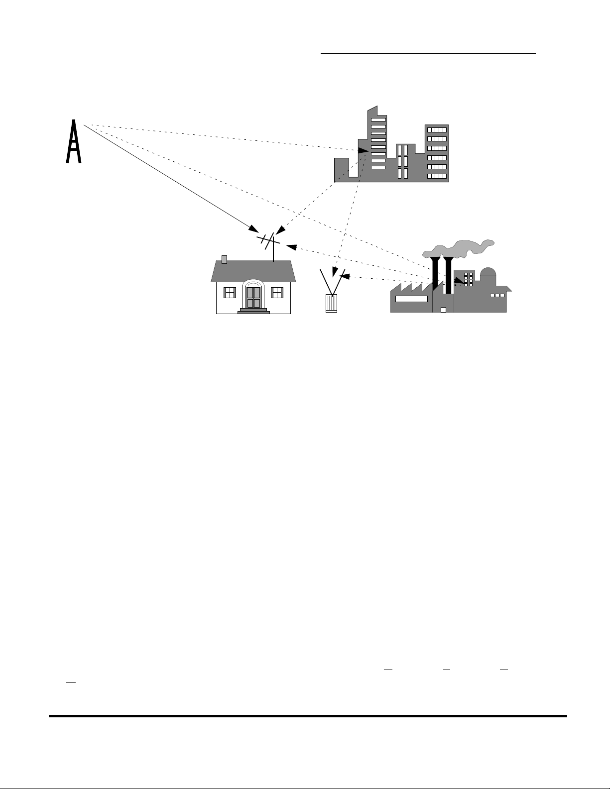
InFigure 1-1 atypical environmentfor terrestrial receptionis given. Theantenna ofthe stationary
receiver receives the signal belonging to the direct path from the transmitter as well as delayed
echoes e.g.from buildings (this iscalled a Ricean channel).In contrast to thisa portable receiver
may receive only echoes without a signal direct from the transmitter (Rayleigh channel
characteristics).
Preliminary Information
MOTOROLA Single Chip DVB-T Demodulator - Rev. 1.3 (11/30/98)
1-2
For More Information On This Product,
Go to: www.freescale.com
Page 9
Freescale Semiconductor, Inc.
System Overview
nc...
, I
or
emiconduct
eescale S
Fr
Figure 1-1. Possible echo constellation
In the well knownanalog TV transmission systems such echoes appear as ghost pictures onthe
screen, but as long as they don’t get too strong the original information remains visible, at the
penalty of reduced picture quality.
1.2.2 Noise
Anotherimpairment on everytransmission channel isthe addition ofnoise. Due tomany reasons
(e.g. thermal noise, impulse noise from ignition sources) the signal quality degrades with
increasing distance from the transmitter. On the analog TV picture the different noise sources
decrease the quality of the picture, but as long as the synchronisation circuitry remains in lock
even heavily distorted pictures deliver visible information to the viewers.
Preliminary Information
1.3 Advantages of the OFDM Transmission Scheme
In contrast to this the behaviour of analog systems outlined in the paragraphs above the
behaviour of digital transmission systems is different. The picture contents are mapped into
digital signals, transmission impairments lead to transmission errors, resulting inbit errors of the
received datastream. Due to the high compression ration of the source encoded MPEG-2
transport stream used in the DVB systems even single bit errors may have a severe impact on
the picture quality. Without careful system layout, taking into account the characteristics of the
transmission channel, the performance of a digital transmission system may be very poor.
The problemsmentioned above canbe circumvented successfully leadingto the presentsystem
for digital terrestrial transmission. One of the main points is the
Multiplex (OFDM)scheme. The following list givesa short overview aboutthe key features of the
DVB-T standard:
Single Chip DVB-T Demodulator - Rev. 1.3 (11/30/98) MOTOROLA
For More Information On This Product,
Go to: www.freescale.com
Orthogonal Frequency Division
1-3
Page 10

nc...
, I
or
emiconduct
eescale S
Fr
Freescale Semiconductor, Inc.
System Overview
• Divide the whole available bandwidth into a large number of subchannels with different
frequencies (Frequency Division Multiplex).
• each subchannel is independent form all others (Orthogonality).
• To combat the echoes in the terrestrial channel a guard interval is used to absorb them.
• Acertain amount ofredundancy isadded tothe bits atthe transmitterside, allowingpowerful
error correction techniques in the receiver.
In principle the whole available bandwidth is divided into a large number N (e.g. 2048) of
separate narrowband subchannels (the OFDM subcarriers). Data transmission on each
subcarrier frequency is independent from and in parallel with the other subcarriers, leading to a
verylow datarate on eachsubcarrier compared tothe overall transmissioncapacity. The splitting
into the subchannels including the modulation onto the subcarriers can be done very efficiently
by performing an
receiver must do a FFT to obtain the original information. Following the usual terms of digital
signal processing the region
is called
before the FFT (in the receiver) is associated with the ‘time domain’.
All these steps together allow the realisation of a robust transmission scheme specially adapted
to the terrestrial channel. Advances in silicon technology enable the implementation of the
advanced signal processing algorithms necessary at costs suitable to the consumer electronics
industry.
Additional information on the OFDM system can be obtained from Reference [1-2] and
Reference [1-3].
‘frequency domain’ and in contrast to it the signal after the IFFT (in the transmitter) until
Inverse Fast Fourier Transform (FFT) to the data to be transmitted. In turn the
before the IFFT in the transmitter and after the FFT in the receiver
1.4 Overview of the DVB-T System
After thorough investigation of the requirements the standard for digital terrestrial television was
finalised in 1996 (see Reference [1-1]). In line with the standards for the satellite system (DVBS) and the cable system (DVB-C) it specifies all the transmission parameters for the
broadcasting of services via terrestrial (e.g. UHF) channels.
Preliminary Information
1.4.1 Modulation Scheme
The standard covers the Orthogonal Frequency Division Multiplex (OFDM) scheme, using
OFDM symbollengths of either 2048(2K) or 8192 (8K) complex-valuedsamples. The integrated
circuit covered in this document can deal only with the 2K-system, so the 8K system is not
covered here.
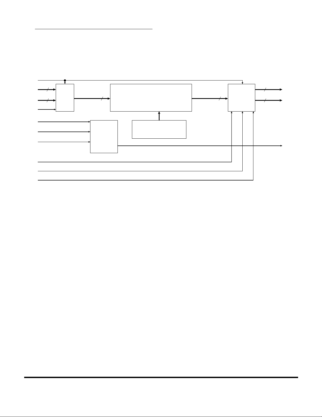
Figure1-2 givesa block diagramof thecomplete DVB-Ttransmission system,theblocks marked
with thick lines are unique to the terrestrial system, whereas the other blocks are identical to the
satellite standard DVB-S. In this diagram also the basic parameters of the transmission
parameters are given, for a more detailed description see Reference [1-1]
MOTOROLA Single Chip DVB-T Demodulator - Rev. 1.3 (11/30/98)
1-4
For More Information On This Product,
Go to: www.freescale.com
Page 11
Freescale Semiconductor, Inc.
Channel
Terrestrial
System Overview
nc...
, I
or
emiconduct
eescale S
Fr
Upconversion
OFDM-Mod.
Frame-Adapt.
and
Mapper
Inner
Preliminary Information
FEC-Encod.
UHF Range
Amplification
Guard-Int.
Modulator
Interleaving
and Interl.
470-862 MHz
2 K IFFT
Pilot insertion
QPSK,
64-QAM,
16-QAM or
72 Bits
with Block size
Bit-Interleaving
Interleaving depth I=12;
RS (204,188) of GF (256)
Different
guard interval
lengths possible
possible
Modulation
Non-uniform
Gray mapping
Symbol
Interleaving
(Frequency)-
,
2
/
1
(G1=171, G2=133),
Convolutional Encoding
Cell memory M=17 byte
8
/
7
,
6
/
5
,
4
/
3
,
3
/
2
Possible Coderates
Mothercoderate
sion I,Q-
Downconver-
Demodulation
OFDM
Synchron.
Demodulation
DemappingInner De-
interleaving
FEC-Decod.
Deinterleaving
15
+x
14
Sync-Inversion
MPEG-2 TS
Scrambling
P(x)=1+x
Descrambling
Sync-Inversion
Figure 1-2. DVB-T transmission system
Single Chip DVB-T Demodulator - Rev. 1.3 (11/30/98) MOTOROLA
1-5
For More Information On This Product,
Go to: www.freescale.com
Page 12

nc...
, I
or
System Overview
Freescale Semiconductor, Inc.
1.4.2 OFDM Block
The OFMD block performs the functions given in the blocks ‘Synchronisation’, ‘Demapping’ and
‘Inner Deinterleaving’ in Figure 1-2. This includes all the necessary synchronisation tasks,
OFDM-related deinterleaving, demapping of the constellation diagram, generation of softdecision information and output formatting. This block is designed to work directly with the FFT
block.
Important capabilities are:
• Usable for 8 MHz, 7 MHz and 6 MHz channel bandwidth by adjusting the clock rate.
• C/N performance according to Reference [1-1] Annex A with a degradation margin of 3 dB.
• Supported DVB-T modulation schemes: QPSK, 16-QAM and 64-QAM.
1
• Automatic lock on all specified guard interval lengths (
• Data input: 8 Bit TTL compatible 2’s complement or offset binary.
• Channel estimation and correction using the pilot carriers.
2
•I
C compatible interface (M-Bus) to the system controller.
/32,1/16,1/8,1/4).
emiconduct
eescale S
Fr
• Transmission Parameter Signalling (TPS) data is decoded and made available to the
system controller via M-Bus.
1.4.3 FFT Block
The FFT block performs the OFDM demodulation in the true sense of the word. It gets the time
domain information from the OFDM block, performs a Fast Fourier Transform on it and delivers
the frequency domain information, i.e. the constellation diagram (suffering from the channel
impairments) back again to the OFDM block.
Main features of the FFT block are:
• Processing of one block of 2048 complex samples (i.e. one 2K-OFDM symbol) in 224 µs.
• FFT input wordlength 8 bit, output accuracy selectable between 10 and 12 bit.
• Overflow on certain OFDM subcarriers due to co-channel interferes is handled internally.
Preliminary Information
1.4.4 Forward Error Correction Block
The FEC part of the DVB-T transmission is located in the blocks ‘FEC-Decoding’,
‘Deinterleaving’, ‘Sync-Inversion’ and Descrambling. All these tasks are handled by the FEC
block. The FEC scheme itself consist of the inner Viterbi decoder and the outer RS decoder.
1.4.4.1 Viterbi Decoder
The Viterbi decoder block is DVB compliant with all the coderates available according to the
specification. Its main features are:
• Maximum 37 Mbit/s output rate.
• Constraint length 7, generator polynomial (171
MOTOROLA Single Chip DVB-T Demodulator - Rev. 1.3 (11/30/98)
1-6
For More Information On This Product,
Go to: www.freescale.com
, 1338)
8
Page 13

nc...
, I
or
Freescale Semiconductor, Inc.
• 3 Bit soft-decision input in suited to the output of the OFDM block.
• Code rate
• Automatic or manual rate selection.
• Programmable internal synchronizer.
• Provision for external synchronization.
• Survivor depth 96
• No internal APLL needed, clock is provided by the OFDM block.
• Signal quality output data.
1.4.4.2 Convolutional Deinterleaver
To achieve the optimal performance of any concatenated coding scheme there must be an
interleaver in the transmitter between the inner and outer encoder. This interleaver distributes
the bytes in a pseudo random order before feeding them into the inner encoder. In turn the
deinterleaver in the receiver rearranges the original order, spreading error bursts provoked by
overloading the inner decoder due to bad channel conditions.
In case of the DVB system the interleaving scheme uses a Convolutional 12x17 Forney
Interleaver: Every 204 bytes of data are interleaved (reordered) at the transmitter and
deinterleaved in the receiver using a Convolutional Deinterleaver with I=12 branches and M=17
byte storage cells as defined by the DVB Specifications.
1
/2 and depunctured rates of2/3,3/4,5/6, and7/8.
System Overview
emiconduct
eescale S
Fr
1.4.4.3 Reed-Solomon Decoder
The FEC block contains a complete Reed-Solomon decoder as specified by DVB for digital
receiver applications (204, 188) of GF(256), that means input blocks with 188 byte in length,
added redundancy of 16 checkbytes leading to 204 bytes output block length. The block will
acceptdata from theViterbi decoderand deliveran MPEG-2 transportstream tothe Set-TopBox
core demultiplexer.
1.4.4.4 Energy Dispersal Removal (Descrambling)
The MPEG-2 data (excluding Sync Bytes) are randomised for Energy Dispersal in the
transmitter. This block reverses the process and re-inverts the inverted Sync Byte prior to
delivering the data to the MPEG-2 Transport Demultiplexer. It is the last step in the frontend
processing chain.
The main features of the deinterleaver, RS decoder and descrambling block are given below:
• 37 MBit/s typical input and output data rates
• optimized Frame Synchronizer performance for DVB parameters
• DVB compliant 12x17 Forney Deinterleaver
• Reed-Solomon (204,188,8) decoder as specified by DVB
• DVB Descrambler for Energy Dispersal & inverted Sync Byte removal
Preliminary Information
Single Chip DVB-T Demodulator - Rev. 1.3 (11/30/98) MOTOROLA
1-7
For More Information On This Product,
Go to: www.freescale.com
Page 14

Freescale Semiconductor, Inc.
System Overview
• setting of “transport_error_indicator” bit in the MPEG2 output stream (MSB of first byte
immediately following the Sync Byte)
• Bit Error Rate (BER) and uncorrectable Frame Error (BAD) monitoring
• 180
o
input data stream phase error correction
1.5 References
[1-1] ETSI (European Telecommunication Standards Institute): Digital broadcasting systems
for television, sound and data services; Framing structure, channel coding and
modulation for digital terrestrial television. Draft prETS 300 744, September 1996.
[1-2] M.Alard, R. Lassalle:Principles ofmodulation and channelcoding for digitalbroadcasting
for mobile receivers. EBU Collected Papers on concepts for sound broadcasting into the
21st century, August 19988, pp. 47-69.
nc...
, I
or
emiconduct
eescale S
Fr
[1-3] J. Gledhill, S. Anikhindi, P. Avon: The transmission of digital television in the UHF band
using Orthogonal Frequency Division Multiplex. Proceedings of the 6th International IEE
Conference on Digital Processing of Signals in Communications, IEEE Conf. Publ.
No. 340, pp. 175-180, September 1991.
[1-4] C. Patzelt, M. Drozd, S. Anikhindi: MC92307 MC92308 MC92309 DVB-T, Chipset
Application Note Version 1.1; Motorola; July 1998.
Preliminary Information
MOTOROLA Single Chip DVB-T Demodulator - Rev. 1.3 (11/30/98)
1-8
For More Information On This Product,
Go to: www.freescale.com
Page 15

Freescale Semiconductor, Inc.
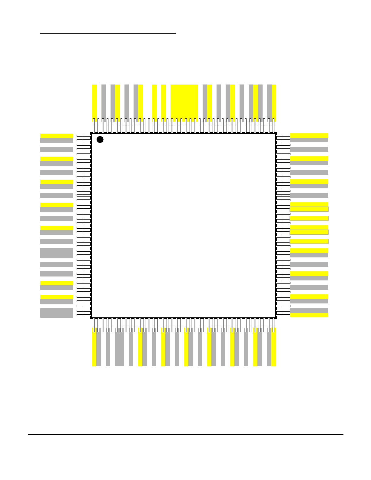
Pinout & Signal Description of the MC92314
SECTION 2
PINOUT & SIGNAL DESCRIPTION OF THE MC92314
Motorola’s DVB-T demodulator is available in a 160QFP package as well as in a 169BGA. The
pinout of this packages as well as the input and output lines are given in Figure 2-1, Figure 2-2
and Table 2-1. The mechanical dimensions of the package are given in Section 7.
The supply voltage of the IC is 3.3 V, its power consumption is app. 1.7 W in a typical DVB-T
application as it is described Section 5.
nc...
, I
or
emiconduct
eescale S
Fr
Preliminary Information
Single Chip DVB-T Demodulator - Rev. 1.3 (11/30/98) MOTOROLA
2-1
For More Information On This Product,
Go to: www.freescale.com
Page 16
Freescale Semiconductor, Inc.
Pinout & Signal Description of the MC92314
2.1 Pinout for the 160PQFP Package
ADCDATA2
VSS
reserved (VSS)
VDD
reserved (VSS)
ADCDATA1
VSS
reserved (VSS)
VDD
reserved (VSS)
ADCDATA0
VSS
VDD
ADCDATA-1
VSS
ADCDATA-2
VDD
INSYNC
VLOCK
TPSLOCKB
reserved (open)
AFCLOCK
CLKLOCK
VSS
reserved (open)
RESB
VDD
reserved (open)
VSS
reserved (open)
TRERROR
VDD
reserved (open)
VSS
reserved (open)
TRSTART
reserved (open)
VDD
reserved (open)
TRVALID
nc...
, I
or
emiconduct
eescale S
ADCDATA3
reserved (VSS)
VSS
reserved (VSS)
VDD
ADCDATA4
reserved (VSS)
VSS
reserved (VSS)
VDD
ADCDATA5
reserved (VSS)
VSS
reserved (VSS)
VDD
ADCDATA6
reserved (VSS)
VSS
reserved (VSS)
VDD
ADCDATA7
reserved (VSS)
VSS
reserved (VSS)
VDD
reserved (VSS)
reserved (VSS)
VSS
reserved (VSS)
VDD
reserved (VSS)
VSS
CLKEN18
reserved (VSS)
VDD
AGCCTLP
reserved (VSS)
VSS
reserved (VSS)
AGCCTLN
140
20
Preliminary Information
160PQFP
60
100
TRCLK
reserved (open)
VSS
reserved (open)
VDD
TRDOUT7
reserved (open)
VSS
reserved (open)
VDD
TRDOUT6
reserved (open)
VSS
reserved (open)
VDD
TRDOUT5
GP3
VSS
GP2
VDD
TRDOUT4
GP1
VSS
GP0
VDD
TRDOUT3
reserved (open)
VSS
reserved (open)
VDD
TRDOUT2
reserved (open)
VSS
reserved (open)
VDD
TRDOUT1
reserved (open)
VSS
reserved (open)
TRDOUT0
Fr
VDD
CLKCTLP
reserved (VSS)
VSS
CLKCTLN
reserved (VSS)
reserved (VSS)
VDD
reserved (VSS)
VSS
SCL
reserved (VSS)
VDD
reserved (VSS)
VSS
SDA
reserved (VSS)
VDD
reserved (VSS)
VSS
CLK
reserved (VSS)
VDD
reserved (VSS)
VSS
MBUSID0
reserved (VSS)
VDD
reserved (VSS)
VSS
MBUSID1
reserved (VSS)
VDD
reserved (open)
VSS
MBUSID2
reserved (open)
VDD
MBUSID3
reserved (open)
Figure 2-1. Pinout for the 160PQFP
MOTOROLA Single Chip DVB-T Demodulator - Rev. 1.3 (11/30/98)
2-2
For More Information On This Product,
Go to: www.freescale.com
Page 17

Freescale Semiconductor, Inc.
Pinout & Signal Description of the MC92314
2.2 Pinout for the 169BGA Package
View from top, x-ray through package.
1 2 3 4 5 6 7 8 9 10 11 12 13
ADCDATA3ADCDATA4 (VSS) ADCDATA5ADCDATA6 ADCDATA7 (VSS) (VSS) CLKEN18 AGCCTLP (VSS) AGCCTLN CLKCTLP
A
ADCDATA2 (VSS) (VSS) (VSS) (VSS) (VSS) (VSS) OPEN8 (VSS) (VSS) (VSS) (VSS) (VSS)
B
nc...
, I
or
emiconduct
eescale S
(VSS) (VSS) (VSS) VDD (VSS) VDD OPEN9 VDD (VSS) (VSS)
C
ADCDATA1 (VSS) (VSS) GND VDD VDD VDD VDD VDD GND CLKCTLN MSCL (VSS)
D
ADCDATA0 (VSS)
E
(VSS) INSYNC VDD VDD GND GND GND GND GND VDD VDD (VSS) CLK
F
VLOCK
G
H
AFCLOCK
J
CLKLOCK
TRERROR (OPEN) (OPEN) GND VDD VDD VDD VDD VDD GND (OPEN) MBUSID2 (OPEN)
K
(OPEN) (OPEN) VDD (OPEN) VDD
L
TPSLOCK
B
(OPEN) VDD VDD GND GND GND GND GND VDD VDD MBUSID0 (VSS)
RESB GND GND GND GND GND GND VDD (VSS) MBUSID1 (VSS)
x
x
VDD GND GND GND GND GND VDD (VSS) MSDA
(OPEN) GND GND GND GND GND GND GND (VSS) (VSS) (VSS)
x
VDD
VDD
Preliminary Information
x
x
GP2
VDD (OPEN) (OPEN) MBUSID3
x
x
x
x
Fr
TRSTART (OPEN) (OPEN) (OPEN) (OPEN) (OPEN)
M
(OPEN) TRVALID TRCLK TRDOUT7 (OPEN) TRDOUT6 TRDOUT5 TRDOUT4
N
GP3 GP1
(OPEN) (OPEN) (OPEN) (OPEN) TRDOUT0
GP0
TRDOUT3 TRDOUT2 TRDOUT1 (OPEN)
Figure 2-2. Pinout for the 169BGA
Single Chip DVB-T Demodulator - Rev. 1.3 (11/30/98) MOTOROLA
For More Information On This Product,
Go to: www.freescale.com
2-3
Page 18

nc...
, I
or
emiconduct
eescale S
Fr
Freescale Semiconductor, Inc.
Pinout & Signal Description of the MC92314
2.3 Pin Description of the Single Chip DVB-T Demodulator MC92314
The description of the MC92314 pinout is given in the table below:
Table 2-1. MC92314 Pin List
SIGNAL PIN-NR. FUNCTIONALITY TYPE ACTIVE
CLK 61 Common clock input (36.57 MHz) TTL - IN high
RESB 135 Reset (asynchronous) TTL - IN low
CLKEN18 33 ADC data strobe TTL - IN high
21, 16, 11,
ADCDATA[7:0]
ADCDATA[-1:-2] 147, 145 10-Bit extension for future 8K device
CLKCTLP 41 ADC clock control (+) TTL - OUT high
CLKCTLN 46 ADC clock control (-) TTL - OUT low
AGCCTLP 36 Analogue AGC control (+) TTL - OUT high
AGCCTLN 40 Analogue AGC control (-) TTL - OUT low
MSDA 56 I
MSCL 51 I
MBUSID[3:0]]
GP[3:0]
TRERROR 130 MPEG-2 Frame Error Indicator TTL - OUT high
TRVALID 121 MPEG-2 Byte Valid Indicator TTL - OUT high
TRSTART 125 MPEG-2 Sync Byte Indicator TTL - OUT high
TRCLK 120 MPEG-2 Byte Clock TTL - OUT high
TRDOUT[7:0]
INSYNC 143 FEC Frame Synchronization Status TTL - OUT high
VLOCK 142 Viterbi Decoder Synchronization Status TTL - OUT high
TPSLOCKB 141 TPS Data Valid indicator (inverted) TTL - OUT low
AFCLCK 139 AFC status indicator TTL - OUT high
CLKLCK 138 Time Synchronization state indicator TTL - OUT high
6, 1, 160,
155, 150
80, 76, 71,
66
104, 102,
99, 97
115, 110,
105, 100,
95, 90, 85,
81
ADC input TTL - IN high
reserved
(VSS)
2
C compatible control bus, data pin TTL - OD N/A
2
C compatible control bus, clock pin TTL - IN high
2
C compatible control bus, variable ID
I
selector
General Purpose Output pins TTL - OUT high
MPEG-2 Transport Stream Byte Output TTL - OUT high
TTL - IN high
Preliminary Information
N/A
NOTE
The pins marked with (VSS) in the BGA pinout must be tied to V
SS
.
As they are reserved pins they need not to be connected directly to
, instead of a pulldown resistor of about 10 K is sufficient.
V
SS
Similar the pins ‘(OPEN)’ must be left unconnected.
MOTOROLA Single Chip DVB-T Demodulator - Rev. 1.3 (11/30/98)
2-4
For More Information On This Product,
Go to: www.freescale.com
Page 19
Freescale Semiconductor, Inc.
Device Description
SECTION 3
DEVICE DESCRIPTION
In this section the chipset as a whole as well as the operation of the several components are
described.
3.1 Complete DVB-T Digital Frontend
Motorola’s terrestrialchipset builds a complete digital frontendfor the DVB-T system, it performs
according to the following functional diagram:
2
2
IC
nc...
, I
or
emiconduct
eescale S
Fr
RF-Input
Tuner
Core
A
1/2
RESB
ADCDATA
8
D
CLKEN18
CLK
2K DVB-T
CLK
CLK
CTLP
CTLN
MC92314
AGC
CTLP
AGC
CTLN
MBUS
TRERROR
TRVALID
TRTART
TRCLK
TRDOUT
MPEG-2
8
Transport
Stream
~
VCXO
Tuner
Figure 3-1. Block Diagram of a complete DVB-T Frontend
Whereas Motorola’s chipset covers all the digital functions required by the standard, the analog
parts (RF amplification, RF filtering, downconversion, AGC, clock generation and ADconversion) are located in the DVB-T tuner.
The RF signal obtained by the antenna has to be fed into the tuner core, given that the C/N of
the signal is high enough for the demodulation the receiver frontend will lock onto it andproduce
the transmitted transport stream ready to deliver it to the MPEG-2 demultiplexer.
Preliminary Information
3.2 Component Descriptions
After giving the overall functions of the complete digital frontend in the last paragraph we go into
more detail of the individual components:
3.2.1 2K-FFT Processor Block
Integrated into the MC92314 is a pipelined Fast Fourier Transformation (FFT) processor with a
blocklength of 2048 complex samples. It is especially designed for use in digital terrestrial Set-
Single Chip DVB-T Demodulator - Rev. 1.3 (11/30/98) MOTOROLA
3-1
For More Information On This Product,
Go to: www.freescale.com
Page 20
Device Description
Freescale Semiconductor, Inc.
Top boxes according to the DVB-T standard for 2K transmission. One block of 2048 complex
samples can be processed in 224 µs
NOMUX
DIN
FFTSTART
RESB
8
Input
8DINR
Buffer
16 24
FFT (11 stages)
incl. Rounding
Output
Reorder
Buffer
12 DOUT
12 DOUTR
nc...
, I
or
emiconduct
eescale S
CLK
FFTSTART
OFFSET
RES[1:0]
REVRSB
Control
Twiddle Factor ROM
SYMSYNC
Figure 3-2. Block Diagram of the FFT Processor
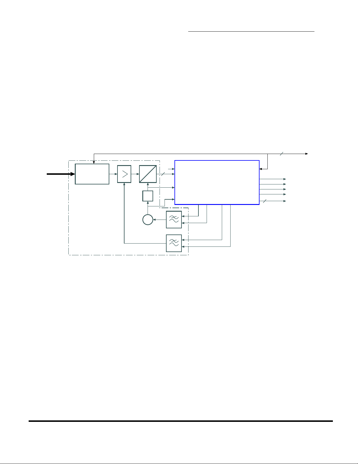
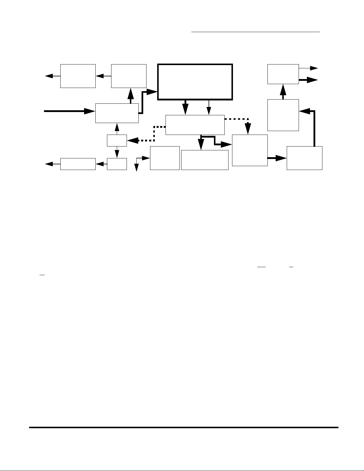
3.2.2 2K-OFDM Demodulator Block
The MC92314 contains also a Demodulator for the Orthogonal Frequency Division Multiplex
transmission scheme according to the 2K-mode of the ETSI specification for digital terrestrial
transmission (see reference [1-1]). Together with the 2K FFT block described in the previous
paragraph it includes all the functions required to demodulate the information transmitted in one
single UHF channel.In Figure 3-3 the blockdiagram of the OFDM block is given, followedby the
description of the functional blocks.
Preliminary Information
Fr
MOTOROLA Single Chip DVB-T Demodulator - Rev. 1.3 (11/30/98)
3-2
For More Information On This Product,
Go to: www.freescale.com
Page 21
Freescale Semiconductor, Inc.
Device Description
nc...
, I
or
CLK Loop
Filter & DAC
Clock
VCXO
From ADC
Received Data
AGC
Time Sync
(Coarse &
Fine)
I/Q Demodulator
& Derotator
AFC
AGCAGC-DAC
Channel Data RAM
I2C & Parallel
Interface
FFT Block
TPS & Frame Synchronisation
Extracted
Pilots
Channel Estimation &
Correction
Data
Formatter
Symbol
Deinterleaving & Demapping
Control
G1, G2
Data
Channel
State
Estimation
Figure 3-3. OFDM Demodulator Part of the MC92314
3.2.2.1 I/Q-Demodulator
In this first stage the complex samples are reconstructed from the (real valued) input stream by
means of a discrete Hilbert transformer. The input stream is fed into the Hilbert transformer and
delayed appropriately to calculate the real and imaginary parts of the signal.
emiconduct
eescale S
Fr
3.2.2.2 Derotator
Carrier frequency offsets resulting from local oscillator offsets in the tuner are removed digitally
by means of a NCO and a phase accumulator, that are controlled by the
Automatic Frequency
Control (AFC). During the acquisition phase (when locking onto a DVB-T transmission) the AFC
circuit sweeps permanently through the available range until the correct frequency offset has
been detected. During the tracking phase the control signal for the phase increment is derived
Preliminary Information
from the pilot carriers in the frequency domain.
3.2.2.3 Time Synchronisation
The Time Synchronisation (separated in the coarse synchronisation valid during the acquisition
phase and the fine synchronisation for tracking purposes) sets the FFT window position for the
real OFDM demodulation and controls the clocking of the whole chip.
In the tracking mode the time synchronisation generates the VCXO control signal using the filter
structure given in Figure 3-4 below. The contribution of the proportional branch and of the
integrator branch can be adjusted separately using the Clock Loop Filter Coefficients (see also
paragraph 4.2.2.1.5).
The gain of the proportional part is set using Bits [7:4] and the gain of the integrator part is
adjusted with Bits [3:0].
Single Chip DVB-T Demodulator - Rev. 1.3 (11/30/98) MOTOROLA
3-3
For More Information On This Product,
Go to: www.freescale.com
Page 22
Device Description
Freescale Semiconductor, Inc.
C_Proportional
nc...
, I
or
emiconduct
eescale S
Fr
VCXO
Figure 3-4. Time Synchronisation of the OFDM Block
3.2.2.4 Channel Estimation
To compensate for the impairments of the terrestrial channel it is essential to estimate the
channeltransfer function. Thisestimationis done usingthe scattered andcontinual pilot carriers.
As the scattered pilots change in subsequent OFDM symbols a
symbols isnecessary to build a complete setof pilot information. This set containsone valid pilot
sampleat every 3rdcarrier position. To obtaina channel estimationvalue so theset ends upwith
an estimation value for each carrier position,
3.2.2.5 Channel Estimation RAM
Thechannel estimationRAM must storethe datacarriers untilthe channelestimation is available
for a given OFDM symbol.
3.2.2.6 Channel Correction
In the channel correction block the estimate of the channel transfer function is used to
compensate the influence of the terrestrial transmission. In principle each data carrier’s value is
multiplied with the inverse of the estimate to approximate the desired flat overall frequency
response to as close as possible.
Preliminary Information
Phase
Detector
Integrator
C_Integrator
LPF
time interpolation over 4 OFDM
frequency interpolation must be performed.
sd-DAC
3.2.2.7 Channel State Estimation
To improve the efficiency of the decoding of the inner convolutional code, information about the
reliabilityof each bitreceived viathe transmissionchannel, is generatedduring thedemodulation
process. So data that were transmitted in subchannels disturbed heavily due to echoes or
interference (resulting in alow SNR in these specific subchannels) are marked less reliable than
those transmitted in nearly undisturbed subchannels. In the channel state estimation this
MOTOROLA Single Chip DVB-T Demodulator - Rev. 1.3 (11/30/98)
3-4
For More Information On This Product,
Go to: www.freescale.com
Page 23

nc...
, I
or
Freescale Semiconductor, Inc.
reliability information is generated for each carrier individually and passed together with the
subcarriers data to the following stage.
3.2.2.8 Inner Deinterleaver
Due to the echoes on the transmission path it is obvious that adjacent subcarriers are disturbed
in a similar way: the used bandwidth of 7.61 MHz corresponds to 1705 active carriers, so the
difference in the channel transfer function from one carrier to the adjacent carrier is limited. In
case of a simple parallel to serial conversion adjacent bits of data would suffer from similar
distortions.In this case theViterbi decoder cannotwork with itsoptimal performance. Insteadthe
best performance is given if the disturbance applied to adjacent data bits is uncorrelated. To
achieve this the data of all the relevant subcarriers are interleaved in the transmitter according
to par. 4.3.4 in reference [1-1]. This interleaving has to be reversed prior to the demodulation.
3.2.2.9 Symbol Demapper and Bit Deinterleaver
The modulated (complex valued) frequency domain samples are demapped into 2, 4 or 6
streams depending on the modulation scheme chosen. Each demodulated data bit is extended
to a 3-bit soft decision value using the reliability information from the Channel State Estimation
to support the following FEC.
Device Description
emiconduct
eescale S
Fr
In par. 4.3.4 in reference [1-1], bit interleaving is also specified in order to disperse bursts of bit
errorsin the receiverafter demappingthe complex datasymbols. Thisbit interleaving isreversed
in the Bit Deinterleaver module.
3.2.2.10 Data Formatter
This is the final stage in the OFDM specific part of the DVB-T frontend. It generates from the up
to 6 bitstreams according to par. 4.3.4 in reference [1-1] the correct datastreams corresponding
to the G1 and G2 data to be fed into the Viterbi decoder.
Although the FEC scheme and the format of the data delivered by the OFDM block is identical
to the satellite system there is a fundamental difference in clocking. In the DVB-S system the
data are delivered continuously to the Viterbi decoder, where as, this cannot be the case in
DVB-T. The internal clocking is uncorrelated to the transmitted data rate. Instead of going the
costly way of synthesizing an extra clock signal for the Viterbi decoder, the demodulated data
areoutput in burst modeat an averagefrequency corresponding tothe transmitted data rate.For
details see the paragraph 4.6 OFDM -> FEC Interface in reference [1-1].
Preliminary Information
Single Chip DVB-T Demodulator - Rev. 1.3 (11/30/98) MOTOROLA
3-5
For More Information On This Product,
Go to: www.freescale.com
Page 24
Device Description
Freescale Semiconductor, Inc.
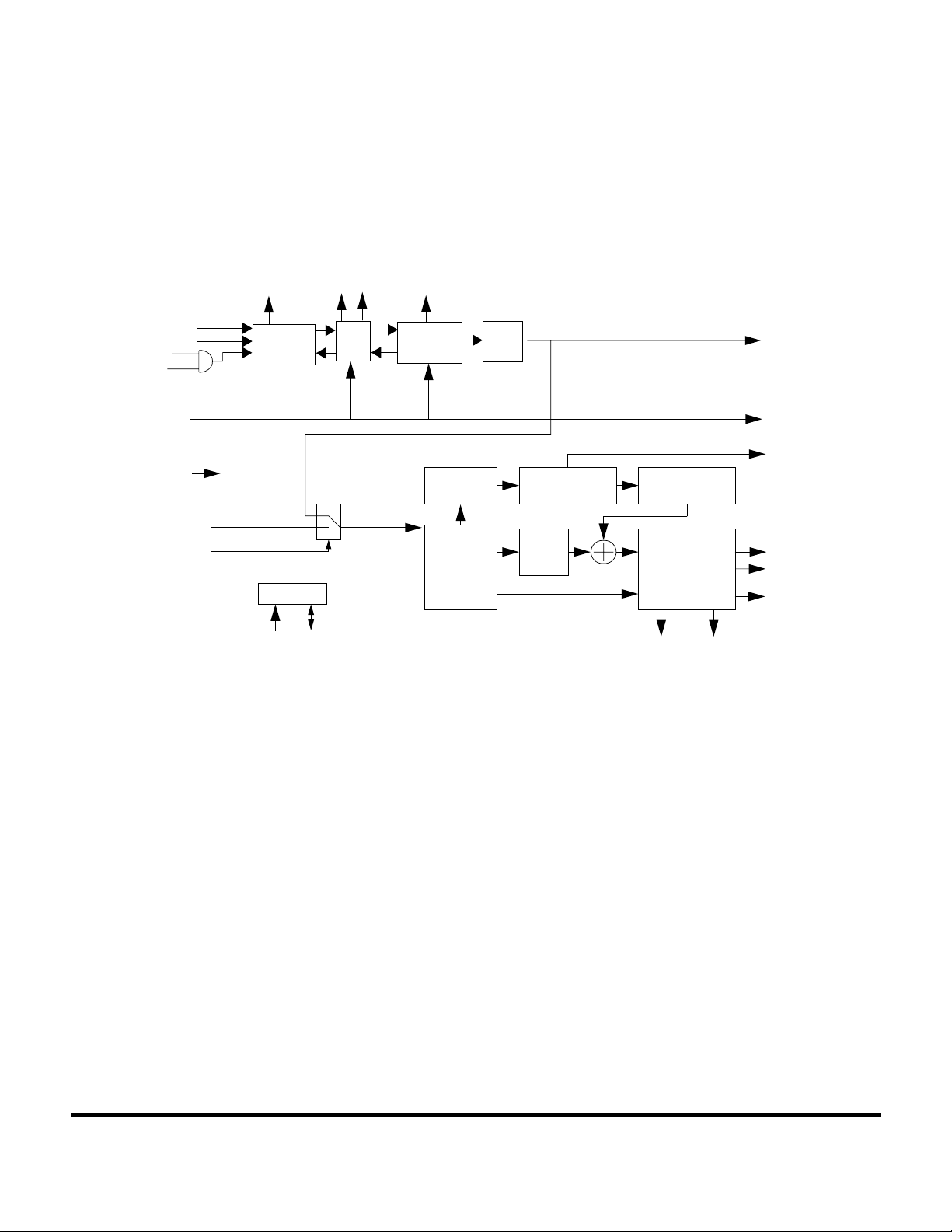
3.2.3 FEC Block
The FEC block completes Motorola’s DVB-T single chip demodulator by providing all the FEC
functions necessary for the reception of DVB-T transmissions. It is fully compliant to the ETSI
specification for digital terrestrial broadcasting (see reference [1-1]).
nc...
, I
or
emiconduct
eescale S
Fr
SR2..0
Depuncturing
CheckByte
Generation
Deinterleav-
er Memory
andAddress
Sequencer
Frame
Synchroniser
Viterbi
Core
Error Detec-
tion and Evalu-
Code-
word
Delay
FIFO
Error Location
and Value Gener-
Descrambler for
Energy Dispersal
Removal
Frame Detection
INSYNC
FSTART
VO
BITCLKOUT
RERRU
SPO7..0
DOVALID
SVALO
G1DATA2..0
G2DATA2..0
VDCLK
DIVALID
SYMCLK
RESB
SERIALIN
RSONLY
VLCK
Node
Synchroniser
I2C Interface
VEF
VFF
FIFO
SDASCL
Figure 3-5. Block Diagram of the FEC Block
3.2.3.1 Node Synchroniser
3.2.3.1.1 Syndrome Based Node Synchronisation
Priorto producing validdata the Viterbidecoder block mustsynchronise to theinput data stream,
Preliminary Information
including removing any phase ambiguity in the received symbols and determine the punctured
code rate transmitted.
The Viterbi block employs a method known as Syndrome Based Node Synchronisation to
achieve both I & Q symbol and punctured rate Synchronisation. This method has certain
advantages over other more common Synchronisation methods such as observation of path
metric growth rates and re-encoding of the received data stream:
• Path metric growth observations are relatively sensitive to input magnitude variations and
require multiple estimation cycles to detect Synchronisation.
• Re-encodingof the datastream (usinga convolutional encoder)requires multipleestimation
cycles and can increase the latency of the decoder.
MOTOROLA Single Chip DVB-T Demodulator - Rev. 1.3 (11/30/98)
3-6
For More Information On This Product,
Go to: www.freescale.com
Page 25

nc...
, I
or
Freescale Semiconductor, Inc.
Syndrome based node synchronisation is independent of the average input magnitude and can
also easily detect changes of the synchronisation state.
The theory is based on the observation that the product of the incoming data and a syndrome
(predetermined by simulation for each data rate) is zero if synchronised correctly. In any other
case, the probability of 0’s vs. 1’s in the product increases. In the extreme case, i.e. the node
synchronisation is completely wrong, the product is random and there is equiprobability of 0’s
and 1’s. This behaviour is exploited for syndrome based node synchronisation.
3.2.3.1.2 Synchronisation States
The possible states that the synchroniser has to deal with are a combination of the following
factors:
• The phasing of the received symbols. The synchroniser must decide which of two possible
states theI and Q inputstreams are in. Theycan either be processedas-is or can berotated
o
to account for constellation rotation in the receiver.
90
• Determination of the framing of the I and Q bit streams so as to extract the correct symbol.
There are four possible ways to frame the two bit streams and the synchroniser must
determine the correct one.
Device Description
emiconduct
eescale S
Fr
3.2.3.1.3 Synchroniser Parameters
The synchroniser is based on an estimator which determines whether the received symbol
sequence is in the correct synchronisation state. This estimate is based on single sided
sequential probability ratio tests (SPRTs). The tests are based on the accumulation of the loglikelihood ratio (LLR) that a certain hypothesis (in-sync or out-of-sync) for the input sequence
holds. A vote for a hypothesis is obtained if the accumulated LLR reaches a certain threshold.
The accumulator value L is computed as shown in the flowchart in Figure .
NOTE
If a vote for out-of-sync occurs, the synchronisation state (which is
Preliminary Information
2
I
output at
hypothesis.
C register SYNCH_STATE) is increased to test the next
Single Chip DVB-T Demodulator - Rev. 1.3 (11/30/98) MOTOROLA
3-7
For More Information On This Product,
Go to: www.freescale.com
Page 26
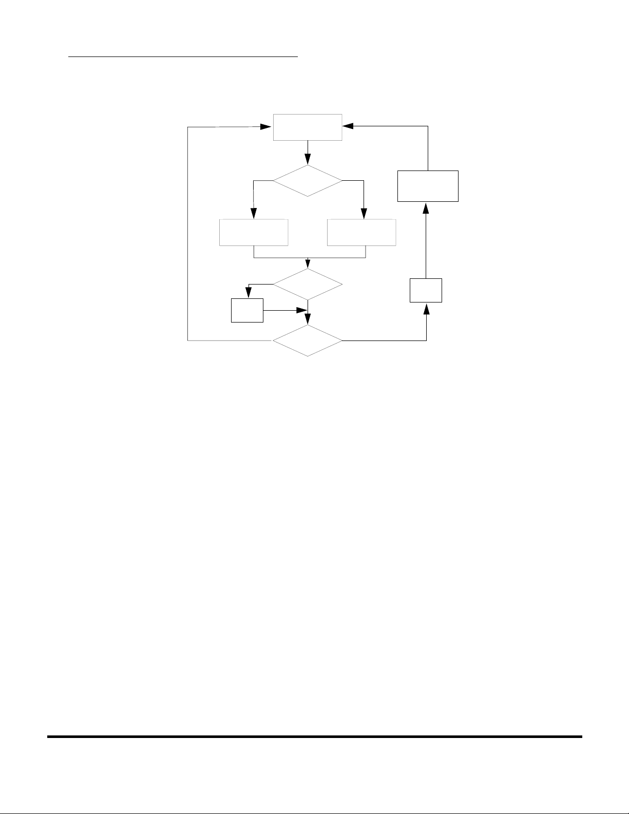
Device Description
Freescale Semiconductor, Inc.
Read Syndrome
Bit
nc...
, I
or
emiconduct
eescale S
Fr
IN-SYNCH
Y
L = L + INC
Y
L = 0
N
Bit == 1
L < 0
N
L>=THRESH
N
L = L - DEC
Y
Move To
Next State
L = 0
OUT-OF-SYNCH
Figure 3-6. Synchronisation Flow
3.2.3.1.4 Choice of DEC and THRES
The constants INC, DEC and THRES influence the acquisition behaviour of the synchroniser as
well asit’s robustness. Theconstants INC and DECshould be chosen suchthat the accumulator
is driven towards zero in the case that the syndrome sequence is identifying the in-sync state
(i.e. rate of zeroes is p
Ifthe syndromesequence isidentifying an out-of-syncstate (i.e.p
).
0
=0.5) theaccumulator should
0
be driven with approximately equal average increments towards the threshold. Obviously, the
synchroniser will erroneously vote for out-of-sync condition if the channel SNR falls below a
certain limit since p
Preliminary Information
will approach 0.5 for very low SNR.
0
• The decoder uses a fixed Increment of INC = 32.
• DEC is set via I
2
C register DEC[4:0] and can have a maximum value of 32, default selection
of DEC values according to the rate being decoded is enabled by setting the DDEC bit in
the CONFIG register to 0. The default values of DEC for each of the supported rates is
shown in Table 3-1.
2
I
• THRES is set via
C register THRESHOLD and can have a maximum value of 32, default
selection of THRES = 8 is enabled by setting the DTHRES bit in the CONFIG register to be
0.
9
The actual value of THRES is interpreted as <register_value> x 2
.
MOTOROLA Single Chip DVB-T Demodulator - Rev. 1.3 (11/30/98)
3-8
For More Information On This Product,
Go to: www.freescale.com
Page 27

Freescale Semiconductor, Inc.
Device Description
The defaults have been chosen such that the synchroniser will operate correctly (but with a
performance degradation) roughly 2 dB below the output error rate, which is required for quasi
-4
error free operation (BER of the decoded stream approximately =2 x 10
).
Table 3-1. Default Settings For DEC Parameter
nc...
, I
or
emiconduct
eescale S
Lower SNR
Rate Dec
1/2 29 1.2 3.0 2.15 0.100
2/3 26 2.0 3.5 2.49 0.062
3/4 25 2.4 4.0 3.00 0.042
5/6 24 2.9 4.5 3.51 0.026
7/8 23 3.5 5.2 4.10 0.017
Boundary
(dB)
Quasi
Error
Free SNR
(dB)
Design
Point SNR
(dB)
Design
Point
Channel
BER
3.2.3.1.5 Synchroniser Performance
The performance of the synchroniser can be characterized by three figures:
Short Average Run Length (SARL):
•
Thisis the meantime requiredto detect thatthe currentlyinvestigated synchronisation state
is not the correct synchronisation state.
The SARL is calculated as:
SARL
2XTHRES
-----------------------------=
INC DEC–
NOTES
Preliminary Information
SARL performance is not affected by the channel SNR since the
syndrome sequence is composed of equiprobable 1’s and 0’s for an
out of synch condition and low channel SNR would also result in
equiprobable 1’s and 0’s.
Fr
Reacquisition Average Run Length (RARL):
•
This is the mean time between a erroneous detection of a change of the synchronisation
state and successful acquisition of the new synchronisation state (reacquisition).
The RARL is calculated as:
SARL
RARL
Single Chip DVB-T Demodulator - Rev. 1.3 (11/30/98) MOTOROLA
---------------------------------------- -=
syncstates 1–()
For More Information On This Product,
Go to: www.freescale.com
3-9
Page 28

nc...
, I
or
Device Description
Where “syncstates” is given by:
Table 3-2. Number of Syncstates in Code Rates
For automatic rate selection the synchroniser investigates the
possible synchronisation states one after the other and RARL is
calculated as follows:
Freescale Semiconductor, Inc.
Rate Synchstates
1/2 2
2/3 6
3/4 4
5/6 6
7/8 8
NOTE
7
-- -
8
RARL Synchstates
∑
1
rate
-- -=
2
SARL×=
emiconduct
eescale S
Fr
Long Average Run Length (LARL): This is the mean time until the algorithm incorrectly
•
indicates a change of the synchronisation state that did not actually occur.
This grows exponentially with the threshold value THRES.
NOTE
While the SARL and RARL can be determined analytically the
evaluation of the LARL is nontrivial and is best determined via
simulation.
Figure 6-2. showsthe simulated LARL for all code rates,the channel error rate is set sothe SNR
Preliminary Information
is 1dB below the error rate required for QEF operation at the output of Viterbi decoder.
MOTOROLA Single Chip DVB-T Demodulator - Rev. 1.3 (11/30/98)
3-10
For More Information On This Product,
Go to: www.freescale.com
Page 29

LARL (Syndrome Bits)
2
1e+05
5
2
Freescale Semiconductor, Inc.
+
♦
•
◊
♥
#
Device Description
•
r=1/2, design point
•
+
r=1/2, quasi error free
×
r=1/2, worst case
♦
r=2/3, design point
♥
r=3/4, design point
#
r=5/6, design point
◊
r=7/8, design point
nc...
, I
or
emiconduct
eescale S
Fr
1e+04
1e+03
+
♦
5
•
2
◊
♥
#
+
♦
××
•
×
×
××
THIS GRAPH NEEDS TO BE EXTENDED!
THE SCALES TO SHOW THE THRESHOLD UP TO 5000
AND THE CURVES EXTRAPOLATED
5
•
×
2
0.50 1.00 1.50 2.00 2.50
Preliminary Information
THRES x 10
3
Figure 3-7. LARL Versus THRES At Various Design Points
For rate1/2 (worst case for the synchroniser) the results for QEF (BER = 0.0789) and 2.8 dB
below (BER = 0.125) are shown extrapolated.
From it can be seen that the LARL increases with decreasing SNR. For QEF operation a
1
threshold below5000 is sufficientto obtain less thanone synchroniser error perday for a rate
/2.
3.2.3.1.6 Lock Detection and Time-out
Lockof the decoderis indicatedif the stateof thesynchroniser has notchanged fora significantly
long time, this period is measured in number of syndrome bits. The time-out period can be set
2
via the I
set to 0. The actual period is TIMEOUT * 2
Single Chip DVB-T Demodulator - Rev. 1.3 (11/30/98) MOTOROLA
C register TIMEOUT, a default value of 8 is used if bit DLT in the CONFIG register is
11
syndrome bits.
3-11
For More Information On This Product,
Go to: www.freescale.com
Page 30

Freescale Semiconductor, Inc.
Device Description
• If the accumulator value L does not reach the threshold value THRES within the period
specified by TIMEOUT then it is reset and the decoder continues to indicate a locked state.
• If L exceeds THRES before the end of the TIMEOUT period then an out of lock condition is
declared and the synchroniser moves to the next state and restarts the synchronisation
process.
To avoid false lock indications, and to quickly detect out of lock situations the optimal value for
TIMEOUT is SARL * 4.
3.2.3.2 Viterbi Error Correction
3.2.3.2.1 BER vs. SNR Performance
Figure 3-8 shows the performance curves for each code rate as a function of Bit Error Rate
(BER) versus channel Signal to Noise Ratio (SNR). The graph also shows the Quasi Error Free
(QEF) operating limit at 2 * 10
nc...
an AWGN channel with a normalized gain of 1 at the output of the receiver A/D.
-4
. The graph was generated assuming QPSK transmission over
, I
or
emiconduct
eescale S
Fr
In paragraph 5.3.2.3 an example is given how to obtain a BER estimate from the QVAL values
that are available from the FEC register.
Preliminary Information
MOTOROLA Single Chip DVB-T Demodulator - Rev. 1.3 (11/30/98)
3-12
For More Information On This Product,
Go to: www.freescale.com
Page 31

nc...
, I
or
QEF
BER
1e-01
1e-02
1e-03
1e-04
Freescale Semiconductor, Inc.
2
5
2
5
2
5
2
+
•
•
Device Description
•
r=1/2
+
r=2/3
×
r=3/4
♥
×
♦
+
×
+
•
•
♥
♦
♥
♦
×
+
×
+
•
•
•
♥
♦
♥
♦
×
♦
♥
×
+
•
+
×
♥
♥
♦
♥
♥
♦
r=5/6
♥
r=7/8
♥
emiconduct
eescale S
Fr
5
2
0.00 1.00 2.00 3.00 4.00 5.00 6.00
Preliminary Information
Figure 3-8. BER versus SNR
•
+
♦
×
Eb/N0 (dB)
3.2.3.2.2 Decoding Latency
A survivor depth of 96 is used to ensure reliable error correction for highrate punctured codes
such as the7/8 code. The latency of the decoder(in symbols) is approximately 2.5 x thesurvivor
depth (the uncertainty in the latency is due to the input FIFO which gives a range of + or - 16
symbols).
NOTE
This latency applies for all coding rates not just the 7/8 rate.
The absolute worst case latency is thus: (2.5 x 96) + 16 = 256 symbols.
Single Chip DVB-T Demodulator - Rev. 1.3 (11/30/98) MOTOROLA
3-13
For More Information On This Product,
Go to: www.freescale.com
Page 32

Freescale Semiconductor, Inc.
Device Description
3.2.3.2.3 Generator Polynomials
The Viterbi decoder is designed to decode bit streams encoded using the DVB standard
generator polynomials (171
, 1338) as shown in Figure 3-9.
8
171
8
+
nc...
, I
or
emiconduct
eescale S
Fr
Data In
Data Out
+
133
8
Figure 3-9. Generator Polynomials
3.2.3.2.4 Punctured Codes
The Viterbi decoder is able to decode a basic rate 1/2 convolutional code and the “standard”
punctured codes for a k=7 constraint length. The punctured maps are shown in the table below.
Specific bits of the original rate 1/2 code sequence are periodically deleted prior to transmission
according to the entries in the table, where a 0 means that the bit is deleted and a 1 means that
the bit is transmitted.
Table 3-3. Deletion Map For Punctured Rate 1/2 Codes
Coding Rate Puncture Map
1/2
Preliminary Information
2/3
3/4
5/6
7/8
1
1
11
10
110
101
11010
10101
1111010
1000101
3.2.3.2.5 Rate Encoding Data Word
The code rate actually being decoded by the decoder is indicated via external pins SR2..SR0
and via the I
MOTOROLA Single Chip DVB-T Demodulator - Rev. 1.3 (11/30/98)
3-14
2
C interface.
For More Information On This Product,
Go to: www.freescale.com
Page 33

Freescale Semiconductor, Inc.
Device Description
Table 3-4 shows the encoding of the rate information into a three bit word. This information is
used for output information when using automatic synchronisation or for control information
2
when the block is being externally controlled via the I
C interface.
Table 3-4. Rate Encoding
nc...
, I
or
emiconduct
eescale S
Fr
Coding Rate
1/2 000
2/3 001
3/4 010
5/6 011
7/8 100
Automatic 111
Notes:
Automatic rate selection is only used as an input value
when internal synchronisation is used. The decoder will
never output 111 as a coding rate.
All other states of the 3 bit data word are unused.
Data Word
This table is referred to throughout this document when discussing the various rates supported
by the decoder.
3.2.3.2.6 Input Data Format
TheI and Qdata inputto the decodercan beinterpreted as eithersign-magnitude oroffset binary
format. The choice of input format is specified by setting the IFSbitin the CONFIG register bank
of the I2C interface. The default after RESET_N is to use offset binary.
Table 3-5. I And Q Input Format
VC0[2:0]/VC1[2:0]
Interpretation
Preliminary Information
strong 0
.
.
weak 0
weak 1
.
.
strong 1
IFS = 0
(offset binary)
000 011 100
001 010 101
010 001 110
011 000 111
100 100 000
101 101 001
110 110 010
111 111 011
IFS = 1
(sign-magnitude)
2’s complement
(internal format)
3.2.3.2.7 Channel SNR Measurement
The synchroniser generated syndrome sequence (p
value. The average value of the number of 1’s accumulated from p
2
period and is accessible via the I
Single Chip DVB-T Demodulator - Rev. 1.3 (11/30/98) MOTOROLA
C interface.
) is used to determine the channel SNR
0
is calculated over a known
0
3-15
For More Information On This Product,
Go to: www.freescale.com
Page 34

Device Description
Freescale Semiconductor, Inc.
nc...
, I
or
The window length used is specified by the AVRG_PERIOD register and is interpreted as
AVRG_PERIOD[3:0] * 2
register bank is set to 1. The number of 1’s in the syndrome stream (divided by 16) which are
accumulated over the specified period may be read from the registers QVALMSB[7:0] and
QVALLSB[7:0].
The estimated value of p
The value of p
curves shownin Figure 3-10.This signal quality value correspondsto the channel SNRofQPSK
transmission over an AWGN channel. The curves are generated specifically for the syndrome
polynomials actually used in the decoder. To derive a channel SNR value simply look up the
value on the x-axis of a given p
can be directly related to the signal quality for the various code rates via the
0
15
, the default period of 8 * 215 is used if the DAP bit in the CONFIG
is:
0
p
0
value for a given code rate.
0
QVAL 2
1
-------------------------------------–=
PERIOD 2
4
×
15
×
emiconduct
eescale S
Fr
Preliminary Information
MOTOROLA Single Chip DVB-T Demodulator - Rev. 1.3 (11/30/98)
3-16
For More Information On This Product,
Go to: www.freescale.com
Page 35

Freescale Semiconductor, Inc.
Device Description
nc...
, I
or
emiconduct
p0 x 10
900.00
850.00
800.00
750.00
700.00
650.00
600.00
550.00
500.00
-3
×
+
♦
×
♥
+
♦
×
+
♥
♦
×
+
♥
♦
+
×
♥
♦
+
×
+
♥
×
♦
+
×
•
♦
♥
+
•
×
♦
+
♥
•
×
+
♦
•
♥
×
+
•
♦
×
♥
•
+
♦
•
×
+
+
×
+
×
•
+
×
•
+
+
•
•
•
•
♦
•
×
♦
•
♥
•
♦
•
♥
♦
♥
♥
•
•
•
•
Preliminary Information
0.00 2.00 4.00 6.00
+
♦
×
♥
+
×
♦
♥
+
×
♦
+
♥
×
♦
+
♥
•
•
•
•
•
•
•
r=1/2
+
r=2/3
×
r=3/4
♦
r=5/6
♥
r=7/8
Eb/N
0
eescale S
Fr
3.2.3.2.8 Accuracy of SNR Estimate
The accuracy of the p
0
Figure 3-10. p0 Versus Channel SNR
estimate of channel SNR increases with longer averaging periods and
with increased SNR. Table 3-6 shows the effect of increasing the AVRG_PERIOD for different
Single Chip DVB-T Demodulator - Rev. 1.3 (11/30/98) MOTOROLA
For More Information On This Product,
Go to: www.freescale.com
3-17
Page 36

Freescale Semiconductor, Inc.
Device Description
code rates and channel SNR. It shows the probability that the estimate from the graph is within
+/- 0.1 dB of the actual channel SNR.
nc...
, I
or
emiconduct
eescale S
Fr
Table 3-6. Probability Of p
AVRG_PERIOD
1 32768 0.541559 0.999799
2 65536 0.700163 1
4 131072 0.855141 1
8 (default) 262144 0.960214 1
15 491520 0.995069 1
Fromthe tableit can beseen thateven usingthe defaultvalue forAVRG_PERIOD the probability
that the p
AVRG_PERIOD values or increased SNR values the probability is 100% for all practical
purposes.
3.2.3.3 Frame Synchronisation
3.2.3.3.1 MPEG Frame Synchroniser and Deinterleaver
This section of the manual describes the Frontend of the Reed-Solomon decoder in the
MC92314. The data received from the Viterbi decoder is internally a continuous stream of bits
and must be segmented into blocks (MPEG-2 Transport Packets) and subsequently into bytes
that the Reed-Solomon can manipulate. The Frame Synchroniser recognizes the
Synchronisation Bytes (Sync Bytes) embedded in the data stream and communicates these as
frame boundaries to the Reed-Solomon decoder and the other functional blocks. The 12x17
Forney Deinterleaver processes the input bit stream to break up and distribute the longer burst
errors throughout the MPEG-2 packet.
3.2.3.3.2 Frame Structure and Synchronisation Scheme
The MPEG-2 Transport Packet consists of one leading Sync Byte (0x47), 187 information bytes
and 16Reed-Solomon Check Bytes (for atotal of 204). Inaddition, the Sync Byte ofevery eighth
packet is inverted from 0x47 to 0xB8. The frame structure of the interleaved data is depicted in
Figure 3-11. The synchroniser uses thisstructure to determine the byte andframe boundaries to
synchronise the deinterleaver and the decoder and also to resolve the
within the input stream.
estimate of SNR is within 0.1 dB is 96% (even for small SNR values). For increased
0
Preliminary Information
# Of Samples
Probability Of +/- 0.1dB Accuracy
r=1/2, E
Accuracy
0
=1.2 r=7/8, Eb/N0=3.5
b/N0
π-ambiguity of the data
MOTOROLA Single Chip DVB-T Demodulator - Rev. 1.3 (11/30/98)
3-18
For More Information On This Product,
Go to: www.freescale.com
Page 37

Freescale Semiconductor, Inc.
Device Description
nc...
, I
or
emiconduct
SYNC
(1 BYTE)
DATA
(187BYTES
RS REMAINDER
(16 BYTES)
)
Pseudo Random Binary Sequence Period
(1504 BYTES)
SYNC
(1 BYTE)
DATA
(187BYTES)
RS REMAINDER
(16 BYTES)
SYNC
(1 BYTE)
Figure 3-11. MPEG-2 Frame Structure
3.2.3.3.3 Frame Synchroniser Modes
The Frame Synchroniser has two operation modes: the Acquisition and Tracking Modes. The
Acquisition Mode starts when an initial Sync Byte is detected and continues until a specified
number of additional Sync Bytes has been found at the correct positions within a specified
number of MPEG-2 transport packets. In this case the Tracking Mode is entered. The Frame
Synchroniser remains in the Tracking mode as long as the (different) set of synchronisation
2
conditions for tracking is met and maintained. Four integer parameters (set through the I
C
Interface) are used to establish these two modes: Aq_Sync_Thresh, Aq_Ref_Thresh,
Tr_Sync_Thresh andTr_Ref_Thresh. Aq_Sync_Thresh and Aq_Ref_Thresh areusedto set the
desired level of Acquisition conditions. If Aq_Sync_Thresh Sync Byte or inverted Sync Byte
matches are found in Aq_Ref_Thresh frame spaced positions (e.g. Aq_Sync_Thresh = 2 and
Aq_Ref_Thresh = 8: if 2 Sync Bytes are found in 8 MPEG-2 frames or in 8 x 204 = 1632 bytes),
In_Syncis signalled and theTracking Mode isenabled. Otherwise, thecorrelation upon theinput
bit stream is continued and the Frame Synchroniser further remains out of the synchronisation
state. In the Tracking Mode, Tr_Sync_Thresh Sync Byte or inverted Sync Byte matches are
necessary in Tr_Ref_Thresh frame spaced positions in order to stay In_Sync. See Figure 3-12
for the state diagram of the Frame Synchroniser.
The parameters Aq_Ref_Thresh (default: 8) and Tr_Ref_Thresh (default: 31) can be set
between 0 and 31 and the parameters Aq_Sync_Thresh (default: 2) and Tr_Sync_Thresh
Preliminary Information
(default: 3) can be set between 0 and 7.
eescale S
Fr
Single Chip DVB-T Demodulator - Rev. 1.3 (11/30/98) MOTOROLA
For More Information On This Product,
Go to: www.freescale.com
3-19
Page 38

Device Description
Freescale Semiconductor, Inc.
Search for 0x47 and
0xB8 in the MPEG-2
Transport Stream
First Match
_1_1_1
Out of
Sync
# of Sync Bytes found is less than
Aq_Sync_Thresh occurrences in
Aq_Ref_Thresh MPEG-2 frames
# of Sync Bytes found is less than
Tr_Sync_Thresh occurrences in
Tr_Ref_Thresh MPEG-2 frames
nc...
, I
or
emiconduct
eescale S
Fr
Correlate at 204 byte
spaced positions
Acquisition
Mode
Correlate at 204 byte
spaced positions
# of Sync Bytes found is equal or
more than Aq_Sync_Thresh occurrences in Aq_Ref_Thresh MPEG-2
frames
Tracking
Mode
# of Sync Bytes found is equal or
more than Tr_Sync_Thresh occurrences in Tr_Ref_Thresh MPEG-2
frames
Figure 3-12. Frame Synchroniser State Diagram
3.2.3.3.4 π-Ambiguity Resolution
While in the Tracking Mode,
π-ambiguity is also determined and resolved. As frames enter the
Frame Synchroniser the number of Sync Bytes found at frame start positions are compared to
the number of inverted Sync Bytes that have been identified. If three inverted Sync Bytes are
found per Sync Byte occurrence, a
Demodulator is assumed and all received bits are inverted to correct the
π-offset synchronisation of the Viterbi decoder or QAM
π phase mismatch at
the output.
3.2.3.3.5 Frame Synchroniser Performance
The False Lock Probability (going into or staying in a state of synchronisation although
Preliminary Information
synchronisation is lost), Loss of Sync Probability (detecting an Out_of_Sync state in spite of
being In_Sync), Acquisition Time (time needed to assert the In_Sync condition), and Loss of
Sync Time (time required to detect an Out_of_Sync situation when synchronisation is lost) are
primarily influenced by the parameters: Aq_Ref_Thresh, Aq_Sync_Thresh, Tr_Ref_Thresh and
Tr_Sync_Thresh, and the BER out of the Viterbi decoder. Typically, in the 1632 bit (204 x 8 =
1632 bits) frame, there are an average of 12.75, including 11.75 coincidental, matches of the
(inverted)Sync Byte.Assuming thesematches are uniformlydistributed inthe frame,the number
of synchronisation trials (going from the Out_of_Sync state into the Acquisition Mode, see
Figure 3-12) until the correct position of the Sync Byte is found averages 12.75 times. The
probability of not going In_Sync can be seen in Figure 3-13 for a BER of 5E-2 and in Figure 3-
-4
14 for a BER of 1 * 10
. The value “n” represents the parameter Aq_Sync_Thresh and on the x-
axis is Aq_Ref_Thresh. These figures also show the Loss of Sync Probability if the Frame
MOTOROLA Single Chip DVB-T Demodulator - Rev. 1.3 (11/30/98)
3-20
For More Information On This Product,
Go to: www.freescale.com
Page 39

Freescale Semiconductor, Inc.
Synchroniser isin the Tracking Mode(the value “n” now correspondsto Tr_Sync_Thresh and on
the x-axis is Tr_Ref_Thresh).
The AcquisitionTime increases with highervalues of Aq_Ref_Thresh and decreaseswith higher
MPEG-2 Transport Stream input data rates. Each of the 12.75 synchronisation trials needs the
duration of Aq_Ref_Thresh (default: 8) times 204 bytes, times 8 bits/byte, and divided by the
input data bit rate. At 50 Mbit/s, the time interval until the correct position of the Sync Byte is
found averages 3.3 ms at a BER of 5 * 10
0.1
-2
Device Description
.
nc...
, I
or
emiconduct
eescale S
Fr
0.001
1E-05
n=7
1E-07
Probability
1E-09
1E-11
Preliminary Information
1E-13
n=1
1E-15
0
10
Number of Frames
20
30
Figure 3-13. Loss of Synchronisation Probability for BER=5E-2
Single Chip DVB-T Demodulator - Rev. 1.3 (11/30/98) MOTOROLA
3-21
For More Information On This Product,
Go to: www.freescale.com
Page 40

Device Description
Freescale Semiconductor, Inc.
1E-10
1E-20
1E-30
1E-40
nc...
, I
1E-50
or
emiconduct
eescale S
Fr
1E-60
Probability
1E-70
1E-80
1E-90
1E-100
Preliminary Information
Figure 3-14. Loss of Synchronisation for BER=1E-4
The False Lock Probability is independent of the BER and is depicted in Figure 3-15 for both the
Acquisition and Tracking Modes. It gives the probability that in a random data stream the
specified number of sync byte values (given with the .._Sync_Thres value) in the expected
distance of 204 bytes occurs in the specified window of .._Ref_Thresh packets.
0
15
Number of Frames
n=7
n=1
30
Note that whenever a pattern with a period of 1632 bytes is fed into the scrambler at the
transmitter side, a bit patternthataccidentally matches the Sync Byte has a 1632 period as well.
This applies to any 1632 byte periodical pattern.
MOTOROLA Single Chip DVB-T Demodulator - Rev. 1.3 (11/30/98)
3-22
For More Information On This Product,
Go to: www.freescale.com
Page 41

Freescale Semiconductor, Inc.
EXAMPLE: Considering, for example, the case that an all zero bit stream is fed into the
scrambling block at the transmitter. The Frame Synchroniser may lock falsely onto this bit
pattern, if parameters Aq(Tr)_Ref_Thresh are set to eight times Aq(Tr)_Sync_Thresh or more
(see “m=8n” line in Figure 3-15).
.
0.1
0.001
Device Description
n=1
nc...
, I
or
emiconduct
eescale S
Fr
1E-05
1E-07
1E-09
Probability
1E-11
1E-13
Preliminary Information
1E-15
0102030
Number of Frames
Figure 3-15. False Lock Probability
n=7
m=8n
3.2.3.4 Deinterleaver
3.2.3.4.1 Deinterleaver Functionality
The error protected packetsof 204 bytes are interleaved in the transmitter and the Deinterleaver
must process the byte stream before the Reed-Solomon decoder. The Deinterleaver is a
Convolutional Forney Deinterleaver with I=12 branches. Each branch consists of a shift register
with M(11-j) cells (M=17, j=branch index). Each register has a word length of eight bits so that
Single Chip DVB-T Demodulator - Rev. 1.3 (11/30/98) MOTOROLA
3-23
For More Information On This Product,
Go to: www.freescale.com
Page 42

Freescale Semiconductor, Inc.
Device Description
the data stream is deinterleaved byte wise. For synchronisation purposes, the (inverted) Sync
Bytes (as well as some 16 other bytes) are always routed in the “0” branch of the Deinterleaver.
Figure 3-16 depicts a conceptual diagram of the Convolutional Forney Deinterleaver.
nc...
, I
or
emiconduct
j=0
8
8 bits
3.2.3.4.2 Deinterleaver Latency
The latency of the12x17 Forney Deinterleaver is 17963 CLOCK cycles (not including the Frame
Synchroniser synchronisation acquisition time).
3.2.3.5 Reed-Solomon Decoder
3.2.3.5.1 Reed-Solomon Decoder Module
The algorithmic parameters of the Reed-Solomon decoder used in this block were chosen
according to the DVB Specifications. The arithmetic isperformed using a Finite Field GF(256) of
byte data which is specified by the Field Generator Polynomial:
9
10
11
Figure 3-16. Deinterleaver Principle Block Diagram
11 X 17
3 X17
8 bits
2 X 17 Bytes
17
p(x) = x8 + x4 + x3 + x2 +1
Preliminary Information
The Reed-Solomon decoder works on a shortened (204,188,8) code with Generator Polynomial
eescale S
Fr
g(x) = (x+α
composed of188 information bytes followed by 16parity check bytes. Using thiscode,the ReedSolomon decoder is able to detect and correct up to 8 byte errors per Codeword (a byte error
specifies an erroneous byte, independently of the number of corrupted bits), which can be
arbitrarily distributed within the data and check locations in a Codeword.
The following is a summary of the Reed-Solomon parameters:
• R = 16 Check Bytes
• d = 8 Detection Power
• K = 188 Message Length
• m = 8 Symbol Size in Bits
MOTOROLA Single Chip DVB-T Demodulator - Rev. 1.3 (11/30/98)
3-24
0
)(x+α1)...(x+α15), where α=0x02. One Codeword consists of a total of 204 bytes,
For More Information On This Product,
Go to: www.freescale.com
Page 43

Freescale Semiconductor, Inc.
• N = 204 Codeword Length
• T = 8 Number of Error Corrections
3.2.3.5.2 Reed-Solomon Functional Description
The architecture of the Reed-Solomon decoder is shown in Figure 3-17. The Re-Encoder
consists of a Linear Feedback Shift Register (LFSR) of length 16 (bytes) with the feedback
connections as specified by the Code Generator Polynomial Coefficients. For each Codeword
arriving byte by byte, the Re-Encoder performs a division of this Codeword by the Code
Generator Polynomialand stores the remainder.After processing the first 188information bytes,
the Encoder appends the resulting 16 remainder bytes to the byte stream. If, after processing
188 bytes, the Re-Encoder register contents are identical to the 16 last bytes of the Codeword,
the Codeword is assumed to have been received without error. Otherwise, the Syndrome (the
EXOR of the 16 parity check bytes) and the register contents are stored in the Syndrome RAM.
Device Description
nc...
, I
or
emiconduct
eescale S
Fr
From the Syndrome, the Reed-Solomon Core iteratively determines the Error Location
Polynomial (ELP) and the Error Evaluation Polynomial (EEP). The roots of the ELP specify the
errorlocations inside theCodeword. These rootsare determined inthe Chien SearchUnit, which
checks for roots by evaluating the ELP for all 255 possible field elements. Simultaneously, the
EEP polynomial is evaluated. For each root found, the corresponding EEP value is used to
correct the byte error at the specific bit locations. The input data is stored in the Codeword RAM
(Reed-Solomon FIFO) during the operation of the Core and the Chien Search Unit in order to
take account of the latencies therein. After the roots and error values are determined by the
Chien Search Unit, the data is read from the FIFO, and the necessary byte corrections are
performed in the Error Correction Unit.
If more than8 byte errors occur in a singleframe, this is recognized by the decoderand the input
data is output unchanged. In this case, the “transport_error_indicator” bit in the MPEG-2
Transport Header is set and the RERRU output shall be asserted.
Preliminary Information
Reed-Solomon
Re-Encoder LFSR
Syndrome
Word RAM
Error Location
and Error
Evaluation
Error Location
and Error
Correction
Reed-Solomon
Codeword FIFO
Figure 3-17. Reed-Solomon Block Diagram
Single Chip DVB-T Demodulator - Rev. 1.3 (11/30/98) MOTOROLA
3-25
For More Information On This Product,
Go to: www.freescale.com
Page 44

Freescale Semiconductor, Inc.
Device Description
3.2.3.5.3 Reed-Solomon Performance Analysis
The performance was evaluated by applying BPSK Modulation to the input bits and transmitting
over an Additive White Gaussian Noise (AWGN) channel at different Signal-to-Noise Ratios
(SNR). The results are shown in Figure 3-18. For high input byte error rates the Reed-Solomon
is not able to correct errors since there are too many errors per frame. After crossing the point
wherethe average input byteerror rate becomeslower than 8/204,the error correctioncapability
of the (204,188,8) code is used to correct most of the errors, leading to a substantial decrease
in byte error rate.
nc...
, I
or
emiconduct
eescale S
Fr
Preliminary Information
Figure 3-18. Input Byte Error Rate versus Output Byte Error Rate
MOTOROLA Single Chip DVB-T Demodulator - Rev. 1.3 (11/30/98)
3-26
For More Information On This Product,
Go to: www.freescale.com
Page 45

Freescale Semiconductor, Inc.
3.2.3.5.4 Reed-Solomon Bit Error and Bad Frame Monitor
There are two parameters accessible through the I
circuit uses to track error rates: BER_COUNT and BAD_FRAME.
BAD_FRAME
2
C Interface that the Reed-Solomon decoder
Device Description
nc...
, I
or
emiconduct
eescale S
Fr
This parameter gives the number of bad frames that could not be decoded and corrected during
an intervalof frames specified throughTIME_COUNT (another I
BER_COUNT
BER_COUNT is the number of bit errors within the 188 information bytes during the same
interval of frames specified by TIME_COUNT. Hence, in order to determine a bit error rate, one
Codeword should becounted as 188 bytes instead of 204bytes. If more than 8 byte errorsoccur
in a frame, BER_COUNT cannot be updated since it is not possible to determine how many bits
were corrupted. To obtain a better estimate of the BER rate into the Reed-Solomon decoder
block when more than 8 bytes are corrupted, BAD_FRAME and BER_COUNT should be
combined.
TIME_COUNT
The parameter TIME_COUNT specifies the number of Codewords during which the bit errors
and badframes are counted (note thata frame is usedhere to denote a Codewordof 204 bytes).
The number of Codewords is given by (TIME_COUNT * 4) + 2. In addition, BER_COUNT and
BAD_FRAMES are updated every (TIME_COUNT * 4) + 2 Codewords only. Internally, the
correspondingcounters are resetand immediately workon the following(TIME_COUNT * 4) + 2
window. Bothcounters have overflowprotection; therefore, once themaximum value isreached,
it will remain stable throughout the entire period.
As an example, consider the calculation of the post-Viterbi BER using these registers. In the
default configuration TIME_COUNT contains 255, resulting in a number of (255 * 4 + 2) = 1022
MPEG-2 packets for the update period of the BAD_FRAME and BER_COUNT registers.
2
C Interfaceparameter register).
Preliminary Information
After reading both values immediately one after the other to ensure consistency of the results,
first check the BAD_FRAME. Ifit contains zero there were not more than 8 wrong bytes in all the
MPEG-2 packets watched in the update period completed before the read-out. The exact
number of bit errors detected and corrected by the Reed-Solomon decoder is therefore given in
the BER_COUNT register.
To calculate the BER after the Viterbi decoder use the formula
BER_COUNT / (188 * 8 (TIME_COUNT*4+2))
with the number of wrong bits in the numerator and the total number of bits (188 bytes per
MPEG-2 packet) in the denominator.
If the BAD_FRAME is not zero there was at least one packet with more than 8 wrong bytes
leading to a not correctable packet. This prevents the BER_COUNT from being updated
Single Chip DVB-T Demodulator - Rev. 1.3 (11/30/98) MOTOROLA
3-27
For More Information On This Product,
Go to: www.freescale.com
Page 46

Freescale Semiconductor, Inc.
Device Description
correctly, therefore the number of wrong bits given there does not contain the wrong bits in the
uncorrectable packets. Therefore the post-Viterbi BER from the above formula is not applicable.
A threshold valueof the post-Viterbi BER for the exact value can beobtained by taking the worst
condition of8 single bit errors leading to8 wrong bytes in one RSpacket of 204 bytes. Thisgives
8 / (204 * 8) ~ 4.9 * 10
BER_COUNT is guaranteed to be exact and the BAD_FRAME is automatically zero. In case of
more than one wrong bit in one byte the BAD_FRAME still is zero. But of more than 8 wrong
bytes are detected by the RS decoder the BAD_FRAME is incremented, leading to an invalid
BER calculation using the BER_COUNT.
3.2.3.5.5 Typical Selection of the Parameters for System Application
For the transmission conditions specified by the DVB, there should be only one frame with more
then 8 byte errors per hour of operation. Therefore, the default setting is TIME_COUNT = 255,
nc...
, I
which means that (255 x 4)+2=1022 frames are checked. For a typical transmission scenario,
the BER_COUNT should then include an averaged figure of the transmission quality before the
Reed-Solomon, while the BAD_FRAMES value should be zero.
-3
. If this threshold is kept in all packets of the update period the
or
emiconduct
eescale S
Fr
3.2.3.5.6 Reed-Solomon Decoder Latency
The latency of the Reed-Solomon is 3557 CLOCK cycles.
3.2.3.6 Descrambler
3.2.3.6.1 Descrambler Module
To provide an even frequency spectrum distribution across the channel bandwidth and to allow
for easier clock recovery, the data is scrambled prior to transmission with a Pseudo-Random
Binary Sequence (PRBS) specified by the polynomial 1+x
descrambling of the Reed-Solomon output to obtain the originally encoded data.
3.2.3.6.2 Descrambler/ Synchronisation Functionality
The PRBS generator is applied to all data except for the MPEG-2 Transport Stream Sync Bytes
and inverted Sync Bytes. The seven Sync Bytes of a superframe pass the Descrambler
unchanged, although the PRBS generator operates continuously, i.e. the output of the
Descrambler is temporarily disabled for the specific transmission of a Sync Byte. Therefore, the
period of the PRBS generator is still kept to 1504 bytes (8 x 188).
In addition tothe PRBS functionality this unit also re-invertsthe inverted Sync Byte occurrences,
thereby removing the superframe structure.
Itmust bepointedout thatthe Descramblerwill takea maximum valueof 7frames tosynchronise
internally to the inverted Sync Byte that denotes the superframe boundaries for the correct
initialization of the PRBS. This may happen even after the Reed-Solomon decoder Block has
signalled a valid synchronisation state by asserting the IN_SYNC signal pin and is already
providing MPEG-2 Transport Stream Bytes at the SPO[7:0] output signal pins and generating
waveforms at the other related outputs. Therefore, it is recommended to wait for this period of
time after Synchronisation Acquisition has been signalled by the Frame Synchroniser at the
Preliminary Information
14+x15
. This block performs the
MOTOROLA Single Chip DVB-T Demodulator - Rev. 1.3 (11/30/98)
3-28
For More Information On This Product,
Go to: www.freescale.com
Page 47

Freescale Semiconductor, Inc.
signal pins, before the decoding process of output data is initiated, e.g. within the MPEG-2
Transport Stream Demultiplexer.
3.2.3.6.3 Descrambler Latency
The latency of the Descrambler is 13 CLOCK cycles.
Device Description
nc...
, I
or
emiconduct
eescale S
Fr
Preliminary Information
Single Chip DVB-T Demodulator - Rev. 1.3 (11/30/98) MOTOROLA
3-29
For More Information On This Product,
Go to: www.freescale.com
Page 48

Device Description
Freescale Semiconductor, Inc.
nc...
, I
or
emiconduct
eescale S
Fr
Preliminary Information
MOTOROLA Single Chip DVB-T Demodulator - Rev. 1.3 (11/30/98)
3-30
For More Information On This Product,
Go to: www.freescale.com
Page 49

Freescale Semiconductor, Inc.
DVB-T Demodulator Interfaces
SECTION 4
DVB-T DEMODULATOR INTERFACES
Extensive control and insight into all relevant system parameters is given to the user of
Motorola’s single chip DVB-T demodulator by the interfaces of the IC. To control the actions of
the chipseveral status linesas well as internalregisters are provided. Theinformation presented
in this section describes the details of the external interfaces. Also all the information necessary
to understand the setup of the circuit as described in Section 5 is given.
According to the characteristics of the interfaces the description is separated into the (physical)
control lines and software controllable registers.
4.1 General Purpose Outputs
nc...
, I
or
emiconduct
eescale S
Fr
Four general purpose output pins are provided that can be set via the I2C interface of the FEC
block. The corresponding bits reside in the 4 MSBs of the SOFT_RESET register (address $1F
in the FEC block), these bits set the outputs of the GP[3:0] pins (pin numbers 104, 102, 99 and
97) of the MC92314.
Possible applications include control of the DVB-T tuner. In some applications it may be useful
to prevent the tuner interface from listening to the I
noiseintroduced by thedigitial signals awayfrom the analogcircuitry of thetuner. This caneasily
be achieved by feeding theSDA and SCL lines to the tuner via analog switches that are enabled
by one of the general purpose outputs.
Even in case of non-standardised serial tuner interfaces that need only input from the system
controller the whole data transmission from the system controller to the tuner can be done by
using these outputs.
2
C communication all the time to keep the
4.2 I2C Interface
Motorola’s M-Bus implemented in the device is functionally identical to the well-known I2C bus.
It is a two wire serial and bidirectional interface for (comparatively) slow data transmission. In
many STB systems it is used to exchange control information between a host processor and
peripherals using only 2 package pins. The I
signal. Both signals are bidirectional with open-drain output. Each device can send and receive
clock and data. The master of the bus generates the clock. Figure 4-1 demonstrates the
bidirectional open-drain busconfiguration with 2 slaves and one master.Thethick lines highlight
the data flow during a read transfer from Slave1 to the master.
Preliminary Information
2
C bus consists of a clock (SCL) and a data (SDA)
Single Chip DVB-T Demodulator - Rev. 1.3 (11/30/98) MOTOROLA
4-1
For More Information On This Product,
Go to: www.freescale.com
Page 50

Freescale Semiconductor, Inc.
DVB-T Demodulator Interfaces
Slave1
Rp
Rp
VDD
VDD
SDA
SCL
Master
nc...
, I
or
emiconduct
eescale S
Fr
Slave2
Figure 4-1. Usual I2C Environment
The protocol consists of a sequence of high and low states and additionally of certain edge
dependencies for synchronisation. If more than one master is available a certain arbitration
scheme is also defined. Arbitration is not object of this document because the MC92309 works
only in slave mode. Each transmission sequence is synchronised by a start condition and
finished by astopcondition. The data will be transmitted byte wise. Each transmittedbyte will be
acknowledged by the receiving slave module.
Preliminary Information
4.2.1 I2C Functionality
4.2.1.1 Start Condition
Whenever SDA goes from high to low while SCL is constant high a data transfer sequence is
started.
SDA
SCL
“s”
MOTOROLA Single Chip DVB-T Demodulator - Rev. 1.3 (11/30/98)
4-2
For More Information On This Product,
Go to: www.freescale.com
Page 51

Freescale Semiconductor, Inc.
4.2.1.2 Stop Condition
Whenever SDA goes from low to high while SCL is constant high a data transfer sequence is
finished.
SDA
DVB-T Demodulator Interfaces
nc...
, I
or
emiconduct
SCL
4.2.1.3 Transmitting “1” and “0”
Whenever SDA changes its value SCL must be low.
SDA
SCL
4.2.1.4 Data Transfer Sequence
2
Each I
is followed by the 7-Bit address of the slave to be selected. The 8th bit after the address
determinesthe direction of theinitiated data transfer.The selected slavehas to acknowledgethe
successful receipt of its address. If the transfer should be a read transfer from slave to the
master, the slave startstransmitting byte by byte until the master forces the stopcondition. Each
byte willbe acknowledged bythe master. A newtransfer sequence can startimmediately issuing
a new start condition instead of the stop condition.
C bus member has a 7-Bit address. The data transfer starts with the start condition and
“0”
“p”
“1”
Preliminary Information
7-Bit address
01 0 1S P
data byte 1
data byte 2
eescale S
start condition
Fr
: from master
Single Chip DVB-T Demodulator - Rev. 1.3 (11/30/98) MOTOROLA
read access
acknowledge from slave
: from slave
Figure 4-2. Read Sequence
For More Information On This Product,
Go to: www.freescale.com
acknowledge from master
acknowledge from master
stop condition
4-3
Page 52

Freescale Semiconductor, Inc.
DVB-T Demodulator Interfaces
nc...
, I
or
emiconduct
eescale S
Fr
7-Bit address
start condition
: from master
Write Transfer
write access
acknowledge from slave
: from slave
0 1data byte 1
acknowledge from master
: from master
4.2.1.5 Accessing Registers via I
Each internal register accessible by the I
register canbe accessed theI
thedata byte has beentransmitted or receivedfrom or to theselected I
byte transfer can be initiated. This byte transfer will access register with the next following I
register address. A short example describes typical I
Preliminary Information
acknowledge from master
: from slave
Figure 4-4. Combined Sequence
2
C registeraddress must be transferredby a writesequence. After
00 0 0S P
Figure 4-3. Write Sequence
data byte 2
2
C
data byte 1
acknowledge from slave
7-Bit address
read access
acknowledge from slave
restart condition
2
C has an internal I2C register address. Before a
2
C sequences in a short format:
data byte 2
acknowledge from slave
stop condition
New Read Transfer
00S
2
Cregister an additionally
data byte 1
2
C
MOTOROLA Single Chip DVB-T Demodulator - Rev. 1.3 (11/30/98)
4-4
For More Information On This Product,
Go to: www.freescale.com
Page 53

Freescale Semiconductor, Inc.
s 00011010 l 00000000 l
11110111 l
slave address is “0001101”
select register “00000000”
write “11110111” into
register “00000000”
read “10100111” from
register “00000000”
read “00000001” from
register “00000001”
p
s 00011010 l 00000000 l
r 00011011 l hlhllhhh 0
lllllllh 0
lllhlhhh 0
lllllllh 0
llllllll 0
llllllll 1
nc...
, I
read “00010111” from
register “00000010”
DVB-T Demodulator Interfaces
LEGEND
s: start condition
p: stop condition
r: restart
0: write “0”
1: write “1”
l: read “0”
h: read “1”
(from master perspective)
or
emiconduct
eescale S
Fr
Figure 4-5. Typical I2C Sequence
4.2.1.5.1 Defining I2C Slave Address
2
C bus members must have different 7-Bit I2C addresses with the LSB defining the direction
All I
ofdata transfer (0:master writes intoslave; 1:master reads fromslave). The selectionof unique
addresses within the system is done by setting certain addressbits of the devices. The bits that
can be set individually by the user are explained below.
4.2.1.6
Despite the device works with a supply voltage of 3.3 V it can be used without any modification
in an environment with a H-Level voltage of 5 V due to the 5 V tolerant I/O drivers implemented.
Because2 devices out ofthe 3-chip set usetheir own I
twodifferent I
control software as small as possible. Therefore the I2C registers of the OFDM block have a
different address than the registers of the FEC part.
The four lower bits of the MC92314 address can be programmed by the board designer
connectingthe MBUSID[3..0]pinsto VDDor VSS.The higher 3 bits arefixed todifferent patterns
for the OFDM and the FEC part.
I2C Interface of the MC92314
Preliminary Information
2
Caddresses in the singlechip demodulator tokeep the necessarychanges on the
2
C controllersit was decidedto implement
OFDM Block I2C Slave Address
0 MBUSID3 MBUSID2 MBUSID1 MBUSID010
Single Chip DVB-T Demodulator - Rev. 1.3 (11/30/98) MOTOROLA
4-5
For More Information On This Product,
Go to: www.freescale.com
Page 54

Freescale Semiconductor, Inc.
DVB-T Demodulator Interfaces
FEC Block I2C Slave Address
1 MBUSID3 MBUSID2 MBUSID1 MBUSID000
nc...
, I
or
emiconduct
eescale S
Fr
Preliminary Information
MOTOROLA Single Chip DVB-T Demodulator - Rev. 1.3 (11/30/98)
4-6
For More Information On This Product,
Go to: www.freescale.com
Page 55

Freescale Semiconductor, Inc.
4.2.2 I2C Register Maps of the MC92314
As the single chip DVB-T demodulator MC92314 is the integration of Motorola’s 3 chip set into
one device, the register structure of its ancestors was preserved to allow as much reuse of the
control software as possible. Therefore the registers are grouped into the OFDM part and the
FEC part, corresponding to the MC92308 and MC92309, as described in reference [1-4].
DVB-T Demodulator Interfaces
nc...
, I
or
emiconduct
eescale S
Fr
Preliminary Information
Single Chip DVB-T Demodulator - Rev. 1.3 (11/30/98) MOTOROLA
4-7
For More Information On This Product,
Go to: www.freescale.com
Page 56

Freescale Semiconductor, Inc.
DVB-T Demodulator Interfaces
4.2.2.1 Register Map for the OFDM Part
The complete register map of the OFDM block is given in Table 4-1:
nc...
, I
or
emiconduct
eescale S
Fr
Preliminary Information
MOTOROLA Single Chip DVB-T Demodulator - Rev. 1.3 (11/30/98)
4-8
For More Information On This Product,
Go to: www.freescale.com
Page 57

Freescale Semiconductor, Inc.
DVB-T Demodulator Interfaces
Table 4-1. I2C Registers of the OFDM Block
nc...
, I
or
emiconduct
eescale S
Fr
Addr
$0 TPS R0 R - S[7:0]
$1 TPS R1 R - S[15:8]
$2 TPS R2 R - S[23:16]
$3 TPS R3 R - S[31:24]
$4 TPS R4 R - S[39:32]
$5 TPS R5 R - S[47:40]
$6 TPS R 6 R - S[55:48]
$7 TPS R7 R - S[63:56]
$8 TPS R 8 R - AFCL CLKL TPSV TPSL S[67:64]
$9 TPS Idx W - IDX[7:0]
$A Soft Reset W $00
$B OFDM R0 R/W $12 CODERATE GUARD CONST
$C OFDM R1 W $1C
$D OFDM R2 W $75 FTSE AFCS AGCS
$E CLK Coeff R/W $1F PROPORTIONAL INTEGRATOR
$F INT Gain Offs R/W $EF AGC Gain Offset AFC Gain Offset
$10 AFC Strt 0 R/W $00 AFCSTART[7:0]
$11 AFC Strt 1 R/W $10 AFCSTART[15:8]
$12 AFC Thr 0 R/W $13 AFCTHRESHOLD[7:0]
$13 AFC Thr 1 R/W $10 AFCTHRESHOLD[15:8]
$14 AGC Thr R/W $1F AGCTHRESHOLD[7:0]
$15 AFC Sw Sp 0 R/W $80 AFCSWEEPSPEED[7:0]
$16 AFC Sw Sp 1 R/W $00 AFCSWEEPSPEED[15:8]
$17 CSE R0 R/W $C5 CSE[7:0]
$18 CSE R1 R/W $D2 CSE[15:8]
$19 CSE R2 R/W $DF CSE[23:16]
$1A CSE R3 R/W $10S CSE[31:24]
$21 Internal W $FA
$25 AGC Fix 0 W $00 AGCFIX[7:0]
$26 AGC Fix 1 W $00
$2F AFC Fdbk 0 R - AFCFEEDBACK[7:0]
$30 AFC Fdbk 1 R - AFCFEEDBACK[15:8]
$33 AGC Fdbk 0 R - AGCFEEDBACK[7:0]
$34 AGC Fdbk 1 R $36 VCXO Fix 0 W $00 VCXOFIX[7:0]
$37 VCXO Fix 1 W $00
Name Type Def b7 b6 b5 b4 b3 b2 b1 b0
00 0 1 ASYN ATPS AFC TSM
10 UHFI ADCM CLKS
Preliminary Information
1 1 1 1 1 0 1 0
0000 AGCFIX[11:8]
0000 AGCFEEDBACK[11:8]
0000 VCXOFIX[11:0]
SRES
4.2.2.1.1 TPS Registers 0 - 8 ($00..$08, R)
According to the DVB-T specification (see reference [1-1]) the TPS data are decoded inside of
the OFDM block. These data are stored in the first 68 bits of the TPS registers. The remaining
Single Chip DVB-T Demodulator - Rev. 1.3 (11/30/98) MOTOROLA
4-9
For More Information On This Product,
Go to: www.freescale.com
Page 58

nc...
, I
or
emiconduct
eescale S
Fr
Freescale Semiconductor, Inc.
DVB-T Demodulator Interfaces
4 bits (s68tos71)contain status informationconcerning the decodingprocess. TheTPS registers
are updated continuously as the TPS data are decoded from the pilot information.
Toachieve read accessto theTPS datathis update processmust besuspended prior toreading.
This isaccomplished by a write accessto the TPS indexregister. Following this write thedesired
TPS data can be read.
Table 4-2. TPS signalling information and format (see reference [1-1])
Bit number Values Purpose/Content
s
0
s
1-s16
s17-s
, s
s
23
s
, s
25
, s28, s
s
27
s
, s31, s
30
s
, s34, s
33
, s
s
36
s
, s
38
s
40-s53
s
54-s67
s
68
s
69
s
70
s
71
0011010111101110
or
1100101000010001
22
24
26
29
32
Preliminary Information
35
37
39
010111 Length indicator
00: Frame #1
01: Frame #2
10: Frame #3
11: Frame #4
00: QPSK
01: 16-QAM
10: 64-QAM
11: reserved
000: Non hierarchical
001: α = 1
010: α = 2
011: α = 4
100: reserved
...
111: reserved
000:1/
2
001:2/
3
010:3/
4
011:5/
6
100:7/
8
101: reserved
...
111: reserved
same as above Code rate, LP stream
00:1/
32
01:1/
16
10:1/
8
11:1/
4
00: 2K mode
01: 8K mode
10: reserved
11: reserved
all set to ‘0’ Reserved for future use
BCH code Error protection
TPS lock TPS acquired indicator
TPS valid unaveraged TPS indicator
Clock/Time Sync Lock Timing Synchronisation achieved lock
AFC Lock AFC achieved lock
Initialization bit for 2-DPSK modulation of TPS
Synchronisation word for 1st and 3rd TPS block
Synchronisation word for 2nd and 4th TPS block
Frame number within the superframe
Constellation
Hierarchy information (α-value)
Code rate, HP stream
Guard interval
Transmission mode
MOTOROLA Single Chip DVB-T Demodulator - Rev. 1.3 (11/30/98)
4-10
For More Information On This Product,
Go to: www.freescale.com
Page 59

Freescale Semiconductor, Inc.
DVB-T Demodulator Interfaces
NOTE
nc...
, I
or
emiconduct
The status bits s
to s71are active H, unless the hardware pins a 1
68
in these bits always indicates successful lock.
4.2.2.1.2 TPS Index Register ($09, W)
The function of this register is twofold: Writing a value in the allowed range (0 to 8) stops
automatic updates to the TPS data. The number of bytes to read is determined from the value
written (x) according to 9 - x (a value of 0 corresponds to reading the complete TPS block of
9 bytes). The TPS bytes may be read in any order from arbitrary addresses but
the specified
number must be read. As an example consider the reading of TPS registers 0, 4 and 8:
Write 6to address 9 (TPS index register):Stop automatic update andprepare for 3 bytes to read.
• Read address 0 -> TPS register 0.
• Read address 8 -> TPS register 8.
• Read address 4 -> TPS register 4.
Note that the order of reading the 3 bytes is arbitrary. After reading
the 3rd byte automatic update of the TPS registers is enabled again.
4.2.2.1.3 Software Reset ($0A, W)
Writing a sequence of 0 -1-0 into this register issues a soft reset of the OFDM block. In this
case all the internal control loops start again, but the internal values programmed into the
registers are preserved.
4.2.2.1.4 OFDM Mode ($0B..$0D, R/W and W)
These registers hold the internal settings of the OFDM block for the modulation and the guard
interval. The bit assignments are shown in Table 4-3 through Table 4-5, the initial value after
reset is given by the annotation (i.v.).
Preliminary Information
Table 4-3. OFDM Register 0 ($0B, R/W)
eescale S
Fr
Single Chip DVB-T Demodulator - Rev. 1.3 (11/30/98) MOTOROLA
CODERATE BIT[7:4] GUARD BIT[3:2 CONST BIT[1:0]
0000:1/
2
0001:2/3(I.V.)
3
/
0010:
4
0011:5/
6
0100:7/
8
0101: RESERVED
0110: RESERVED
0111: RESERVED
1XXX: RESERVED
00:
01:
10:1/
11:1/
1
/32 (I.V.)
1
/
16
8
4
00: QPSK
01: 16-QAM
10: 64-QAM (I.V.)
11: RESERVED
For More Information On This Product,
Go to: www.freescale.com
4-11
Page 60

Freescale Semiconductor, Inc.
DVB-T Demodulator Interfaces
Note that the initial values of this register may be changed during the
initialisation of the device.
Note also that the ATPS Bit must be set to 0 to write into this register
successfully. As the transmission parameters are available after
decoding the TPS information any change in this register is beyond
the normal use.
RESERVED BIT[7:4] ASYN BIT[3] ATPS BIT[2] AFC BIT[1] TSM BIT[0]
NOTE
Table 4-4. OFDM Register 1 ($0C, W)
nc...
, I
or
emiconduct
eescale S
Fr
0: MANUAL
0001: (I.V.)
TimeSync Mode [TSM]: The OFDMblock hastwo differentmodes toachieve and trackthe time
synchronisation. Depending from bit O[11] it changes automatically from coarse mode (achieve
sync) to fine mode (track sync). In some rare cases it might be necessary to set the mode
manually using this bit. If bit O[11] is set to 1 the Time Sync Mode bit has no effect.
AFC Mode [AFC]: The OFDM block has two different modesto achieve and track the frequency
synchronisation. Depending from bit O[11] it changes automatically from coarse mode
(continoussweep through theavailable offset frequencyrange) to finemode (track syncby using
the pilot carriers). In some rare cases it might be necessary to set the mode manually using this
bit. If bit O[11] is set to 1 the AFC Mode bit has no effect.
OFDM Mode Setting [ATPS]: This bit is used to switch between
(modulation and coderate set based on the decoded
set to0 the manual modesettings must be loadedinto the corresponding bitsin the OFDM Mode
register 0 as shown in Table 4-3. The initial value after reset is 1, corresponding to automatic
setting.
OFDM Sync Mode Setting [ASYN]: The changeover from coarse to fine acquisition mode for
time sync and AFC control is normally done automatically. This automatic switch can be
disabled, the initial value set after reset is automatic changeover.
Preliminary Information
SWITCH
1:AUTOMATIC
SWITCH (I.V.)
0: MANUAL LOAD
1: AUTOMATIC
SETTING FROM TPS
(I.V.)
0: COARSE
ACQUISITION
(I.V.)
1: FINE
ACQUISITION
TPS values) and manual mode setting. If
0: COARSE
ACQUISITION
(I.V.)
1: FINE
ACQUISITION
Automatic mode selection
MOTOROLA Single Chip DVB-T Demodulator - Rev. 1.3 (11/30/98)
4-12
For More Information On This Product,
Go to: www.freescale.com
Page 61

Freescale Semiconductor, Inc.
DVB-T Demodulator Interfaces
Table 4-5. OFDM Register 2 ($0D, W)
nc...
, I
or
emiconduct
eescale S
Fr
FTSE BIT[7] AFCS BIT[6] AGCS BIT[5]
0: FTS
DISABLED (I.V.)
1: FTS
ENABLED
0: INCR. FREQ.
1: DECR.
FREQ. (I.V.)
0: INCR. VOLT ->
INCR. GAIN
1: DECR. VOLT ->
INCR. GAIN (I.V.)
RESERVED
BIT[4:3]
10: (I.V.)
UHFI BIT[2] ADCM BIT[1] CLKS BIT[0]
0: UPPER S.B.
1: LOWER S.B.
(I.V.)
0:2’SCOMPLEMENT
(I.V.)
1: OFFSET BINARY
0: INCR. VOLT ->
INCR. FREQ.
1: DECR. VOLT ->
INCR. FREQ. (I.V.)
OFDM Clock VCXO Slope [CLKS]: The direction of the VCXO control signal to adjust the
OFDM system clockcanbe adjusted using this register (of course it is alsopossible to select the
appropriate control line, see the paragraph 4.3.4 Tuner Control signals from the MC92314).
Initial value isthat decreasing voltage from the OFDM blockis assumed to result in increasing
frequency of the VCXO.
Tuner ADC Input Format [ADCM]: This register serves to adjust the input stage of the OFDM
block to the ADC in the tuner. The initial value is set to 2’s complement.
UHF Demodulation Sideband [UHFI]: Normally the LO in the tuner’s downconverter is located
above the received channel. So the RF spectrum is inverted when arriving at the OFDM block.
Using this register it is possible to select the appropriate sideband. The initial value is set
corresponding to the inverted spectrum.
AGC Slope [AGCS]: The direction of the AGC control signal to adjust the tuner’s AGC amplifier
can be adjusted using this register. The initial value is set that the OFDM block assumes
increasing gain with decreasing voltage.
AFC Slope [AFCS]: This bit sets the direction of the AFC control signal to compensate for LO
drifts in the tuner. The initial value is set for the lower sideband used in the tuner.
Fine Time Sync Enable [FTSE]: This bit enables the Fine Time synchronisation loop to control
Preliminary Information
the VCXO via the σδ-DAC in the device. To test the connection from the device to the tuner it is
possible to disable this connection and to write into the VCXO Fix register.
NOTE
Please refer to Section 5 for additional details on the initialisation of
the OFDM block.
4.2.2.1.5 Clock Loop Filter Coefficients ($0E, R/W)
This register sets the coefficients forthe clock loop filter coefficients. Bits [7:4] control the gain of
the proportional part, bits [3:0] control the gain of the integrator. The coefficients actual used are
of the form
C+1*2
Single Chip DVB-T Demodulator - Rev. 1.3 (11/30/98) MOTOROLA
XXXX
4-13
For More Information On This Product,
Go to: www.freescale.com
Page 62

nc...
, I
or
Freescale Semiconductor, Inc.
DVB-T Demodulator Interfaces
with ‘XXXX’ being the programmed value (4 bit 2’s compement numbers) and ‘C’ being a
constant.
For a description of the filter structure see paragraph 3.2.2.3.
4.2.2.1.6 AGC/AFC Integrator Gain ($0F, R/W)
Thisregister allows controlof thecoefficients forthe AGC andthe AFCfilter integrators.Bits [7:4]
controlthe gain ofthe AGCintegrator, bits [3:0] control thegain ofthe AFC integrator.The values
programmed here increase or decrease the default values instead of setting the coefficients
directly, therefore the default value is $00.
4.2.2.1.7 AFC Sweep Start [1:0] ($11:$10, R/W)
This registers holds the initial value of the accumulator for the coarse AFC frequency sweep
algorithm. This corresponds to the startpoint of the sweep through the available range when the
sweep starts,e.g. after asoft reset. Once synchronisationhas been achieved, itmay be possible
to reduce the lock-in time of subsequent acquisition cycles by trying the previous lock-in value.
4.2.2.1.8 AFC Threshold [1:0] ($13:$12, R/W)
This register holds the threshold value to switch off coarse AFC as a 16-bit value (register 0 at
address $12 corresponds to the LS byte, register 1 at address $13 to the MS byte). By adjusting
this value, it is possible to optimise the AFC acquisition time.
emiconduct
eescale S
Fr
4.2.2.1.9 AGC Threshold ($14, R/W)
This register holds the compare value for the AGC module. By changing this value it is possible
to alter the input peak-to-mean ratio of the OFDM time domain signal and therefore find the
optimal compromise between quantisation noise and clipping.
4.2.2.1.10 AFC Sweep Speed [1:0] ($16:$15, R/W)
This registers contains the increment value of the AFC offset stepsize during the sweep.
4.2.2.1.11 Channel State Estimation [3:0] ($1A:$17, R/W)
This registers controls the generation of soft-decision information out of the Channel State
Estimation block. As the terrestrial reception is subject to several kinds of disturbance (see
Section 2) the optimal setting w.r.t. e.g. to noise is not optimal w.r.t. to single tone or co-channel
interference. The default values in this register are optimised for best noise performance. In
Section 5 another set of values for best CCI performance is given.
4.2.2.1.12 Internal Register ($21, W)
This register is used to select internal configurations of the OFDM. There’s no need to use it for
normal operation, but it can be used to enable the AGC Fix registers in the same way like the
VCXO Fix registers described above. Refer to paragraph 4.2.2.1.13 for the value necessary.
4.2.2.1.13 AGC Fix [1:0] ($26:$25, W)
This 2-byte register can be used to set the voltage at the σδ-output for the AGC circuit in the
tuner, mainly intended for test purposes, not for normal operation. To use them the value of $BA
must be written to the Internal register at address $21. Afterwards the AGC Fix register can be
Preliminary Information
MOTOROLA Single Chip DVB-T Demodulator - Rev. 1.3 (11/30/98)
4-14
For More Information On This Product,
Go to: www.freescale.com
Page 63

nc...
, I
or
Freescale Semiconductor, Inc.
used to set the analog voltage level at the AGC input of the tuner. The format is identical to the
AGC Feedback register described below (12 bit width, 4 MSBs of register 1 are always 0).
The following table summarises the voltage levels after the LPF in relation to the AGCS bit:
Table 4-6. Voltages after the AGC LPF using the AGC Fix Register
AGC Fix Register Content AGCS Voltage Level
-2048 (00001000 00000000) 0 Lowest voltage (near 0 V)
+2047 (00000111 11111111) 0 Highest Voltage (near 3 V)
-2048 (00001000 00000000) 1 Highest Voltage (near 3 V)
+2047 (00000111 11111111) 1 Lowest voltage (near 0 V)
4.2.2.1.14 AFC Feedback [1:0] ($30:$2F, R)
These two registers represent the current offset of the internal AFC block inside the available
range (register 0 ataddress $2F corresponds tothe LS byte,register 1 at address $30 to theMS
byte). Values within the available range excluding the edges represent normal operation.
4.2.2.1.15 AGC Feedback [1:0] Register ($34:$33, R)
Similar to the AFC Feedback register these two registers represent the current position of the
AGC control inside the available range (register 0 at address $33 corresponds to the LS byte,
register 1 at address $34 to the MSbyte). The numberformat is 2’s complementand the number
contains 12 valid bits (the 4 MSBs of register 1 are not used, they are always 0).
DVB-T Demodulator Interfaces
emiconduct
eescale S
Fr
The AGC voltage levels corresponding to the numbers depend from the value of the AGC Slope
bit AGCS:
Table 4-7. Voltages according to the AGC Feedback Registers
AGC Feedback Register Content AGCS Voltage Level
-2048 (00001000 00000000) 0 Lowest voltage (near 0V)
Preliminary Information
+2047 (00000111 11111111) 0 Highest Voltage (near 3 V)
-2048 (00001000 00000000) 1 Highest Voltage (near 3 V)
+2047 (00000111 11111111) 1 Lowest voltage (near 0 V)
Note that for correct operation bit AGCS must reflect the behaviour of the tuner’s AGC circuitry.
Given that this setting is correct and the OFDM block islockedonto the signal the
value corresponds to the minimum gain of the tuner and the most positive value corresponds
to the maximum gain.
4.2.2.1.16 VCXO Fix [1:0] Register ($37:$36, W)
This 2-byte register can be used to set the voltage at the σδ-output for the VCXO in the tuner,
mainly intended for test purposes, not for normal operation. To use them the FTSE bit must be
set to 0. Afterwards the VCXO Fix register can be used to set the analog voltage level at the
VCXO input of the tuner. Again, the 4 MSBs of register 1 are always 0.
most negative
Single Chip DVB-T Demodulator - Rev. 1.3 (11/30/98) MOTOROLA
4-15
For More Information On This Product,
Go to: www.freescale.com
Page 64

Freescale Semiconductor, Inc.
DVB-T Demodulator Interfaces
The following table summarises the voltage levels after the LPF in relation to the CLKS bit:
Table 4-8. Voltages after the VCXO LPF using the VCXO Fix Register
VCXO Fix Register Content CLKS Voltage Level
-2048 (00001000 00000000) 0 Lowest voltage (near 0 V)
+2047 (00000111 11111111) 0 Highest Voltage (near 3 V)
-2048 (00001000 00000000) 1 Highest Voltage (near 3 V)
+2047 (00000111 11111111) 1 Lowest voltage (near 0 V)
nc...
, I
or
emiconduct
eescale S
Fr
Preliminary Information
MOTOROLA Single Chip DVB-T Demodulator - Rev. 1.3 (11/30/98)
4-16
For More Information On This Product,
Go to: www.freescale.com
Page 65

Freescale Semiconductor, Inc.
4.2.2.2 Register Map for the FEC Part
The table below describes the register map for the FEC block:
Table 4-9. I2C Registers for the FEC Block
DVB-T Demodulator Interfaces
nc...
, I
or
emiconduct
Addr
0 CONFIG_VIT R/W DAP DLT DDEC DTHR IFS VSYNC[2:0]
1 THRESHOLD R/W
2 DECREMENT R/W
3 TIMEOUT R/W
4 AVG_PERIOD R/W
8 QVALLSB R QVAL[7:0]
9 QVALMSB R
$A SYNC_VIT R
$B SELECTEDRATE R SR[2:0]
$C FIFO_STATE R
$11 AQ_THRESH R/W SYNC[2:0] REF[4:0]
$12 TR_THRESH R/W SYNC[2:0] REF[4:0]
$13 TIME_COUNT R/W TC[7:0]
$18 BER_COUNT R BER[7:0]
$19 BAD_COUNT R
$1A SYNC_RS R 00000RERRU DEINT INSYNC
$1F SOFT_RESET R/W GP3 GP2 GP1 GP0
Name Type Def b7 b6 b5 b4 b3 b2 b1 b0
THRES[4:0]
DEC[4:0]
TIM[3:0]
PERIOD[3:0]
QVAL[14:8]
VLCK
VFF VEF
BAD[3:0]
FFT RS VIT
4.2.2.2.1 CONFIG_VIT Register ($0, W)
Read Write
Access
W
Default Setting After Reset:
76
Preliminary Information
DLTDAP DTHRESDDEC VSYNC[2]IFS VSYNC[0]VSYNC[1]
543210
I2C
Register
Address
$00
eescale S
11 11 11 11
Fr
DAP Default Average Period Select
0: Period for channel SNR measurement is defined by I2C Register AVRG_RERIOD x 2
1: Period for channel SNR measurement is 8 x 2
DLT Default Lock Time-out Select
0: Locktime-out of Node Synchroniseris defined by I2CRegisterTIMEOUT x 2
bits
1: Lock time-out of Node Synchroniser is 8 x 2
Single Chip DVB-T Demodulator - Rev. 1.3 (11/30/98) MOTOROLA
For More Information On This Product,
Go to: www.freescale.com
15
11
syndrome bits
11
syndrome
15
4-17
Page 66

Freescale Semiconductor, Inc.
DVB-T Demodulator Interfaces
DDEC Default Decrement Select
0: Accumulator decrement in Node Synchroniser is defined by I2C Register DECREMENT
1: Accumulator decrement in Node Synchroniser is used rate dependent from Table 3-1..
DTHRES Default Threshold Select
0: Accumulator threshold in Node Synchroniser is defined by I2C Register THRESHOLD
1: Accumulator threshold in Node Synchroniser is 8 x 2
IFS Input Format Select
0: The I-Q-Inputs G1DATA2..0 and G2DATA2..0 are interpreted as offset binary
1: The I-Q-Inputs G1DATA2..0 and G2DATA2..0 are interpreted as sign magnitude
9
nc...
, I
or
emiconduct
eescale S
Fr
VSYNC[2:0] Decoder Rate Select
000: Select fixed Viterbi decoder rate of 1/2
001: Select fixed Viterbi decoder rate of 2/3
010: Select fixed Viterbi decoder rate of 3/4
011: Select fixed Viterbi decoder rate of 5/6
100: Select fixed Viterbi decoder rate of 7/8
111: Automatic Viterbi decoder rate selection
4.2.2.2.2 THRESHOLD Register
Read Write
Access
W
Default Setting After Reset:
THRES[4:0] Accumulator Threshold Value
76
00 THRES[4]0 THRES[2]THRES[3] THRES[0]THRES[1]
Preliminary Information
00 00 00 00
543210
I2C
Register
Address
$01
When DTHRES is 0 THRES[4:0] will be used as threshold value in Node Synchroniser.
MOTOROLA Single Chip DVB-T Demodulator - Rev. 1.3 (11/30/98)
4-18
For More Information On This Product,
Go to: www.freescale.com
Page 67

nc...
, I
or
Freescale Semiconductor, Inc.
4.2.2.2.3 DECREMENT Register
Read Write
Access
W
Default Setting After Reset:
DEC[3:0] Accumulator Decrement Value
When DDEC is 0 DEC[4:0] is used to decrement the accumulator in Node Synchroniser.
4.2.2.2.4 TIMEOUT Register
Read Write
Access
W
76
00 DEC[4]0 DEC[2]DEC[3] DEC[0]DEC[1]
00 00 00 00
76
00 00 TIM[2]TIM[3] TIM[0]TIM[1]
DVB-T Demodulator Interfaces
543210
543210
I2C
Register
Address
$02
I2C
Register
Address
$03
emiconduct
eescale S
Fr
Default Setting After Reset:
00 00 00 00
TIM[3:0] Lock Time-out Value
When DLT is 0 TIM[3:0] is used to define the time-out for out-of-lock condition.
Preliminary Information
4.2.2.2.5 AVRG_PERIOD Register
Read Write
Access
W
Default Setting After Reset:
PERIOD[3:0] SNR Measurement Period Value
When DAP is 0 PERIOD[3:0] is used to define the period for SNR measurement.
76
00 00 PERIOD[2]PERIOD[3] PERIOD[0]PERIOD[1]
00 00 00 00
543210
I2C
Register
Address
$04
Single Chip DVB-T Demodulator - Rev. 1.3 (11/30/98) MOTOROLA
4-19
For More Information On This Product,
Go to: www.freescale.com
Page 68

Freescale Semiconductor, Inc.
DVB-T Demodulator Interfaces
4.2.2.2.6 QVAL Registers
Read Write
Access
R
Default Setting After Reset:
76
QVAL[6]QVAL[7] QVAL[4]QVAL[5] QVAL[2]QVAL[3] QVAL[0]QVAL[1]
00 00 00 00
I2C
543210
Register
Address
$08
nc...
, I
or
emiconduct
eescale S
R $09
Default Setting After Reset:
QVAL[15:0] SNR Measurement Result
From QVAL[15:0] it can be determined the SNR.
The register is read only. A write access will not have any effect.
4.2.2.2.7 SYNC_STATE Register
Read Write
Access
76
R
Default Setting After Reset:
QVAL[14]QVAL[15] QVAL[12]QVAL[13] QVAL[10]QVAL[11] QVAL[8]QVAL[9]
00 00 00 00
543210
00 00 XVLCK XX
Preliminary Information
00 00 00 00
I2C
Register
Address
$0A
Fr
VLCK Node Synchroniser in Lock Indicator
0: Node Synchroniser out of lock
1: Node Synchroniser in lock
Bit 2 to 0 are not documented indicators. They can have any values.
The same information is provided at the output pin VLOCK.
The register is read only. A write access will not have any effect.
MOTOROLA Single Chip DVB-T Demodulator - Rev. 1.3 (11/30/98)
4-20
For More Information On This Product,
Go to: www.freescale.com
Page 69

Freescale Semiconductor, Inc.
4.2.2.2.8 SELECTED_RATE Register
Read Write
Access
R
Default Setting After Reset:
SR[2:0] Actual Rate of Node Synchroniser
000: Viterbi decoder rate is 1/2
001: Viterbi decoder rate is 2/3
nc...
, I
010: Viterbi decoder rate is 3/4
011: Viterbi decoder rate is 5/6
76
00 00 SR[2]0 SR[0]SR[1]
00 00 00 00
DVB-T Demodulator Interfaces
I2C
543210
Register
Address
$0B
or
emiconduct
eescale S
Fr
100: Viterbi decoder rate is 7/8
The selected rate is also visible at the output pins SR2..0
The register is read only. A write access will not have any effect.
4.2.2.2.9 FIFO_STATE Register
Read Write
Access
R
Default Setting After Reset:
VFF FIFO Full Indicator
0: FIFO not full
1: FIFO overflow
VEF FIFO Empty Indicator
76
00 00 00 VEFVFF
00 00 00 00
Preliminary Information
543210
I2C
Register
Address
$0C
0: FIFO not empty
1: FIFO underflow
The register is read only. A write access will not have any effect.
Single Chip DVB-T Demodulator - Rev. 1.3 (11/30/98) MOTOROLA
4-21
For More Information On This Product,
Go to: www.freescale.com
Page 70

Freescale Semiconductor, Inc.
DVB-T Demodulator Interfaces
4.2.2.2.10 AQ_THRESH Register
Read Write
Access
W
Default Setting After Reset:
REF[4:0] Acquisition Reference Packet Number
Defines the number of MPEG-2 packets in which a sync byte is searched for acquisition of
synchronisation.
76
SYNC[1]SYNC[2] REF[4]SYNC[0] REF[2]REF[3] REF[0]REF[1]
10 00 01 00
543210
I2C
Register
Address
$11
nc...
, I
or
emiconduct
eescale S
Fr
SYNC[2:0] Number of Sync Bytes for Acquisition
Defines the number of MPEG-2 sync bytes which have to be found for acquisition of
synchronisation.
4.2.2.2.11 TR_THRESH Register
Read Write
Access
W
Default Setting After Reset:
REF[4:0] Tracking Reference Packet Number
Defines the number of MPEG-2 packets in which a sync byte is searched to remain in sync.
SYNC[2:0] Number of Sync Bytes for Tracking
Defines the number of MPEG-2 sync bytes which have to be found to remain in sync.
76
SYNC[1]SYNC[2] REF[4]SYNC[0] REF[2]REF[3] REF[0]REF[1]
10 11 11 11
Preliminary Information
543210
I2C
Register
Address
$12
MOTOROLA Single Chip DVB-T Demodulator - Rev. 1.3 (11/30/98)
4-22
For More Information On This Product,
Go to: www.freescale.com
Page 71

Freescale Semiconductor, Inc.
4.2.2.2.12 TIME_COUNT Register
Read Write
Access
W
Default Setting After Reset:
TC[7:0] Reed-Solomon Time Count Register
Definesthe number ofMPEG-2 packetsduring which badframes andbit errors arecounted.
The number of packets is given by the formula (TIME_COUNT * 4) + 2, see paragraph
nc...
3.2.3.5.4 Reed-Solomon Bit Error and Bad Frame Monitor.
76
TC[6]TC[7] TC[4]TC[5] TC[2]TC[3] TC[0]TC[1]
11 11 11 11
DVB-T Demodulator Interfaces
I2C
543210
Register
Address
$13
, I
or
emiconduct
eescale S
Fr
4.2.2.2.13 BER_COUNT Register
Read Write
Access
R
Default Setting After Reset:
BER[7:0] Reed-Solomon Bit Error Count Register
Reports the number of bit errors detected (and corrected) by the Reed-Solomon decoder
that were found during the specified number of packets (using the TIME_COUNT register
mentioned above). Only the 188 bytes of the MPEG-2 packets are considered, not the bit
errors found in the checkbytes. Refer to the description of TIME_COUNT about the update
intervals.
The register is read only. A write access will not have any effect.
76
BER[6]BER[7] BER[4]BER[5] BER[2]BER[3] BER[0]BER[1]
00 00 00 00
Preliminary Information
543210
I2C
Register
Address
$18
Single Chip DVB-T Demodulator - Rev. 1.3 (11/30/98) MOTOROLA
4-23
For More Information On This Product,
Go to: www.freescale.com
Page 72

Freescale Semiconductor, Inc.
DVB-T Demodulator Interfaces
4.2.2.2.14 BAD_COUNT Register
Read Write
Access
R
Default Setting After Reset:
BAD[3:0] Reed-Solomon Bad Frame Count
Reports the number of corrupted frames during the time interval defined by TIME_COUNT.
Refer to the description of TIME_COUNT for further details.
76
00 00 BAD[2]BAD[3] BAD[0]BAD[1]
00 00 00 00
543210
I2C
Register
Address
$19
nc...
, I
or
emiconduct
eescale S
Fr
The register is read only. A write access will not have any effect.
4.2.2.2.15 SYNC_RS Register
Read Write
Access
R
Default Setting After Reset:
RERRU
A 1 in this bit position indicates that there were uncorrected errors in the MPEG-2 packet just
output by the RS decoder.
The same information is provided at the output pin TRERROR.
76
00 00 RERRU0 INSYNCDEINT
00 00 00 00
543210
I2C
Register
Address
$1A
Preliminary Information
DEINT
This bit indicates that the Convolutional Deinterleaver is in sync.
INSYNC
The same information is provided at the output pin INSYNC.
The register is read only. A write access will not have any effect.
MOTOROLA Single Chip DVB-T Demodulator - Rev. 1.3 (11/30/98)
4-24
For More Information On This Product,
Go to: www.freescale.com
Page 73

Freescale Semiconductor, Inc.
4.2.2.2.16 SOFT_RESET Register
Read Write
Access
R/W
Default Setting After Reset:
VIT
Writing the sequence of 0-1-0 into this bit initiates a soft-reset of the Viterbi decoder.
76
GP2GP3 GP0GP1 FFT0 VITRS
00 00 00 00
DVB-T Demodulator Interfaces
543210
I2C
Register
Address
$1F
nc...
, I
or
emiconduct
eescale S
Fr
RS
Like the VIT bit before this bit does a soft-reset of the RS decoder.
FFT
Like the VIT bit before this bit does a soft-reset of the FFT block.
GP[3:0]
These bits set the logic levels at the general purpose output pins.
4.3 Tuner Interface
The tuner is normally programmed by a microcontroller or the overall system processor via I2C
interface. It must tune to the OFDM centre frequency of the desired VHF or UHF channel,
normally possible offsets are taken into account by the controller.
The interface between the tuner and the DVB-T demodulator MC92314 consists of the following
signals:
• The overall DVB-T system clock of 256/7 ~ 36.57 MHz.
• Overall DVB-T system clock divided by 2 (128/7 ~ 18.28 MHz).
• 8 bit parallel ADC data (real only), positioned in the IF range using an IF of 32/7 MHz
Preliminary Information
• The VCXO control signal from the OFDM block.
• The AGC control signal from the OFDM block.
4.3.1 General Tuner Characteristics
To work in the appropriate way the tuner part of the DVB-T frontend has to meet the following
specifications:
• Noise figure: 6 dB typical. 8 dB worst case.
Single Chip DVB-T Demodulator - Rev. 1.3 (11/30/98) MOTOROLA
4-25
For More Information On This Product,
Go to: www.freescale.com
Page 74

nc...
, I
or
Freescale Semiconductor, Inc.
DVB-T Demodulator Interfaces
• Third order input intercept point:
>-10 dBm at maximum gain (i.e. when the noise figure meets the number stated above);
>+10 dBm if the frontend gain is reduced by 20 dB;,
>+15 dBm at 30 dB gain reduction.
• Image rejection: >53 dB.
• LO synthesiser step size: dependent from the offset of the OFDM center frequency w.r.t.
the centre frequency of the transmission channel.
• LO synthesiser phase noise:
>65 dBc between 200 Hz and 2 KHz offset;
>83 dBc at 10 KHz offset;
>130 dBc at offset frequencies above 1.4 MHz.
The numbers are obtained using the total LO power relative to the SSB noise power in1 Hz
bandwidth.
• Frequency accuracy (measured at channel 69): +/-50 KHz maximum. All impairments of
the LO’s (e.g. tolerance, temperature drift and ageing) for the conversion from UHF/VHF to
1st IF and the conversion to the 2nd IF must be covered with this value.
emiconduct
eescale S
Fr
• 1st IF centre frequency: For the maximum step size (as stated above), an integer multiple
of the RF LO synthesiser step size.
• Final IF centre frequency (before ADC): 32/7 MHz for 8 MHz channel bandwidth
(7.61 MHz used BW); 4 MHz for 7 MHz channels (6.66 MHz used).
• ADC output signal SNR: The ‘tuner-SNR’ must be >33 dB. It is obtained by comparing (at
the output of the ADC) the RMS of the OFDM signal (specified in the paragraph ‘4.3.3 Input
from the Tuner Analog-to-Digital Converter’)with all noise and distortion added by the tuner.
• Frequency response: The following frequency values are relative to the center of the
OFDM signal spectrum, the frequency response values are valid for the overall tuner, i.e.
from the RF input until the digital output.
<3.8 MHz: deviation less than +/-3 dB
4.35 MHz: rejection better than 15 dB
4.7 MHz: rejection better than 30 dB
>5.3 MHz: rejection better than 70 dB
Preliminary Information
4.3.2 Clock Signals
The overall DVB-T system clock of 256/7 ~ 36.57 MHz is provided by a VCXO in the tuner and
must be fed to pin 61 (CLK) of the OFDM device. It is labelled ‘clock’ in Figure 4-6. Division by 2
provides the ADC clock signal (‘clock/2’) that is expected at pin 33, CLKEN18.
The dutycycle for both signals must bebetween 40/60 and 60/40 withTTL compatible levels. As
the inputs of the OFDM device are 5 V compatible either 3.3 V or 5 V signals are possible.
MOTOROLA Single Chip DVB-T Demodulator - Rev. 1.3 (11/30/98)
4-26
For More Information On This Product,
Go to: www.freescale.com
Page 75

clock
Freescale Semiconductor, Inc.
DVB-T Demodulator Interfaces
nc...
, I
or
emiconduct
>=5ns >=5ns
clock/2
>=5ns
ADC data
Figure 4-6. Clock and Data phase relationship
>=5ns >=5ns
4.3.3 Input from the Tuner Analog-to-Digital Converter
The digital output of the ADC in the tuner must meet the following characteristics:
• Format: 8-bitTTL compatible, either 2’scomplement or offset binary. Theformat can be set
using bit O[17]in OFDM register 2. Defaultsetting is
the ADCDATA[7:0] of the OFDM block.
• Sampling frequency: 18.29 MHz = clock/2.
• Clocking: See Figure 4-6. Clock frequency is clock/2. The samples are clocked into the
OFDM block with the rising edge of the clock signal, using the clock/2 as enable signal.
The rising edge of the 36.57 MHz clock is the active edge to clock the data into the OFDM
block. Therefore the datasignals should change during the falling edge of the clock/2signal
to minimise the effects of skew, as given in Figure 4-6.
Preliminary Information
2’s complement. The8 bits are fed into
eescale S
Fr
• Analog signal before the ADC: The centre frequency of the analog IF signal before the
ADC is positioned at an IF of 4.57 MHz.
The OFDM can compensate an offset in frequency, e.g. due to deviations of the local
oscillator in the tuner, of +/-50 KHz.
OFDM signal RMS: In the absenceof noise or interference the peak to RMS ratio should be
14 dB. In an 8-bit ADC with digital level 128 (peak) this leads to a RMS digital level of 25.
4.3.4 Tuner Control signals from the MC92314
The VCXO in the tuner and the AGC amplifier are controlled by the OFDM block by differential
σδ-output lines (..P for positive and ..N for negative direction). The line giving the appropriate
Single Chip DVB-T Demodulator - Rev. 1.3 (11/30/98) MOTOROLA
For More Information On This Product,
Go to: www.freescale.com
4-27
Page 76

Freescale Semiconductor, Inc.
DVB-T Demodulator Interfaces
polarity should be chosen and fed to a RC lowpass filter to obtain the control voltage to be fed
into the tuner. Refer to Section 5 for the appropriate circuit values.
Common to the VCXO and the AGC control are the following output characteristics:
• Signal level: The voltage level delivered by the device is within the range [0.3 V above
.. 0.3 V below VDD], leading to the range between 0.3 V and 3 V for the nominal supply
V
SS
voltage of 3.3 V.
• Maximum current provided: 4mA
4.3.4.1 VCXO Control Loop
The differentialcontrol lines forthe VCXO control arepin 41 (CLKCTLP)and pin 46(CLKCTLN).
The input at the tuner must meet the following characteristics:
nc...
, I
or
emiconduct
eescale S
Fr
• VCXO Pulling range: minimum +/-2 KHz, maximum +/-6 KHz. This number applies to the
clock signal, not to the clock/2 signal. This range must be maintained after taking into
account all possible deviations, e.g. tolerance, temperature drift and ageing.
• VCXO Quiescent Frequency: to keep the lock time as short as possible the deviation of
the VCXO frequency corresponding to the center value of the CLKCTL output voltage
should be as close as possible to the nominal frequency of (256 / 7) MHz. For best results
is is recommended not to exceed +/-10 ppm, this ensures fast response of the time
synchronisation circuitry.
• Direction: The direction of pulling the OFDM device assumes can be set using Bit O[16] of
OFDM register 2. Default value is
4.3.4.2 AGC Control Loop
The differential control lines for the AGC amplifier control are pin 36 (AGCCTLP) and pin 40
(AGCCTLN). The input at the tuner must meet the following characteristics:
• AGC Range: 76 dB minimum for the worst case signal levels (this is dependent upon the
sensitivity and the desired range).
• Direction: The direction of pulling the OFDM block assumes can be set using Bit O[21] of
OFDM register 2. Default value is
Preliminary Information
decreasing voltage -> increasing frequency.
decreasing voltage -> increasing gain.
4.4 MPEG-2 Output Interface of the MC92314
The interface to the MPEG-2 demultiplexer or CA processor after the DVB-T frontend consists
of the following lines:
• MPEG-2 Byte clock: The TRCLOCK output (pin 120) maintains the overall clock of the
MPEG-2 transport stream. Its average frequency corresponds to the datarate available for
the transmitted DVB-T signal.
MOTOROLA Single Chip DVB-T Demodulator - Rev. 1.3 (11/30/98)
4-28
For More Information On This Product,
Go to: www.freescale.com
Page 77

Freescale Semiconductor, Inc.
• MPEG-2 Frame start: The TRSTART output (pin 125) provides one pulse at the start of
each transport packet leaving the FEC block. It coincides with the syncbyte in the
datastream.
• Data Valid indicator: Hlevel at the TRVALID output (pin 121) signalsthe presence of valid
data at the output.
• MPEG-2 parallel data: 8 bit parallel data exit at the TRDOUT[7:0] pins.
DVB-T Demodulator Interfaces
4.5 References
[4-1] 2K - Samples FFT Processor. Advance Information on the MC92307 FFT device,
available from http://design-net.sps.mot.com/ADC/markets/DSTB/fft.html
nc...
, I
or
emiconduct
eescale S
Fr
Preliminary Information
Single Chip DVB-T Demodulator - Rev. 1.3 (11/30/98) MOTOROLA
4-29
For More Information On This Product,
Go to: www.freescale.com
Page 78

Freescale Semiconductor, Inc.
DVB-T Demodulator Interfaces
nc...
, I
or
emiconduct
eescale S
Fr
Preliminary Information
MOTOROLA Single Chip DVB-T Demodulator - Rev. 1.3 (11/30/98)
4-30
For More Information On This Product,
Go to: www.freescale.com
Page 79

nc...
, I
or
Freescale Semiconductor, Inc.
Usage and Performance of Motorola’s Single-chip DVB-T Device
SECTION 5
USAGE AND PERFORMANCE OF MOTOROLA’S SINGLECHIP DVB-T DEVICE
5.1 Remarks on the Circuit Diagram
The basic interconnections to the device are already covered in the description of the DVB-T
chipset given in Section 3. In the previous sections also all the information necessary to
understand the function of the complete digital frontend are given. Therefore this section deals
only with additional information useful for running a practical implementation of the device.
The OFDM block generates internally signals for two loops to adjust the clock VCXO and the
AGC amplifier in the tuner. This is done by delivering pulse-width modulated signals with one
positive and one negative branch each. Depending from the polarity required the correct branch
is lowpass filtered using a simple RC filter and fed into the tuner. The voltage swing for each
branch is from 0.3 V to 3 V. The circuit values were adapted during the evaluation to the ALPS
tuner module, they are given in Figure 5-1:
emiconduct
eescale S
Fr
100K
OFDM Clock
Control Voltage
10nF
1K
AGC
Control Voltage
1u
OFDM Block
MC92314
CLKCTLP
AGCCTLP
20
300K
24
300K
Preliminary Information
Figure 5-1. LPF values for the OFDM block
5.2 Initialising the Chipset
In this paragraph the necessary operations for the complete setup of the DVB-T device is
described.
During the evaluation a DVB-T tuner from ALPS was used, therefore the values are optimised
for this. Other tuners may require some adaption.
Single Chip DVB-T Demodulator - Rev. 1.3 (11/30/98) MOTOROLA
5-1
For More Information On This Product,
Go to: www.freescale.com
Page 80

Freescale Semiconductor, Inc.
Usage and Performance of Motorola’s Single-chip DVB-T Device
5.2.1 Setup of the OFDM Block
5.2.1.1 Registers of the OFDM Block
Certain registers of the OFDM block need to be programmed after a hardware reset depending
from the hardware of the tunerthat is used in a particular design. The registers affected together
with default values for the ALPS tuner can be found in the table below:
Table 5-1. Initial Setting of the OFDM Registers
nc...
, I
or
emiconduct
eescale S
Fr
Register
Address
$0D OFDM register 2 (O[23:16]) $D3
$0E Clock Loop Filter Coefficients $FE
These values are valid for an ALPS tuner with the CLKCTLP line of
the MC92314 used to drive the LPF.
After programming of these values it is recommended to do a soft-reset of the OFDM and the
FFT device.
Register Name Value
NOTE
5.3 Monitoring the DVB-T Single Chip
In this paragraph the optional monitoring of the receiving conditions valid for the received
transmission channel is described. It may be possible to restrict the monitoring in a stable
environment to the observation of the (Transmission Error Indicator -) TEI-bit in the MPEG-2
transport stream packets, nevertheless for diagnostic purposes e.g. antenna setup the status
information provided by the devices of the chipset may be helpful.
5.3.1 Status Information of the OFDM Block
5.3.1.1 Hardware pins
• TPSLOCKB (pin 141) is themost sensitive indicator,if L it showsthat TPS decoding worked
fine.
• AFCLOCK (pin 139) & CLKLOCK (pin 138), both active H, indicate that the frequency
correction unit achieved lock and the coarse time sync was successful.
Preliminary Information
5.3.1.2 Lock Status Registers
• The status of the TPSLOCK pin is recorded in bit [68] of the TPS information.
• Also the status of AFCLOCK & CLKLOCK are contained in bits [71] and [70] of the TPS
information.
Unlike the physical status pins a ‘1’ indicates lock for all three status bits.
Note that this register belongs to the TPS register bank. Simply reading the address doesn’t
work, refer to the description given in paragraph 4.2.2.1 Register Map for the OFDM Part for
reading the TPS registers.
MOTOROLA Single Chip DVB-T Demodulator - Rev. 1.3 (11/30/98)
5-2
For More Information On This Product,
Go to: www.freescale.com
Page 81

nc...
, I
or
Freescale Semiconductor, Inc.
5.3.1.3 Usage of the AGC Feedback Register
The main purpose of using the AGC Feedback information is to compare different receiving
conditions (e.g. during the setup of the antenna). The differences in the AGC Feedback value
are correlated with the strength of the input signal (the lower the numbers read from the AGC
Feedback registers the lower the gain the tuner is set to).
But this holds only in the absence of interference! If interference (echoes or strong signals
in adjacent channels or a co-channel transmitter) occurs, the AGC Feedback value obviously
shows a very strong signal, but the signal strength monitored has no obvious relation to the
desired OFDM signal.
So to use the AGC information successfully it must be ensured that the antenna is adjusted
initially towards the transmitter delivering the intended OFDM signal. Furthermore, once the
OFDMis synchronised ontothe transmitterand the Nodesynchroniser inthe Viterbi decoderhas
locked, it is recommended to derive the quality information from the QVAL values of the Viterbi
decoder.
Usage and Performance of Motorola’s Single-chip DVB-T Device
5.3.2 Status Information of the FEC Block
5.3.2.1 Hardware Pins
emiconduct
eescale S
Fr
• VLOCK (pin 142) shows the lock condition of the Node Synchroniser in the Viterbi decoder.
Use it with caution, the VLOCK pin alone is not a reliable indication for error-free reception.
• INSYNC (pin 143): H level indicates that the Frame Synchroniser after the Viterbi decoder
is in lock.
• TRERROR (pin 130) is the most reliable indicator for correct decoding of the MPEG-2
transport stream. H level indicates that the RS decoder detected uncorrectable errors.
5.3.2.2 Software Registers
• The QVAL registers provide information for an estimation of the channel quality. They have
their roots in the FEC for the satellite system, therefore the internal calculations are
normalised to the AWGN channel. Because the conditions for terrestrial reception are
completely different the SNR values calculated with these registers don’t reflect the real
SNR in the terrestrial transmission, nevertheless they provide useful information about the
overall channel quality.
• All the functional blocks in the FEC part can be monitored: The signals VLCK, INSYNC,
DEINT and RERRU are available as status bits.
• The BAD COUNT register contains information on erroneous transport packets in a certain
interval, its use is useful at the edges of the coverage area.
5.3.2.3 FEC Block QVAL Values corresponding to BER values
In paragraph 3.2.3.2.7 a formula is given to estimate the BER from the QVAL values. Using
Figure 3-10 and Figure 3-8 it is possible to estimate the BER from the QVAL values. In the table
below the values for the BER of 2 * 10
Preliminary Information
-4
are given for all coderates. Using these values (it is
Single Chip DVB-T Demodulator - Rev. 1.3 (11/30/98) MOTOROLA
5-3
For More Information On This Product,
Go to: www.freescale.com
Page 82

Freescale Semiconductor, Inc.
Usage and Performance of Motorola’s Single-chip DVB-T Device
recommended touse the movingaverage instead of singlevalues) the decisionbelow/above the
QEF threshold is possible.
Table 5-2. QVAL Values for BER QEF
nc...
, I
or
emiconduct
eescale S
Fr
Coderate
1
/
2
2
/
3
3
/
4
5
/
6
7
/
8
p
0
0.610 $18F6
0.705 $12E1
0.740 $10A4
0.795 $0D1F
0.850 $099A
QVAL
If an estimate for the BER is required from the QVAL the following procedure can be used:
• Calculate the p
• Get the corresponding E
value from theQVAL according to the formula given inparagraph 3.2.3.2.7.
0
from Figure 3-10, take into account the different curves for the
b/N0
different coderates.
• Using Figure 3-8 the BER estimate is available using the Eb/N0curve corresponding to the
same coderate.
5.4 Performance Considerations
5.4.1 Possible Changes in the OFDM Block
5.4.1.1 Speeding up the Acquisition Time
All the actions necessary to acquire the MPEG-2 transport stream out of the sampled IF signal
fromthe tunerare performed fullyautomatic oncethe tuneris setto theappropriate channel. This
includes the synchronisation of the OFDM demodulator, the VCXO and AGC loops as well as
the FEC part.
This fully automatic process can be adjusted to the tuner used in a certain application to result
in a shorter locktime.
Preliminary Information
NOTE
The hints given in this paragraph lead to configuration parameters
highly dependent fromthe tuner hardware used and from the specific
application. The values found to be optimal for one application may
lead to different results in another environment.
MOTOROLA Single Chip DVB-T Demodulator - Rev. 1.3 (11/30/98)
5-4
For More Information On This Product,
Go to: www.freescale.com
Page 83

Freescale Semiconductor, Inc.
5.4.1.1.1 Changing AFC Sweep Start
The AFCloop (described in paragraph 3.2.2.2) can becontrolledby setting the parametersused
during theinitial sweep duringacquisition. It ispossible to adjust thespeed as well asthe starting
point of the sweep (refer to paragraph 4.2.2.1.7 and paragraph 4.2.2.1.10). The current position
of the AFC is reported in the AFC Feedback register (see paragraph 4.2.2.1.14). This number
gives an indication of the LO offset in the tuner w.r.t. the center frequency of the current RF
channel.
To shorten the sweep time it is possible to use this feedback value. During normal operation or
just before a channel change the value should be read by system controller and stored. As the
LO offset maybe slighthly different for different RF channels, the new center frequency can be
taken into account together with the feedback value to calculate an expectation for the new LO
offset.
Usage and Performance of Motorola’s Single-chip DVB-T Device
nc...
, I
or
emiconduct
eescale S
Fr
Depending from the usual sweep direction this value should be
increased (downward sweep), e.g. by app. $120 for a deviation of 10 KHz. If the new position is
close to the lower edge of the range it may be useful to chose downward sweep and to increase
the number.
This results in the following recommended procedure associated with a channel change:
• Read the AFC Feedback register and calculate the expectation for the new channel.
• Program the tuner to the new channel, observe possible offsets in frequency.
• Program the AFC start value in the appropriate register (2 byte I
• Issue a soft reset for the OFDM part to force a new AFC sweep.
These steps ensurethat the AFC sweep starts near the point were theAFC circuit should find its
final lock position. The deviation used must be searched by evaluating different distances,
depending e.g. from the settling time of the tuner, the precision of the tuner LO or the other
components that are controlled by the OFDM block like VCXO or AGC amplifier.
decreased (upward sweep
2
C write).
) or
Preliminary Information
Note that changing the AFC sweep start may have no effect in poor reception conditions. The
reason for this is that in these cases several sweeps by the AFC circuit may be necessary. The
value stored in the sweep start register is used only after a soft reset. If the sweep comes to the
end of its range it starts at the opposite end instead of the sweep start position. This prevents
unintentional conditions were lock can never be achieved because the position the AFC is
looking for is outside of the sweep range.
5.4.1.1.2 Changing AGC Integrator Gain
Additional increase in acquisition speed may be possible by changing the gain of the AGC
integrator during this phase. This loop defaults to be stable in all circumstances to allow for
resolving the amplitude differences of 64-QAM. The default value (2’s complement number) for
normal operation is a small negative number. During the acquisition phase it may be tolerable to
set it to a positive value (app. $4) to increase the speed of the AGC control signal.
Single Chip DVB-T Demodulator - Rev. 1.3 (11/30/98) MOTOROLA
5-5
For More Information On This Product,
Go to: www.freescale.com
Page 84

Freescale Semiconductor, Inc.
Usage and Performance of Motorola’s Single-chip DVB-T Device
Especially in reception environments impaired by echoes or CCI transmissions it is essential to
decrease the value if lock has been achieved to ensure stable behaviour of the AGC loop.
5.4.1.2 Co-Channel Protection vs. Noise
As already mentioned inparagraph 4.2.2.1.11 the generation of the soft-decision information for
the Viterbi decoder is optimised for best noise performance. Depending from the transmission
environment it may be desirable to achieve better CCI performance at a very small penalty on
the noise performance. This can be achieved by changing the CSE register using the values
given in the table below:
Table 5-3. CSE Register Values optimised for CCI Performance
nc...
, I
or
emiconduct
eescale S
Fr
Register
Address
$17 CSE 0 (CSE[7:0]) $C5 $74
$18 CSE 1 (CSE[15:8]) $D2 $77
$19 CSE 2 (CSE[23:16]) $DF $7A
$1A CSE 3 (CSE[31:24]) $10 $01
Register Name Initial Value New Value
5.4.2 Possible Changes in the FEC Block
5.4.2.1 Fixing the Coderate for the Viterbi Decoder
It is part of the usual lock procedure for the FEC to figure out the FEC parameters of the DVB-T
signal received. The time necessary for this may be reduced by using the readily available FEC
information transmitted via the TPS channel.
To shorten the time necessary for the Viterbi decoder to synchronise on the datastream simply
read the coderate from OFDM register 0 and program it into the CONFIG_VIT register as it is
described in paragraph 4.2.2.2.1. The time to allow the demodulator deviceto lock onto the TPS
and to make the checked parameters readable in OFDM register 0 is dependent from the signal
quality and the tuner design, it has to be investigated with the whole frontend in place.
5.4.2.2 Adjusting the MPEG Frame Synchroniser
The function of this functional block is described in detail in paragraph 3.2.3.3. It works on the
hexadecimal values of the MPEG-2 syncbytes ($47 and $B8 resp.) that are of course present in
the normal payload. Depending on the characteristics of the MPEG-2 stream transmitted an
adjustment of the AQ_THRESH or the TR_THRES registers may be necessary to prevent the
MPEG frame synchroniser to lock on payload bytes erroneously.
Preliminary Information
In case the framesynchroniser indicates that it is in lock and remains therethe system controller
may checkthe RERRU signal. If it persiststo show values other than 0this is either an indication
that the received RF signal is so bad that no reliable reception is necessary or that (very rarely)
a false lock occured.
MOTOROLA Single Chip DVB-T Demodulator - Rev. 1.3 (11/30/98)
5-6
For More Information On This Product,
Go to: www.freescale.com
Page 85

nc...
, I
or
Freescale Semiconductor, Inc.
In this case reprogramming the AQ_THRES to a slightly higher forces the synchroniser in the
aquisition mode again and requires a larger number of syncbytes to be found before changing
to the tracking mode.
Ofcourse this reprogrammingof the .._THRESHvalues must berepeated after ahardware reset
of the MC92314.
Usage and Performance of Motorola’s Single-chip DVB-T Device
5.5 MC92314 Performance
The overall BER performance matches the requirements as defined in the DVB-T specification
(see reference [1-1]), Annex A with a degradation margin of 3 dB.
5.5.1 Performance in a typical Consumer Application
5.5.1.1 Typical Lock Performance
The following figures show typical lock performance measured with the ALPS tuner mentioned
before. Againthe setup usedwas 64-QAM, coderate
(center frequency 850 MHz). In the following traces the upper channel indicates the AGC status
of the tuner (AGC1, Pin#2) and the lower trace shows the RERRU pin of the FEC block.
2
/3and guardinterval1/32in RFchannel 68
emiconduct
eescale S
Fr
Preliminary Information
Single Chip DVB-T Demodulator - Rev. 1.3 (11/30/98) MOTOROLA
5-7
For More Information On This Product,
Go to: www.freescale.com
Page 86

Freescale Semiconductor, Inc.
Usage and Performance of Motorola’s Single-chip DVB-T Device
nc...
, I
or
emiconduct
eescale S
Fr
Figure 5-2. Typical Lock Performance, #1 (fina2710.eps)
Preliminary Information
MOTOROLA Single Chip DVB-T Demodulator - Rev. 1.3 (11/30/98)
5-8
For More Information On This Product,
Go to: www.freescale.com
Page 87

Freescale Semiconductor, Inc.
Usage and Performance of Motorola’s Single-chip DVB-T Device
nc...
, I
or
emiconduct
eescale S
Fr
Figure 5-3. Typical Lock Performance, #2 (bsta2710.eps)
From the figures above it can be seen that the typical lock time from the tuner to the transport
stream output is around 200 ms.
5.5.1.2 Noise and Interference Performance
Using a tuner together with the single-chip device MC92314 builds a complete frontend module
for terrestrial DVB reception. Toobtain typical performance values for a consumer-type frontend
Motorola uses DVB-T tuners from ALPS together with the MC92314 on the demonstration
boards. Typical values for certain performance measurements obtained with one of this boards
(tuner model TDLB7X207A) are given in the table below:
Preliminary Information
Table 5-4. Typical Performance Values
PARAMETER VALUE NOTE
Gaussian Noise 19.5 dB Co-Channel PAL Interference 1 dB 1
Single Chip DVB-T Demodulator - Rev. 1.3 (11/30/98) MOTOROLA
5-9
For More Information On This Product,
Go to: www.freescale.com
Page 88

Freescale Semiconductor, Inc.
Usage and Performance of Motorola’s Single-chip DVB-T Device
Table 5-4. Typical Performance Values
Adjacent Channel PAL Interference t.b.d.
One Echo of 0 dB t.b.d.
Multipath Reception t.b.d.
The modulation scheme chosen was 64-QAM, coderate
guard interval
-4
nc...
, I
2*10
transmitted in UHF channel 34. For the CSE registers in the
MC92314 the values from Table 5-3 were used.
at the output of the Viterbi decoder. The RF signal was
PARAMETER VALUE NOTE
NOTE
2
1
/32. The failure point was defined to be a BER of
/3and
or
emiconduct
eescale S
Fr
1. Co-Channel PAL-I interference was provided via a UHF TV modulator with 75% colour
bars, 1 kHz sound and PRBS Nicam. Using the the DVB-T local oscillator at the exact
center frequency resulted in 1 dB (OFDM power 1 dB greater than PAL peak sync power).
Changing the local oscillator frequency in small steps to simulate transmitters not
synchronised resulted in a change of the protection ratio between 0 and 3 dB.
2. ...
5.6 References
Preliminary Information
MOTOROLA Single Chip DVB-T Demodulator - Rev. 1.3 (11/30/98)
5-10
For More Information On This Product,
Go to: www.freescale.com
Page 89

Freescale Semiconductor, Inc.
Electrical Characteristics
SECTION 6
ELECTRICAL CHARACTERISTICS
6.1 MC92314 Electrical Considerations
The power consumption of the device at full operation is app. 1.7 W in a typical DVB-T
application, details are given below.
The supply voltage for the MC92314 is 3.3 V.
Using twosamples of the MC92314the current consumption in differentmodes of operation was
measured. The supply voltage was 3.3 V. The results are given in Table 6-1 and Figure 6-1
below:
nc...
, I
or
emiconduct
eescale S
Fr
Table 6-1. Current and Power Ponsumption at different datarates
SAMPLE 1 SAMPLE 2
CURRENT
(mA)
POWER
(W)
CURRENT
(mA)
POWER
(W)
CONFIGURATION
QPSK, coderate
16-QAM, coderate
64-QAM, coderate
64-QAM, coderate
2
/3, G.I.1/
2
/3, G.I.1/
2
/3, G.I.1/
7
/8, G.I.1/
32
32
32
32
USEFUL
DATARATE
(MBit/s)
8.04 460 1.52 470 1.55
16.09 485 1.60 490 1.62
24.13 510 1.68 520 1.72
31.67 530 1.75 535 1.77
NOTE
The figures for the useful datarate are taken from the DVB-T
Preliminary Information
specifictaion reference [1-1], they give the datarate of the MPEG-2
transport stream at the output of the MC92314.
It can be seen that the maximum supply current in the mode with the highest datarate doesn’t
exceed 535 mA, leading to a power consumption of about 1.77 W.
In the figure below the mean value of both samples is drawn versus the useful datarate:
Single Chip DVB-T Demodulator - Rev. 1.3 (11/27/98) MOTOROLA
6-1
For More Information On This Product,
Go to: www.freescale.com
Page 90

Electrical Characteristics
Current consumption of two Tristan samples over datarate, CP, 06/10/98
550
540
530
520
510
Freescale Semiconductor, Inc.
nc...
, I
or
emiconduct
eescale S
Fr
500
490
480
470
Current consumption in mA with 3.3 V supply voltage
460
450
5 10 15 20 25 30 35
Useful datarate in MBit/s according to DVB−T Specification
Figure 6-1. Current Consumption of the MC92314
Preliminary Information
MOTOROLA Single Chip DVB-T Demodulator - Rev. 1.3 (11/27/98)
6-2
For More Information On This Product,
Go to: www.freescale.com
Page 91

Freescale Semiconductor, Inc.
6.2 MC92314 DC Electrical Specifications
t.b.d.
Electrical Characteristics
nc...
, I
or
emiconduct
eescale S
Fr
Preliminary Information
Single Chip DVB-T Demodulator - Rev. 1.3 (11/27/98) MOTOROLA
6-3
For More Information On This Product,
Go to: www.freescale.com
Page 92

Electrical Characteristics
Freescale Semiconductor, Inc.
6.3 MC92314 Timing Characteristics
The timing characteristics of the MC92314 device are given in Figure 6-2 and Table 6-2:
12
CLK
2
1
CLKEN18
3
4 4
3
nc...
, I
or
emiconduct
eescale S
Fr
ADCDATA
MSCL,
MSDA
RESB
AGCCTLx,
CLKCTLx
TRCLK,
TRSTART,
Preliminary Information
TRVALID,
TRERROR
TRDOUT
5
7
9
10
11
I
0
6
7
8
9
10
11
Q
0
Figure 6-2. MC92314 Timing Characteristics
MOTOROLA Single Chip DVB-T Demodulator - Rev. 1.3 (11/27/98)
6-4
For More Information On This Product,
Go to: www.freescale.com
Page 93

nc...
, I
or
Freescale Semiconductor, Inc.
No. Characteristic min max unit
1 CLKEN18 to CLK setup time 6.0 ns
2 CLKEN18 to CLK hold time -0.7 ns
3 ADCDATA to CLK setup time 6.6 ns
4 ADCDATA to CLK hold time 0.6 ns
5 MSDA to CLK setup time 1.6 ns
6 MSDA to CLK hold time 1.4 ns
5 MSCL to CLK setup time 0.6 ns
6 MSCL to CLK hold time 1.6 ns
7 RESB to CLK setup time 18.8 ns
8 RESB to CLK hold time 0 ns
9 CLK to AGCCTRLP/N out delay 5.4 22.0 ns
9 CLK to CLKCTLP/N out delay 5.0 18.1 ns
10 CLK to TRCLK out delay 7.5 23.4 ns
10 CLK to TRSTART out delay 7.8 25.1 ns
10 CLK to TRVALID out delay 7.7 25.1 ns
10 CLK to TRERROR out delay 7.0 21.9 ns
11 CLK to TRDOUT out delay 6.9 25.5 ns
12 CLK period 27.4 ns
Electrical Characteristics
Table 6-2. MC92314 Timing
emiconduct
eescale S
Fr
Preliminary Information
Single Chip DVB-T Demodulator - Rev. 1.3 (11/27/98) MOTOROLA
6-5
For More Information On This Product,
Go to: www.freescale.com
Page 94

Electrical Characteristics
Freescale Semiconductor, Inc.
nc...
, I
or
emiconduct
eescale S
Fr
Preliminary Information
MOTOROLA Single Chip DVB-T Demodulator - Rev. 1.3 (11/27/98)
6-6
For More Information On This Product,
Go to: www.freescale.com
Page 95

Freescale Semiconductor, Inc.
Mechanical Characteristics
SECTION 7
MECHANICAL CHARACTERISTICS
7.1 Outlines of the 160PQFP Package
The mechanical dimensions of the 160PQFP package (package code 864A-01) that is used for
this device is shown below in Figure 7-1:
nc...
, I
or
emiconduct
eescale S
Fr
Preliminary Information
Single Chip DVB-T Demodulator - Rev. 1.3 (11/30/98) MOTOROLA
7-1
For More Information On This Product,
Go to: www.freescale.com
Page 96

Mechanical Characteristics
Freescale Semiconductor, Inc.
nc...
, I
or
emiconduct
eescale S
Fr
Y
120
121
-A-
L
L
81
80
DETAIL "A"
-C-
160
Z
c
E
140
0.20(0.008) H A-B D
0.05(0.002) A-B
0.20(0.008)
H
G
DETAIL"B"
-D-
A
S
M
S
C
M
A-B D
S
S
S
M
M
41
SEATING
PLANE
NOTES:
1. DIMENSIONING AND TOLERANCING PER ANSI Y14.5M, 1982.
2. CONTROLLING DIMENSION: MILLIMETER.
3. DATUM PLANE -H- IS LOCATED AT BOTTOM OF LEAD AND IS COINSIDENT
WITH THE LEAD WHERE THE LEAD EXITS THE PLASTIC BODY AT THE
BOTTOM OF THE PARTING LINE.
4. DATUMS A-B AND -D- TO BE DETERMINED AT DATUM PLANE -H-.
5. DIMENSIONS S AND V TO BE DETERMINED AT SEATING PLANE -C-.
6. DIMENSIONS S AND V TO BE DETERMINED AT SEATING PLANE -C-.
PROTRUSION IS 0.25 (0.010) PER SIDE. DIMENSIONS A AND B DO
INCLUDE MOLD MISMATCH AND ARE DETERMINED AT DATUM PLANE -H-.
7. DIMENSION D DOES NOT INCLUDE DAMBARPROTRUSION. ALLOWABLE
DAMBAR PROTRUSION SHALL BE 0.08 (0.003) TOTAL IN EXCESS OF THE D
DIMENSION AT MAXIMUM MATERIAL CONDITION. DAMBAR CANNOT BE
LOCATED ON THE LOWER RADIUS OR THE FOOT.
Preliminary Information
-B-
DETAIL "C"
-H-
0.01(0.004)
S
D
S
A-B
H
B
M
A-B
0.20(0.008)
0.05(O.OO2)
-HDATUM
PLANE
DATUM
PLANE
A
B
C
D
E
F
G
H
J
K
L
M
N
P
Q
R
S
T
U
V
W
X
Y
Z
S
D
S
A-B
C
V
M
0.20(0.008)
DETAIL "A"
0.13(0.005)CA-B D
DETAIL "C" B
MILLIMETERS
MIN
27.90
27.90
3.35
0.22
3.20
0.22
0.25
0.11
0.70
0.11
0.13 0.30
31.00
0.13 ---
31.00
0.40
MAXDIM MAX
28.10
28.10
3.85
0.33
3.50
0.38
0.650 BSC
0.35
0.23
25.35 REF
0
0
0.90
516
0.19
0.325 BSC
7
31.40
---
31.40
---
1.60 REF
1.33 REF
1.33 REF
P
-A,B,D-
F
NJ
BASE
METAL
D
M
SECTION B-B
ROTATED 7 CCW
S
DETAIL"B"
W
U
T
B
R
K
X
INCHES
MIN
1.098 1.106
0.132
0.009
0.126
0.009
0.010
0.004
0.028
0.004
0.005
1.220 1.236
0.005 ---
1.220 1.236
0.016 ---
1.1061.098
0.152
0.013
0.138
0.015
0.0256 BSC
0.012
0.009
0.035
0.998 REF
516
0.007
0.0130 BSC
07
0.012
0 ---
0.063 REF
0.052 REF
0.052 REF
S
Q
Figure 7-1. Mechanical Data of the 160QFP Package
MOTOROLA Single Chip DVB-T Demodulator - Rev. 1.3 (11/30/98)
7-2
For More Information On This Product,
Go to: www.freescale.com
Page 97

Freescale Semiconductor, Inc.
7.2 Outlines of the 169BGA Package
The mechanical details of the BGA package are shown in Figure 7-2 and Figure 7-3 above:
Mechanical Characteristics
nc...
, I
or
emiconduct
eescale S
Fr
Preliminary Information
Single Chip DVB-T Demodulator - Rev. 1.3 (11/30/98) MOTOROLA
7-3
For More Information On This Product,
Go to: www.freescale.com
Page 98

Mechanical Characteristics
Freescale Semiconductor, Inc.
nc...
, I
or
emiconduct
eescale S
Fr
Preliminary Information
Figure 7-2. 169BGA Package, Drawing #1
MOTOROLA Single Chip DVB-T Demodulator - Rev. 1.3 (11/30/98)
7-4
For More Information On This Product,
Go to: www.freescale.com
Page 99

Freescale Semiconductor, Inc.
Mechanical Characteristics
nc...
, I
or
emiconduct
eescale S
Fr
Preliminary Information
Figure 7-3. 169BGA Package, Drawing #2
Single Chip DVB-T Demodulator - Rev. 1.3 (11/30/98) MOTOROLA
7-5
For More Information On This Product,
Go to: www.freescale.com
Page 100

Mechanical Characteristics
Freescale Semiconductor, Inc.
nc...
, I
or
emiconduct
eescale S
Fr
Preliminary Information
MOTOROLA Single Chip DVB-T Demodulator - Rev. 1.3 (11/30/98)
7-6
For More Information On This Product,
Go to: www.freescale.com
 Loading...