

查询MC92307供应商
MOTOROLA
SEMICONDUCTOR TECHNICAL DATA
Advance Information
Current information @www.mot.com.sps/ADC
MC92307
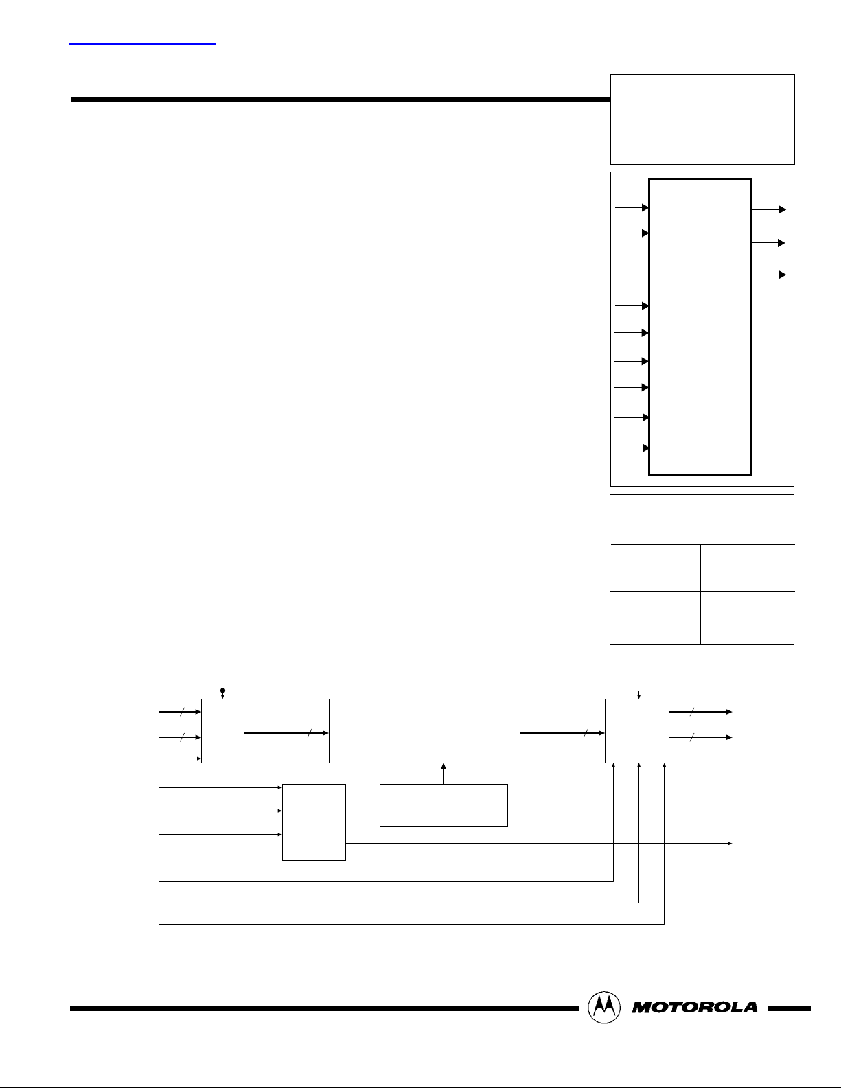
2K - Samples FFT-Processor
The MC92307 is a pipelined Fast Fourier Transformation (FFT) processor with a
blocklength of 2048 complex samples. It is especially designed for use in digital terrestrial Set-Top boxes according to the DVB-T standard for 2K transmission. One
block of 2048 complex samples can be processed in 224 µs
Feature Summary
• Processing of one block of 2048 complex samples (i.e. one 2K-OFDM symbol) in
224 µs.
• Designed for direct interfacing with Motorola’s OFDM demodulator MC92308.
• Input wordlength 8 bit, output accuracy selectable between 10 and 12 bit.
• Overflow on certain OFDM subcarriers due to co-channel interferes is handled internally.
• Readout of output samples can be shifted by half the blocklength to start at the
middle of the output block.
• Either multiplexed or non-multiplexed input and output format (the multiplexed
mode allows direct interfacing with Motorola’s OFDM Demodulator MC92308).
• Internal Bit reversal can be disabled to allow the construction of FFT modules for
blocklengths > 2K by using several devices in parallel.
• Low clock rate inputs and outputs.
• 0.5µm CMOS process at 3.3 V.
• 5 V tolerant inputs and outputs.
RESB
CLK
NOMUX
OFFSET
RES[1:0]
FFTSTART
DIN[7:0]
DINR[7:0]
SYMSYNC
DOUT[11:0]
DOUTR[11:0]
Ordering Information
Device
MC92307CI
Package
160QFP
NOMUX
DIN
8
Input
8DINR
FFTSTART
Preliminary Information
RESB
CLK
FFTSTART
OFFSET
RES[1:0]
REVRSB
Buffer
16 24
Control
FFT (11 stages)
incl. Rounding
Twiddle Factor ROM
Output
Reorder
Buffer
12 DOUT
12 DOUTR
SYMSYNC
Figure 1. Block diagram of the FFT processor MC92307
This document contains information on a new product.
Specifications and information herein are subject to change without notice.
MOTOROLA, INC. 1997 8/12/97

External Interfaces
Fast Fourier Transform in the DVB-T System
Within the DVB consortium several standards for digital
television broadcast were submitted for the different
transmission media, leading to DVB-S (satellite), DVBC (cable) and DVB-T (terrestrial). The details of the
DVB-T system are described in reference [1]. To cope
with the special effects of digital terrestrial transmission
the OFDM modulation scheme was chosen: In principle
the whole available bandwidth is divided into a large
number N (e.g. 2048) of separate narrowband subchannels (the OFDM subcarriers). Data associated with
each subcarrier are transmitted independently from and
in parallel with the other subcarriers, leading to a very
low datarate on each subcarrier compared to the overall
transmission capacity.
The superposition of all the subcarriers in the transmitter is achieved very efficiently by an IFFT. Consequently
the corresponding functional block in the receiver is a
FFT. This IFFT -> FFT pair is one of the central elements in all OFDM systems, it represents the link between the so-called frequency domain and the time
domain used for the RF link between the transmitter and
the receiver. Therefore one of the important parameters
describing an OFDM system is the blocklength of the
IFFT/FFT, such a block is called an ‘OFDM symbol’.
In the DVB-T specification two modes are described,
the first with 2048 (2K) complex samples per OFDM
symbol, the second with 8192 (8K) samples per block.
The MC92307 device described here is designed especially for the use in systems working according in the
2K-mode described in reference [1].
External Interfaces
Control Interface
CLK
The overall OFDM transmission clock of app.
36.57 MHz must be provided at this pin. Obviously in
case of a DVB-T frontend composed of a MC92308 together with the MC92307 both devices have to be supplied with the same clock signal. Normally the
36.57 MHz are generated by a VCXO in the tuner which
in turn is controlled by the OFDM timing synchronization
circuitry.
RESB
Synchronous Reset: Normally H, a L together with a rising edge at CLK puts all outputs in tri-state and aborts
any processing, leaving the FFT device in the idle
mode.
Preliminary Information
OFFSET
After the completion of the FFT processing the frequency domain data are output by the reorder buffer, starting
together with a pulse of the SYMSYNC pin. The starting
position of the output can be selected with the OFFSET
pin. With OFFSET set to L the first frequency domain
sample of a block that is delivered at the output of the
FFT device belongs the baseband frequency corresponding to the DC component (i.e. the center frequency in the received time domain signal). The numbers of
the frequency bins increases continuously until bin
#2047 at the end of the block.
If OFFSET is set to H the first frequency domain sample
belongs to the baseband frequency bin #1024, corresponding to an offset of one half of the block (i.e. the DC
component in the received time domain signal). Again
the bin numbers increase up to bin #2047. Then a wraparound to bin #0 occurs.
Table 1. Function of OFFSET
Sample #
after
SYMSYNC
s
0
s
1
... ... ...
s
1022
sd
1023
s
1024
... ... ...
s
2046
s
2047
(Baseband)
Bin #
(OFFSET = L)
DOUT
0
DOUT
1
DOUT
1022
DOUT
1023
DOUT
1024
DOUT
2046
DOUT
2047
(Baseband)
Bin #
(OFFSET = H)
DOUT
1024
DOUT
1025
DOUT
2046
DOUT
2047
DOUT
0
DOUT
1022
DOUT
1023
Note that the bin numbers given in the table above correspond to the baseband positions.
NOMUX
The input interface (DIN and DINR) and the output interface (DOUT and DOUTR) can be used in two modes:
Normally the complex samples are provided in the
MULTIPLEXED mode, i.e. at first the real part of one
sample is transferred using the DIN or DOUT lines followed by the imaginary part of the same sample using
the same physical pins. The pins labelled DINR and
DOUTR pins are not used, DINR should be tied to a
fixed value and DOUTR should be left unconnected.
The multiplexed mode is selected by setting the NOMUX line at L level, note that it is the only mode the FFT
device MC92307 can be used together with the OFDM
device MC92308.
MOTOROLA MC92307_DS - 8/12/97
2
External Interfaces
If NOMUX is set to H the real and imaginary part of one
sample is transferred in parallel using the DINR and
DOUTR lines for the real part and the DIN and DOUT
lines for the imaginary part. Consequently the transfer
rate is divided by 2 compared to the muxed mode at the
cost of more interconnection lines. Therefore this mode
is intended mainly for use with external devices that operate on lower rates.
REVRSB
To achieve the output of the frequency domain data in
natural order an internal bit reversal is done in the output reorder buffer. This bit reversal can be switched off
e.g. to allow the combination of 4 MC92307 devices together with an external final radix-4 butterfly stage to do
an 8K-FFT.
RES[1:0]
These two lines support the selection of the wordlength
at the FFT output:
Table 2. Output resolution selection
RES[1:0] DOUT[11:0]
00 [0, 0, d9, d8, ... ,d0, ]
01 [0, d
10 [d
11 Don’t care
, d9, d8, ... ,d0, ]
10
, d10, d9, d8, ... ,d0, ]
11
OFDM Device -> FFT Device
The figures below illustrate the input of the time domain
data into the FFT device and the output of the calculated frequency domain data after the completion of the
FFT. The samples belonging to the real part are denoted by ...r (real), the imaginary samples are marked with
...q (quadrature). Figure 2 applies for the Multiplexed
mode, Figure 3 is valid for the Non-multiplexed mode.
CLK
DIN
FFTSTART
DOUT
SYMSYNC
X0r X0q X1r X1q Xir Xq X(i+1)r X(i+1)q
Z(N-i)r Z(N-i)q Z(N-i+1)rZ(N-i+1)q Z0r Z0q Z1r Z1q
... ...
... ...
Preliminary Information
Figure 2. FFT Data I/O for the Multiplexed Mode
MC92307_DS - 8/12/97 MOTOROLA
3

CLK
External Interfaces
DINR
DIN
FFTSTART
DOUTR
DOUT
SYMSYNC
FFTSTART
The input of a data block into the FFT device starts with
a pulse of the FFTSTART signal. It must be delivered
together with the real part of the first time domain sample and should last 1..2 clock cycles.
DIN [7:0]
These pins accept the input data with a wordlength of
8 bit. In the muxed mode first the real part of a sample
must be provided followed by the imaginary part. In the
non-muxed mode only the imaginary part must be delivered to DIN. The data format is fixed to 2’s complement.
DINR [7:0]
In the non-muxed mode (NOMUX = H) the real part of
the input samples is entered into the FFT device via
these pins (they should be connected to a fixed level if
the muxed mode is used). As the DIN inputs these inputs expect 2’s complement format.
X0r X1r Xir X(i+1)r
X0q X1q Xiq X(i+1)q
Z(N-i)r Z(N-i+1)r Z0r Z1r
Z(N-i)q Z(N-i+1)q Z0q Z1q
Figure 3. Data I/O for the Non-multiplexed Mode
Preliminary Information
... ...
...
...
... ...
... ...
FFT Device -> OFDM Device
SYMSYNC
The start of the output of a FFT block after processing
is indicated by a pulse of the SYMSYNC signal with a
duration of 2 clock cycles. It is delivered together with
the real part of the first output sample.
DOUT [11:0]
These pins deliver the output data of the FFT device in
2’s complement format. In the non-muxed mode
(NOMUX = H) the real part of the samples is followed by
the imaginary part. In the muxed mode only the imaginary parts appears at the DOUT pins.The valid bits are
adjusted using the RES pins, see above.
DOUTR [11:0]
In the non-muxed mode (NOMUX = H) the real part of
the output samples appears at these pins in 2’s complement format. The wordlength selection by the RES pins
is also valid for DOUTR. If the non-muxed mode is used
these pins may be left unconnected.
MOTOROLA MC92307_DS - 8/12/97
4

Pinout
Motorola’s FFT device is packaged into a 160QFP
package. The pinout of this package as well as the input
and output lines are given in Figure 4 and Table 3.
reserved (open)
reserved (open)
reserved (VSS)
VDD
reserved (VSS)
reserved (VSS)
reserved (VSS)
reserved (VSS)
reserved (VSS)
VDD
reserved (VSS)
160QFP
reserved (open)
reserved (open)
reserved (open)
reserved (open)
reserved (open)
reserved (open)
reserved (open)
reserved (open)
reserved (open)
reserved (open)
reserved (open)
reserved (open)
reserved (open)
reserved (open)
reserved (open)
reserved (open)
reserved (open)
reserved (open)
reserved (open)
reserved (open)
reserved (open)
reserved (VSS)
reserved (open)
reserved (open)
reserved (open)
VDD
VDD
VSS
VSS
VDD
VSS
CLK
VSS
OFFSET
VDD
DINR7
DINR6
VSS
DINR5
DINR4
reserved (open)
VSS
reserved (open)
reserved (VSS)
reserved (VSS)
VSS
The supply voltage of the IC is 3.3 V, its power consumption will be app. 0.75 W in a typical DVB-T application as it is described in “Application Information’.
reserved (VSS)
reserved (VSS)
RESB
reserved (VSS)
REVRSB
reserved (VSS)
reserved (VSS)
reserved (VSS)
reserved (VSS)
reserved (VSS)
VSS
reserved (VSS)
VDD
reserved (VSS)
reserved (VSS)
reserved (VSS)
reserved (VSS)
VSS
reserved (VSS)
reserved (VSS)
reserved (VSS)
reserved (VSS)
reserved (VSS)
reserved (VSS)
VDD
reserved (VSS)
reserved (VSS)
reserved (VSS)
VSS
reserved (VSS)
reserved (VSS)
reserved (VSS)
reserved (VSS)
reserved (VSS)
reserved (VSS)
reserved (VSS)
VDD
reserved (VSS)
reserved (VSS)
reserved (VSS)
reserved (VSS)
reserved (VSS)
VSS
reserved (VSS)
reserved (VSS)
reserved (VSS)
VDD
VSS
reserved (VSS)
RES1
RES0
NOMUX
DOUTR0
DOUTR1
VDD
DOUTR2
DOUT3
VSS
DOUTR4
DOUTR5
VDD
DOUTR6
DOUTR7
DINR3
DINR2
VDD
DINR1
DINR0
VSS
DIN7
DIN6
VDD
DIN5
DIN4
DIN3
VSS
DIN2
DIN1
DIN0
VDD
DOUT11
FFTSTART
SYMSYNC
VSS
DOUT10
DOUT9
DOUT8
DOUT7
VDD
DOUT6
DOUT5
DOUT4
DOUT3
VSS
DOUT2
DOUT1
VDD
DOUT0
DOUTR11
VSS
DOUTR9
DOUTR8
DOUTR10
Preliminary Information
Figure 4. Pinout of the MC92307
MC92307_DS - 8/12/97 MOTOROLA
5

Pinout
Table 3. MC92307 Pin Description of the FFT device
SIGNAL FUNCTIONALITY
RESB Synchronous Reset (active low)
CLK 36.57 MHz clock
REVRSB Enable bit reversal (active low)
DIN[7:0] Complex data input muxed (real component first)
RES[1:0] Output resolution selection
OFFSET Selection of half symbol rotation in output
FFTSTART Input frame start
DOUT[11:0] Complex data output muxed (real component first)
SYMSYNC Output frame start
NOMUX Selection of non-multiplexed data busses
DINR[7:0] Complex data input (real part) if NOMUX = 1
DOUTR[11:0] Complex data output (real part) if NOMUX = 1
Preliminary Information
MOTOROLA MC92307_DS - 8/12/97
6

Package Data
The mechanical dimensions of the 160QFP package
that is used for the FFT device are shown below:
NOTES:
1. DIMENSIONING AND TOLERANCING PER ANSI Y14.5M, 1982.
2. CONTROLLING DIMENSION: MILLIMETER.
3. DATUM PLANE -H- IS LOCATED AT BOTTOM OF LEAD AND IS COINCIDENT WITH THE LEAD WHERE THE LEAD EXITS THE
PLASTIC BODY AT THE BOTTOM OF THE PARTING LINE.
4. DATUMS -A-, –B- AND -D- TO BE DETERMINED AT DATUM PLANE -H-.
5. DIMENSIONS S AND V TO BE DETERMINED AT SEATING PLANE -C-.
6. DIMENSIONS A AND B DO NOT INCLUDE MOLD PROTRUSION. ALLOWABLE PROTRUSION IS 0.25 (0.010) PER SIDE. DIMENSIONS A AND B DO INCLUDE MOLD MISMATCH AND ARE DETERMINED AT DATUM PLANE -H-.
7. DIMENSION D DOES NOT INCLUDE DAMBAR PROTRUSION. ALLOWABLE DAMBAR PROTRUSION SHALL BE 0.08 (0.003) TOTAL IN EXCESS OF THE D DIMENSION AT MAXIMUM MATERIAL CONDITION. DAMBAR CANNOT BE LOCATED ON THE LOWER RADIUS OR THE FOOT.
MC92307_DS - 8/12/97 MOTOROLA
Preliminary Information
Figure 5. Mechanical Data of the 160QFP Package
7

Application Information
As already mentioned the FFT device is especially suited to be combined with Motorola’s OFDM device
MC92308 to form the complete digital part of a frontend
for a 2K DVB-T receiver. Refer to Figure 6 for the functional blocks of a terrestrial DVB receiver. Further details of the blocks are given in reference [2].
One of the key signals for the successful reception of an
OFDM signal is the correct timing synchronization, that
means that the synchronization circuitry chooses the
8 12
FFTDO FFT
CLK
CTLP
START
Tuner
Core
A
1/2
RESB
ADCDATA
8
D
CLKEN18
CLK
correct starting point to trigger the FFT operation.
Therefore the OFDM demodulator MC92308 provides
the FFTSTART signal to the FFT device. If 2048 complex time domain samples have been read into the input
buffer the FFT operation starts. Its result is flagged with
the SYMSYNC line and the calculated frequency domain samples are output to the OFDM device that continues with the demodulation process.
MC92307
2k-FFT
2
IC
MC92308
OFDM
CLK
AGC
CTLN
CTLP
AGC
CTLN
FFTDISYMSYNC
MBUS
uP IF
DVALID
FECCLK
G1DATA
G2DATA
16
3
3
HC05
uC
MC92309
FEC
MPEG Clock
MPEG-2
8
Transport
Stream
Tuner
~
VCO
Figure 6. Application Example for the OFDM and FFT Devices
Preliminary Information
MOTOROLA MC92307_DS - 8/12/97
8

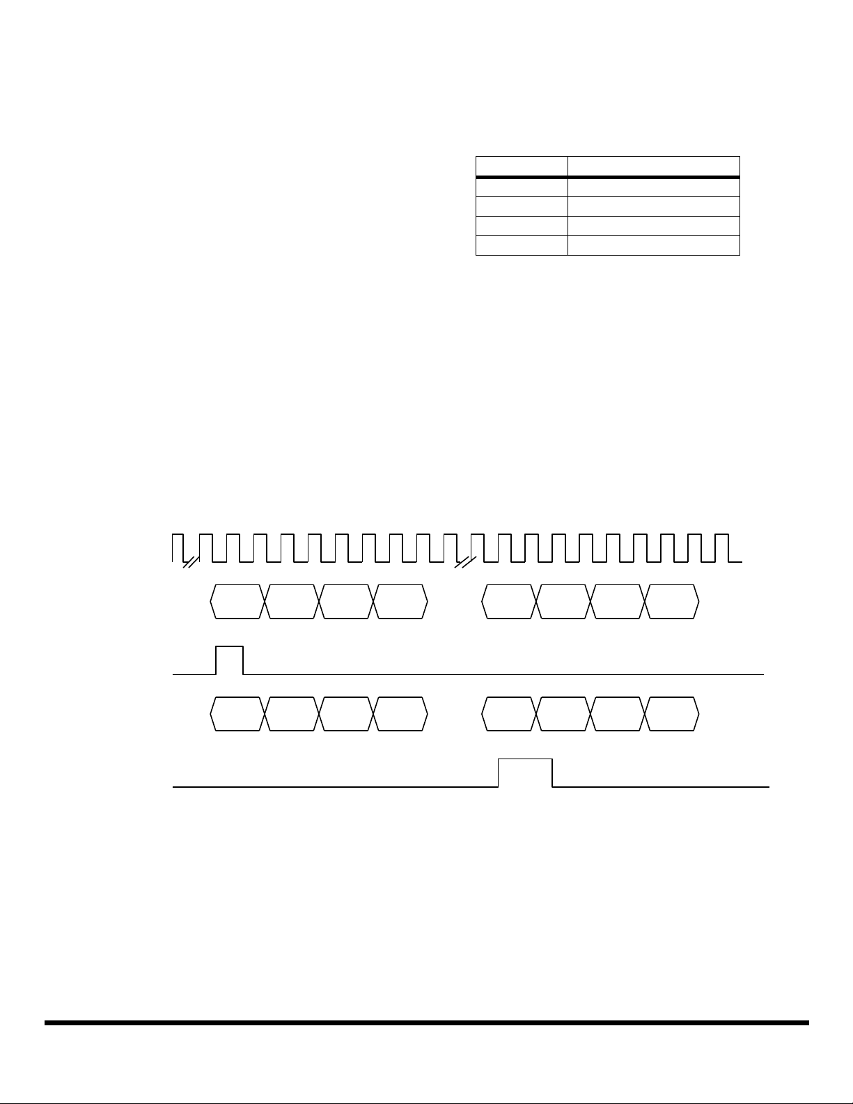
Switching Characteristics
In the following diagram together with the associated table the characteristics of the interface for the FFT data
is given. Note that they are valid for temperatures be-
7
CLK
2
1
FFTSTART
3
DIN
5
4
IIQQ
00 00
5
tween 0°C and 80°C and a supply voltage range of
3.0 V - 3.6 V
444
SYMSYNC
DOUT
No. Characteristic min max unit
1 FFTSTART to CLK setup time 1.4 ns
2 FFTSTART to CLK hold time 3.1 ns
3 Data in to CLK setup time 2.3 ns
4 Data in to CLK hold time 3.5 ns
5 CLK to SYMSYNC out delay 4.6 13.1 ns
6 CLK to Data out delay 3.6 11.8 ns
7 CLK period 27.4 ns
6
IIQQ
00 00
Figure 7. Timing Characteristic of the FFT Device
Table 4. Timing Data for the FFT Device
6666
Preliminary Information
MC92307_DS - 8/12/97 MOTOROLA
9

References
[1] Digital broadcasting systems for television, sound
and data services; Framing structure, channel coding
and modulation for digital terrestrial television. Draft
prETS 300 744 published by ETSI September 1996.
[2] MC92308 OFDM Demodulator, Product Data
Sheet for the MC92308.
Preliminary Information
Motorola reserves the right to make changes without further notice to any products herein. Motorola makes no warranty, representation or guarantee regarding the
suitability of its products for any particular purpose, nor does Motorola assume any liability arising out of the application or use of any product or circuit, and
specifically disclaims any and all liability, including without limitation consequential or incidental damages. “Typical” parameters which may be provided in Motorola
data sheets and/or specifications can and do vary in different applications and actual performance may vary over time. All operating parameters, including
“Typicals” must be validated for each customer application by customer’s technical experts. Motorola does not convey any license under its patent rights nor the
rights of others. Motorola products are not designed, intended, or authorized for use as components in systems intended for surgical implant into the body, or other
applications intended to support or sustain life, or for any other application in which the failure of the Motorola product could create a situation where personal injury
or death may occur. Should Buyer purchase or use Motorola products for any such unintended or unauthorized application, Buyer shall indemnify and hold
Motorola and its officers, employees, subsidiaries, affiliates, and distributors harmless against all claims, costs, damages, and expenses, and reasonable attorney
fees arising out of directly or indirectly, any claim of personal injury or death associated with such unintended or unauthorized use, even if such claim alleges that
Motorola was negligent regarding the design or manufacture of the part. Motorola and are registered trademarks of Motorola, Inc. Motorola, Inc. is an Equal
Opportunity/Affirmative Action Employer.
How to reach us:
USA/EUROPE/Locations Not Listed: Motorola Literature Distribution; JAPAN: Nippon Motorola Ltd.; Tatsumi-SPD-JLDC, 6F Seibu-Butsuryu-Center,
P.O. Box 5405, Denver Colorado 80217. 1-800-441-2447 or 303-675-2140 3-14-2 Tatsumi Koto-Ku, Tokyo 135, Japan. 81-3-3521-8315
TM
: RMFAX0@email.sps.mot.com -TOUCHTONE (602) 244-6609 ASIA/PACIFIC: Motorola Semiconductors H.K. Ltd.; 8B Tai Ping Industrial Park,
MFax
INTERNET:http://mot-sps.com/sps/General/sales.html 51 Ting Kok Road, Tai Po, N.T., Hong Kong. 852-26629298
MC92307_DS - 8/12/97
 Loading...