

查询MC92305供应商
MOTOROLA
SEMICONDUCTOR TECHNICAL DATA
Product Preview
16/32/64/128/256 QAM RECEIVER AND
REED-SOLOMON DECODER
The MC92305 is a high performance digital demodulator/decoder optimized for
demodulation and block error correction of QAM signals used in Digital Video Broadcast by Cable (DVB-C) and DAVIC 1.0 compliant applications.
Feature Summary
• Single A/D IF interface
• Maximum signaling rate of 7Mbaud (42Mbits/sec for 64 QAM and
56Mbits/sec for 256 QAM)
• DVB compliant QAM Coherent Demodulator
• Transversal/Decision Feedback adaptive equalizer
No external components or control required
• Micro-reflection cancellation up to 1.4µs
• Nyquist baseband filtering (α=0.15)
• 1-bit Σ∆ control outputs for AGC, VCO and optional external NCO
• Programmable De-Interleaving For MPEG Transport Packets
• DVB Compliant (204,188,16) Reed Solomon Decoding
• DVB Compliant PRBS Descrambling
• 0.5 micron CMOS, 3.3V technology
•I2C Interface for control/monitoring of system
Current Information @ www.mot.com/ADC
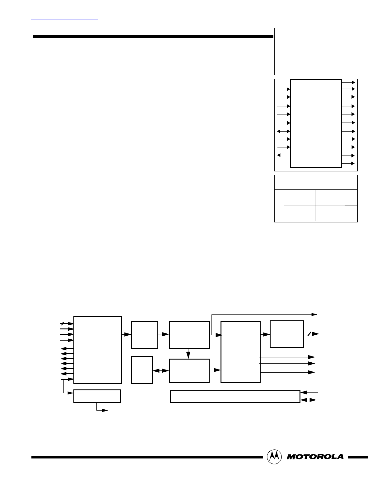
MC92305
AGCOUT
RESETB
I&Q[9:0]
IQSWAP
ADCLKIN
SYMFE
SDATA
IN_FMT
SCLK
BITCLK
Ordering Information
Device
MC92305CD
ADCLKOUT
VCOOUT
CTLOUT
DMODLOCK
MSSLOCK
DOUT[7:0]
DO_VAL
FRAME_SYNCH
FRAME_ERR
FRAME_START
Package
80QFP
FRAME_SYNCH
8
DOUT
FRAME_START
FRAME_ERR
DO_VAL
SCLK
SDATA
I &Q
SYMFE
RESETB
IN_FMT
ADCLKOUT
CTLOUT
VCOOUT
AGCOUT
MSSLOCK
DMODLOCK
ADCLKIN
10
16/32/64/128/256
QAM DEMOD.
APLL
BITCLK
Symbol
To Byte
Mapping
RAM
Synch Word
Synchronization
Programmable
De-Interleaver
Reed-Solomon
Decoder
2
I
C Interface
PRBS
Descrambler
Figure 1. MC92305 Block Diagram
This document contains information on a product under development. Motorola reserves the right to change or discontinue this product without notice.
MOTOROLA, INC. 1997 4/9/97

Demodulator Interface
The MC92305 is interfaced to a single 8-bit (10-bit for
256 QAM) A/D converter which is clocked at 4 times the
symbol rate (4Rs). A pin-programmable input format selector allows the use of A/D converters which produce output samples in either offset binary or 2's complement
format.
The demodulator function performs all required signal processing to extract the I and Q symbols from the received data stream. Fully internal digital clock recovery/
synchronization, Nyquist filtering and LTE/DFE adaptive
equalization are employed to recover symbol information
in the presence of channel noise and micro-reflections.
The equalizer is able to converge with random received
data and no special training sequence is required.
Single-bit (Sigma-Delta converted) outputs are provided for automatic gain control (AGC) and A/D voltage
controlled oscillator(VCO) feedback functions within the
external IF circuitry.
De-Interleaving
After synchronization with the MPEG framing structure the data stream is convolutionally de-interleaved. To
obtain the maximum data throughput (i.e. minimum latency) under various channel SNR's the de-interleaver
can be programmed.
Table 1 describes the usable parameter settings
with varying delay (latency) and burst (error correction).
N is the block size in bytes, DEPTH is the number of
paths in the de-interleaver and INC is the increment (in
bytes) in which data is moved through the de-interleaver
paths. DELAY is defined as the latency (in bytes) in the
de-interleaver (after frame synchronization has been
achieved) and BURST is defined as the maximum number of bytes that can be affected by bursty noise before
more than eight bytes are corrupted in a de-interleaved
MPEG frame. Minimum burst error correction of 8 bytes
is guaranteed by the Reed Solomon decoder.
Table 1. De-Interleaver Configurations
The demodulator carrier tracking loop is capable of
locking to signals which contain moderate frequency offsets (0.06Rs) from the specified IF frequencies. The carrier tracking loop is normally closed digitally, using an
internal numerically controlled oscillator (NCO) but a single bit control output is also provided for closing the loop
through an external VCO.
External signals indicate when the demodulator has
successfully acquired the data stream and recovered the
data clock (MSSLOCK), and when the received symbols
are consistently below a programmable error threshold
(DMODLOCK).
Symbol To Byte Mapping
The received symbols are mapped into bytes according to the DVB/Davic 1.0 specifications. An internal I2C
register can be used to select an alternative de-coding
scheme which is specified as a mask programmable option.
Sync Word Synchronization.
After demodulation of the received data, the byte
stream is examined for MPEG synchronization (inverted
and non-inverted) bytes and when the number detected
exceeds programmable thresholds, the received byte
stream is recognized as valid MPEG data.
FRAME_SYNCH is asserted when the programmed number of synchronization bytes have been recognized.
FRAME_START is asserted for one byte width at the start
of each MPEG frame.
N Depth Inc Delay Burst
1110 8
204 4 51 612 30
204 6 34 1020 44
102 17 6 1632 54
204 12 17 2244 86
The operation of the de-interleaver is software con-
figurable via the I2C interface during system operation.
Reed Solomon Decoding
The Reed Solomon decoder block implements a
shortened Reed-Solomon decoder with field generator
polynomial X8 + X4 + X3 + X2 + 1 as per the DVB specification.
The decoder is able to correct up to 8 byte errors in
each received packet. Following error correction the
Reed Solomon decoder outputs the MPEG packets and
asserts the DO_VAL output for each byte output (50%
duty cycle per byte).
If the error correcting ability of the Reed Solomon
decoder is exceeded (more than 8 byte errors in a single
packet), the original, uncorrected, data is output and the
DO_VAL output is not asserted. The FRAME_ERR signal is asserted for the duration of the uncorrected MPEG
frame.
MOTOROLA MC92305
2 Rev.1.1

PRBS Descrambling
The error corrected data from the Reed Solomon
decoder is de-randomized using a PRBS generator
with polynomial 1 + X14 + X15. The PRBS generator is
initialized every 8 MPEG transport packets with the value 100101010000000 as per the DVB specification.
I2C Interface
In accordance with the I2C specification, the I2C
master (host microprocessor) initiates all data transfers
to and from the demodulator and provides the I2C
clock. Data is always transferred one byte at a time,
MSB first, and the receiver must acknowledge each
byte by pulling the data line low during the cycle following the LSB (acknowledge cycle). The demodulator interprets the byte following its slave address as an 8-bit
sub-address which selects a particular register to be
written to or read from. The I2C data pin is bidirectional
and is driven by an open-drain output in the MC92305.
External pull-up resistors are required to implement the
wired-AND function on each of these signals, per the
I2C bus specification.
Σ∆ Interfaces
The single-bit outputs which interface to analog
circuits are VCOOUT, AGCOUT and CTLOUT. These
are the loop filter outputs for the MSS symbol sync,
AGC and Carrier Tracking Loop, respectively. The digital sigma-delta converters which drive these outputs
have programmable output sampling rates up to a maximum of 4.0Rs. The bandwidths of each of these loops
and the output sampling rates of the loops (input sampling rates of the sigma-delta converters) are programmable. The sigma-delta output sampling rates should
be commensurate with the loop bandwidths and loop
output sampling rates selected.
Software-Configurable Items
The command interfaces can address a variety of
internal registers to configure most critical demodulator
and decoder parameters. These include: all loop bandwidths, equalizer tap values and equalizer control (load
taps and adapt, load taps and freeze, adapt without
loading and freeze without loading), the filter coefficients of the receive lowpass filter, the lock detector
thresholds for MSS lock and Carrier lock, the center tap
fixed gain adjustment, the NCO frequency preset, software reset (which performs the same function as the
hardware power-on reset), upper and lower limits on
the NCO frequency and, input and output sampling
rates of each digital sigma-delta converter.
Software-Readable Items
All of the software-configurable registers are also
readable. This is intended to allow the host to interrogate the demodulator prior to changing parameters.
There are also a number of demodulator registers
which are read-only and are intended to provide useful
demodulator status information to the host for monitoring and debugging purposes. These include: NCO frequency (which provides an indirect measurement of the
frequency error in the channel tuner and modem local
oscillators), AGC control value (an indicator of received
signal power), constellation variance (an indicator of received energy per symbol to noise power spectral density) Es/No, (used in generating the carrier lock detect
signal) and, MSS control value (which provides an indirect measurement of baud rate error and is used in generating the MSS lock detect signal).
Pin-Programmable Interfaces
A variety of functions are selectable by hard-wiring
MC92305 pins to VDD or VSS, rather than via the I2C
interface. These fall in the category of functions which
will seldom be changed once a particular application
circuit is debugged and functioning correctly. The pin
programmable features are:
• IQSWAP - Swap internal I and Q data paths
• IN_FMT - Specify A/D output data format (two’s
complement or offset binary)
• SYM_FE - specify which edge of the output symbol
clock is to be aligned with the symbols.
• TSTMODE - Used during production testing of the
device but can also be used to disable and bypass
certain of the functions in the MC92305.
MC92307 MOTOROLA
Rev.1.1 3

Pin Description
SIGNAL Type FUNCTIONALITY
RESETB Input Power On Reset
I[9:0] & Q[9:0] Input IF I & Q Symbol Input
ADCLKIN Input Input Clock (4Rs)
IN_FMT Input Input Format Selection
IQSWAP Input Interchanges I and Q
SYMFE Input Data to Clock Edge Relationship Control
BITCLK Output Data Output Clock
AGCOUT, VCOOUT, CTLOUT Output AGC, MSS and Carrier Tracking Loop Control
ADCLKOUT Output A/D Clock Output (4Rs)
DMODLOCK Output Carrier and Equalizer Lock Detection
MSSLOCK Output Carrier Lock Detection
SCLK Output Symbol Clock Output
DOUT[7:0] Output Decoded Output Data
DO_VAL Output Data Output Valid
FRAME_START Output MPEG Frame Start Indicator
FRAME_SYNCH Output MPEG Frame Synchronizer Lock Detection
FRAME_ERR Output Uncorrected Reed Solomon Errors Indicator
SDATA I/O Data Bus of I
SCLK I/O Clock Line of I
Table 2. MC92305 Pin Description
2
C-interface
2
C-interface
Motorola reserves the right to make changes without further notice to any products herein. Motorola makes no warranty, representation or guarantee regarding the
suitability of its products for any particular purpose, nor does Motorola assume any liability arising out of the application or use of any product or circuit, and
specifically disclaims any and all liability, including without limitation consequential or incidental damages. “Typical” parameters which may be provided in Motorola
data sheets and/or specifications can and do vary in different applications and actual performance may vary overtime. All operating parameters, including “Typicals”
must be validated for each customer application by customer’s technical experts. Motorola does not convey any license under its patent rights nor the rights of
others. Motorola products are not designed, intended, or authorized for use as components in systems intended for surgical implant into the body, or other
applications intended to support or sustain life, or for any other application in which the failure of the Motorola product could create a situation where personal injury
or death may occur. Should Buyer purchase or use Motorola products for any such unintended or unauthorized application, Buyer shall indemnify and hold
Motorola and its officers, employees, subsidiaries, affiliates, and distributors harmless against all claims, costs, damages, and expenses, and reasonable attorney
fees arising out of directly or indirectly, any claim of personal injury or death associated with such unintended or unauthorized use, even if such claim alleges that
Motorola was negligent regarding the design or manufacture of the part. Motorola and
Opportunity/Affirmative Action Employer.
How to reach us:
USA/EUROPE/Locations Not Listed: Motorola Literature Distribution; JAPAN: Nippon Motorola Ltd.; Tatsumi-SPD-JLDC, 6F Seibu-Butsuryu-Center,
P.O. Box 20912; Phoenix, Arizona 85036. 1-800-441-2447 or 602-303-5454 3-14-2 Tatsumi Koto-Ku, Tokyo 135, Japan. 03-81-3521-8315
MFAX: RMFAX0@email.sps.mot.com -TOUCHTONE (602) 244-6609 ASIA/PACIFIC: Motorola Semiconductors H.K. Ltd.; 8B Tai Ping Industrial Park,
INTERNET: http://Design-NET.com 51 Ting Kok Road, Tai Po, N.T., Hong Kong. 852-26629298
b are registered trademarks of Motorola, Inc. Motorola, Inc. is an Equal
MOTOROLA MC92305
4 Rev.1.1
 Loading...