

查询MC92303供应商
MOTOROLA
SEMICONDUCTOR TECHNICAL DATA
Product Brief
QPSK/BPSK DIGITAL DEMODULATOR
Current Information@www.mot.com/ADC
MC92303
The MC92303 is a coherent digital demodulator for QPSK and BPSK modulated
signals utilized in Digital-TV applications according to the EBU defined DVB transmission standard for satellite Set-Top systems or similar. The MC92303 contains all the
functionality required to lock onto signals with frequency offsets as large as the baud
rate and extract the desired signal from a frequency band with adjacent channel interference and other undesirable signals.
Feature Summary
• DVB compliant QPSK/BPSK Coherent Demodulator
• Variable Modulation Rate up to 30 MBaud to work with all present European DVB
Channels
• Selectable Input Format (Offset Binary/2’s Complement)
• DC Offset Removal, I/Q-swapping and Input Format Selection in one block
• Decimation Filters for Oversampling Ratios of 2/T, 3/T, 4/T, 6/T, 8/T, 12/T and 16/T
• Half Nyquist Baseband Filters (α=0.35)
• Internal Numerically Controlled Oscillator (NCO)
• Automatic Gain Control (AGC) provided to analog front-end
• Automatic Frequency Control (AFC) to ±Rs (Symbol Rate)
• Clock Synchronization with 1-Bit Σ∆-Converter Output for ADC control
• Programmable Second Order Loop Filters for Carrier Recovery and AGC
• 3-bit Soft Decision output per Symbol with selectable format (Offset Binary/2’s
Complement/Sign Magnitude)
• Programmable Sampling Rates of the Digital Sigma-Delta Converters
• < 0.5 dB Implementation Loss from theory
•I2C Programmable Interface
• 0.5µ CMOS Process at 3.3V
RESET
I,Q[5:0]
CLK_VCO
FORMAT
SDA
SADR[6:0]
SCL
CLK
VCO
AGC
Q_soft[2:0]
I_soft[2:0]
Ordering Information
Device
MC92303BT
Package
160QFP
AGC
Control
I
Q
SDA
SCL
SADR
Σ∆
6
6
7
DC-
Removal
2
C
I
Interface
Parameters
AGC
Loop Filter
cosΘ
Complex
Multiplier
sinΘ
NCO
Decimation
Filter
Digital AGC
Sweep /
Carrier
Loop Filter
Ext. Clkref.
Half Nyquist
False Lock Detector
Phase Lock Detector
Filter
AFC / Clock
Synchron.
Σ∆
8/3 Bit Mapper
Data
Estimator
VCO
Control
3
I_soft
3
Q_soft
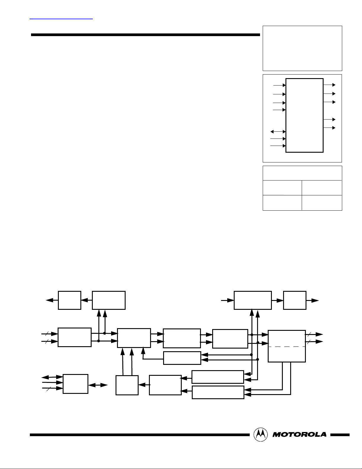
Figure 1. QPSK/BPSK Demodulator Block Diagram
This document contains information on a new product.
Specifications and information herein are subject to change without notice.
MOTOROLA, INC. 1997 4/10/97
Control Loops
The inputs to the device are 6 bit I and Q digital
signals. A pin programmable input format selector allows use of A/D converters with either offset binary or
2’s complement output format. The A/D output data is
fed into the carrier synchronization loop which is capable of locking onto signals with frequency offsets as
large as the baud rate. The carrier synchronizer includes a complex multiplier, a phase detector, a programmable second order loop filter, a phase lock
detector, a false lock detector and a frequency sweep
function. The carrier tracking loop is closed digitally using an internal numerically controlled oscillator (NCO).
The frequency sweep rate, the frequency sweep limit,
the phase and frequency lock detector thresholds and
the loop parameters are programmable. The I and Q
QPSK symbols produced in this loop are further processed by a Decimation Filter and a Half Nyquist Filter
(roll-off factor of 0.35) to perform the matched filtering.
Once processed, the filtered data samples are passed
to the data estimator which produces 3 bits of I and Q
soft decision data (device output) as well as I and Q error vectors.
The demodulator also performs a non-coherent
automatic gain control (AGC) function on the IF signal
using a total power algorithm and generates a single bit
output signal which must be lowpass filtered and interfaced to the gain control port of a variable gain amplifier. The AGC includes a programmable second order
loop filter.
Another control loop, the mid-symbol sampling
synchronization loop, ensures that the optimum A/D
sampling times are determined by providing a single bit
output signal to a voltage controlled oscillator (VCO)
clock generator. This VCO quiescent frequency is automatically set to 2, 3, 4, 6, 8,12 or 16 Rs depending on
from LNB
1st IF Freq.
0.95 - 2.15 GHz
Freq.
Synthesizer
2nd IF Freq.
480 MHz
0°
90°
the oversampling factor. Its output signal levels must be
suitable for clocking both the A/D converter and the
QPSK demodulator.
Decimation Filter
The Decimation Filter block consists of three switchable decimation filters: two 1/2-band filters and a 2/3band filter. Together with a switchable input decimation
of 2, the decimation filter block enables the demodulator to operate at an oversampling ratio of 2, 3, 4, 6, 8,
12, or 16. The variable sampling demodulator minimizes the external components to build a Set Top box for
the whole range of data rates. In order to compensate
different signal gains after the decimation an internal
Digital AGC produces a control signal which adjusts the
gain after the complex multiplier.
I2C interface
The MC92303 is a slaved device that is intended
to be controlled via the I2C interface. In accordance
with the I2C specification, the I2C master initiates all
data transfers to and from the demodulator and provides the I2C clock. Data is always transferred one byte
at a time, MSB first, and the receiver must acknowledge
each byte by pulling the data line low during the cycle
following the LSB. The demodulator interprets the byte
following its slave address as an 8-bit sub-address
which selects a particular register to be written to or
read from.
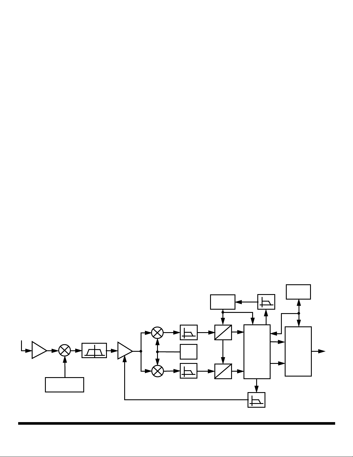
Application
The demodulator can be used to implement a DVB
compliant demodulator with the circuitry shown in Figure 2. The 3 bit soft decision data of the demodulator is
connected directly toa Viterbi Decoder or a combined
Viterbi and Reed Solomon Decoder.
Host
CPU
MC92302
VI1[2:0]
DO[7:0]
VI0[2:0]
Freq. = 0 Hz
LO
Clock
VCO
A
A
D
D
VCO
I[5:0]
SDA
I_soft[2:0]
MC92303
Q_soft[2:0]
Q[5:0]
AGC
2
I
C
Figure 2. DVB Application Example
MOTOROLA MC92303
2 Rev.1.3

Table 1. MC92303 Pin Description
SIGNAL FUNCTIONALITY
RESET Asynchronous Reset
2
SDA Data Bus of I
SADR[6:0] Slave Address of I
SCL Clock Line of I
I,Q[5:0] Inphase and Quadrature Symbol Inputs
CLK_VCO Input Clock from VCO
FORMAT Input Format Selection
I_soft[2:0],
Q_soft[2:0]
Soft Decision Output Signals
BPSK Demodulated BPSK Signal
AGC AGC Control Signal
VCO Control Signal for External VCO
CLK Control Signal for Clock VCO
C-interface
2
C-interface
2
C-interface
Motorola reserves the right to make changes without further notice to any products herein. Motorola makes no warranty, representation or guarantee regarding the
suitability of its products for any particular purpose, nor does Motorola assume any liability arising out of the application or use of any product or circuit, and
specifically disclaims any and all liability, including without limitation consequential or incidental damages. “Typical” parameters which may be provided in Motorola
data sheets and/or specifications can and do vary in different applications and actual performance may vary over time. All operating parameters, including
“Typicals” must be validated for each customer application by customer’s technical experts. Motorola does not convey any license under its patent rights nor the
rights of others. Motorola products are not designed, intended, or authorized for use as components in systems intended for surgical implant into the body, or other
applications intended to support or sustain life, or for any other application in which the failure of the Motorola product could create a situation where personal injury
or death may occur. Should Buyer purchase or use Motorola products for any such unintended or unauthorized application, Buyer shall indemnify and hold
Motorola and its officers, employees, subsidiaries, affiliates, and distributors harmless against all claims, costs, damages, and expenses, and reasonable attorney
fees arising out of directly or indirectly, any claim of personal injury or death associated with such unintended or unauthorized use, even if such claim alleges that
Motorola was negligent regarding the design or manufacture of the part. Motorola and are registered trademarks of Motorola, Inc. Motorola, Inc. is an Equal
Opportunity/Affirmative Action Employer.
How to reach us:
USA/EUROPE/Locations Not Listed: Motorola Literature Distribution; JAPAN: Nippon Motorola Ltd.; Tatsumi-SPD-JLDC, 6F Seibu-Butsuryu-Center,
P.O. Box 5405, Denver Colorado 80217. 1-800-441-2447 or 303-675-2140 3-14-2 Tatsumi Koto-Ku, Tokyo 135, Japan. 81-3-3521-8315
MFax: RMFAX0@email.sps.mot.com -TOUCHTONE (602) 244-6609 ASIA/PACIFIC: Motorola Semiconductors H.K. Ltd.; 8B T ai Ping Industial P ark,
INTERNET:http://mot-sps.com/sps/General/sales.html 51 Ting Kok Road, Tai Po, N.T., Hong Kong. 852-26629298
MC92303
 Loading...