

Motorola MC88921DW Datasheet
SEMICONDUCTOR TECHNICAL DATA
# #
"
### !
Order this document
from Logic Marketing
The MC88921 Clock Driver utilizes phase–locked loop technology to
lock its low skew outputs’ frequency and phase onto an input reference
clock. It is designed to provide clock distribution for CISC microprocessor
or single processor RISC systems.
The PLL allows the high current, low skew outputs to lock onto a single
clock input and distribute it with essentially zero delay to multiple
locations on a board. The PLL also allows the MC88921 to multiply a low
frequency input clock and distribute it locally at a higher (2X) system
frequency.
• 2X_Q Output Meets All Requirements of the 20, 25 and 33MHz 68040
Microprocessor PCLK Input Specifications
• 60 and 66MHz Output to Drive the Pentium Microprocessor
• Four Outputs (Q0–Q3) With Output–Output Skew <500ps and Six
Outputs Total (Q0–Q3, 2X_Q) With <1ns Skew Each Being Phase and
Frequency Locked to the SYNC Input
• The Phase Variation From Part–to–Part Between SYNC and the ‘Q’
Outputs Is Less Than 600ps (Derived From the TPD Specification,
Which Defines the Part–to–Part Skew)
• SYNC Input Frequency Range From 5MHZ to 2X_Q F
Max
/4
• Additional Outputs Available at 2X the System ‘Q’ Frequency
• All Outputs Have ±36mA Drive (Equal High and Low) CMOS Levels.
Can Drive Either CMOS or TTL Inputs. All Inputs Are TTL–Level
Compatible
• Test Mode Pin (PLL_EN) Provided for Low Frequency Testing
• Special Power–Down Mode With 2X_Q, Q0, and Q1 Being Reset (With
MR
), and Other Outputs Remain Running. 2X_Q, Q0 and Q1 Are
Guaranteed to Be in Lock 3 Clock Cycles After MR
Is Negated
LOW SKEW CMOS PLL
CLOCK DRIVER
With Power–Down/
Power–Up Feature
20
1
DW SUFFIX
SOIC PACKAGE
CASE 751D–04
Four ‘Q’ outputs (Q0–Q3) are provided with less than 500ps skew between their rising edges. A 2X_Q output runs at twice the
‘Q’ output frequency. The 2X_Q output is ideal for 68040 systems which require a 2X processor clock input. The 2X_Q output
meets the tight duty cycle spec of the 20, 25 and 33MHz 68040. The 66MHz 2X_Q output can also be used for driving the clock
input of the Pentium Microprocessor while providing multiple 33MHz outputs to drive the support and bus logic. The FBSEL pin
allows the user to internally feedback either the Q or the Q/2 frequency providing a 1x or 2x multiplication factor of the reference
input.
In normal phase–locked operation the PLL_EN pin is held high. Pulling the PLL_EN pin low disables the VCO and puts the
88921 in a static ‘test mode’. In this mode there is no frequency limitation on the input clock, which is necessary for a low
frequency board test environment.
A lock indicator output (LOCK) will go HIGH when the loop is in steady state phase and frequency lock. The output will go LOW
if phase–lock is lost or when the PLL_EN pin is LOW. The lock output will go HIGH no later than 10ms after the 88921 sees a sync
signal and full 5.0V VCC.
Pentium is a trademark of the Intel Corporation.
8/95
Motorola, Inc. 1995
1
REV 2
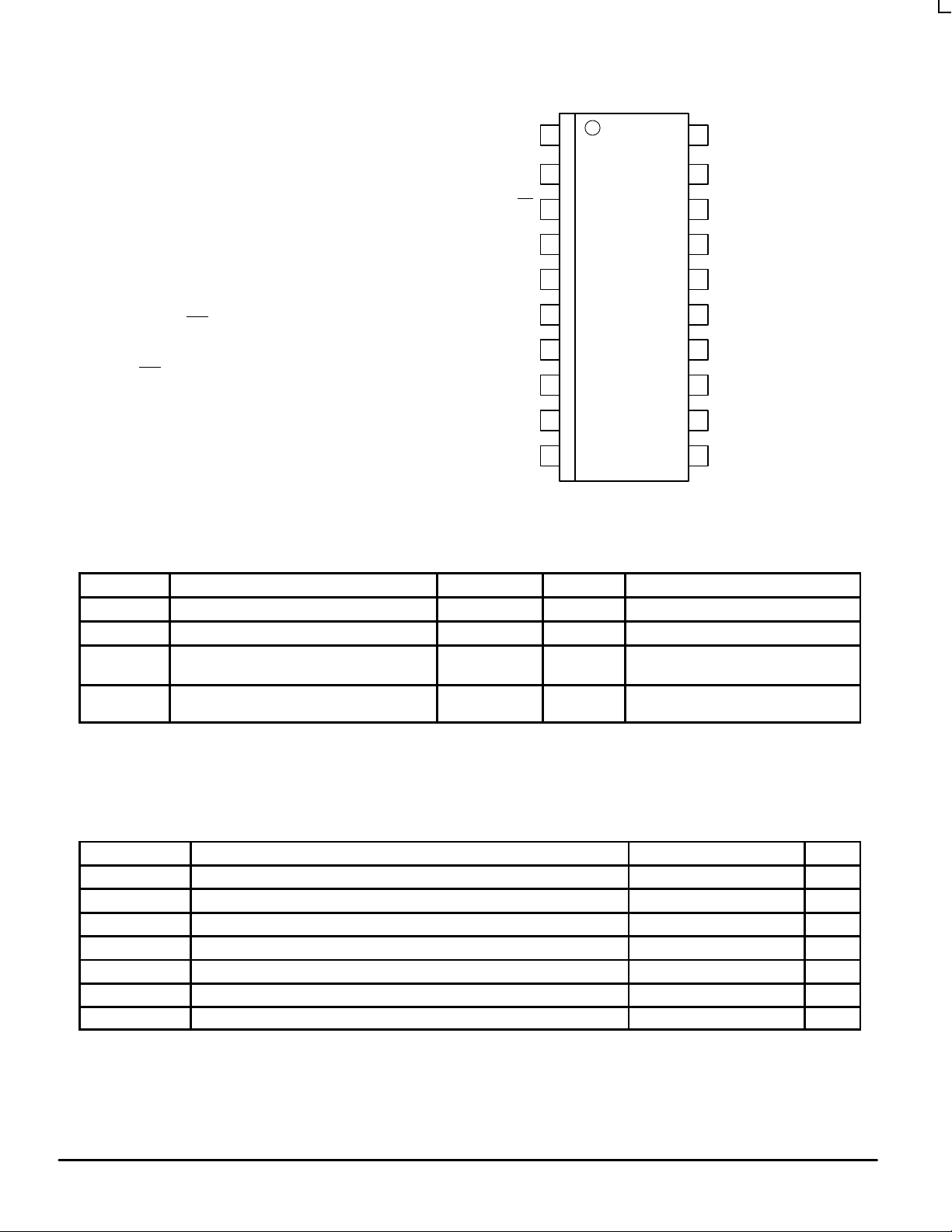
MC88921
20
19
18
GNDQ3
2X_QV
Q/2MR
Power–Down Mode Functionality
CC
1
2
3
The MC88921 has a special feature
designed in to allow the processor clock
PLL_EN
4
17
V
CC
inputs to be reset for total processor
power–down, and then to return to
5
16
Q2VCC(AN)
phase–locked operation very quickly when
the processor is powered–up again.
The MR
pin resets outputs 2X_Q, Q0
and Q1 only leaving the other outputs
6
7
15
14
GNDRC1
LOCKGND(AN)
operational for other system activity . When
MR
is negated, all outputs will be operating
normally within 3 clock cycles.
Q0
8
9
10
13
12
11
FBSELSYNC
Q1GND
V
CC
Pinout: 20–Lead Wide SOIC Package (Top View)
CAPACITANCE AND POWER SPECIFICATIONS
Symbol Parameter Value Typ Unit Test Conditions
C
C
PD
PD
IN
PD
1
2
Input Capacitance 4.5 pF VCC = 5.0V
Power Dissipation Capacitance 40 pF VCC = 5.0V
Power Dissipation at 33MHz With 50Ω
Thevenin Termination
Power Dissipation at 33MHz With 50Ω
Parallel Termination to GND
15mW/Output
90mW/Device
37.5mW/Output
225mW/Device
mW VCC = 5.0V
T = 25°C
mW VCC = 5.0V
T = 25°C
MAXIMUM RATINGS*
Symbol Parameter Limits Unit
VCC, AV
V
V
I
I
I
T
* Maximum Ratings are those values beyond which damage to the device may occur. Functional operation should be restricted to the
Recommended Operating Conditions.
MOTOROLA TIMING SOLUTIONS
CC
in
out
in
out
CC
stg
DC Supply Voltage Referenced to GND –0.5 to 7.0 V
DC Input Voltage (Referenced to GND) –0.5 to VCC +0.5 V
DC Output Voltage (Referenced to GND) –0.5 to VCC +0.5 V
DC Input Current, Per Pin ±20 mA
DC Output Sink/Source Current, Per Pin ±50 mA
DC VCC or GND Current Per Output Pin ±50 mA
Storage Temperature –65 to +150 °C
2
BR1333 — REV 5
MC88921
RECOMMENDED OPERATING CONDITIONS
Symbol Parameter Limits Unit
V
CC
V
in
V
out
T
A
ESD Static Discharge Voltage > 1500 V
DC CHARACTERISTICS (TA = –40°C to 85°C; VCC = 5.0V ± 5%)
Supply Voltage 5.0 ±10% V
DC Input Voltage 0 to V
DC Output Voltage 0 to V
Ambient Operating Temperature 0 to 70 °C
CC
CC
V
V
Symbol Parameter V
V
IH
V
IL
V
OH
V
OL
I
IN
I
CCT
I
OLD
I
OHD
I
CC
1. IOL is +12mA for the LOCK output.
2. The PLL_EN input pin is not guaranteed to meet this specification.
3. Maximum test duration 2.0ms, one output loaded at a time.
Minimum High Level Input Voltage 4.75
Minimum Low Level Input Voltage 4.75
Minimum High Level Output Voltage 4.75
Minimum Low Level Output Voltage 4.75
Maximum Input Leakage Current 5.25 ±1.0 µA VI = VCC, GND
Maximum ICC/Input 5.25 2.0
Minimum Dynamic3 Output Current 5.25 88 mA V
Maximum Quiescent Supply Current 5.25 750 µA VI = VCC, GND
CC
5.25
5.25
5.25
5.25
5.25 –88 mA V
Guaranteed Limits Unit Condition
2.0
2.0
0.8
0.8
4.01
4.51
0.44
0.44
2
V V
V V
V VIN = VIH or V
V VIN = VIH or V
mA VI = VCC – 2.1V
SYNC INPUT TIMING REQUIREMENTS
Symbol Parameter Minimum Maximum Unit
t
RISE/FALL
SYNC Input
t
,
CYCLE
SYNC Input
Duty Cycle Duty Cycle, SYNC Input 50% ± 25%
Rise/Fall Time, SYNC Input
From 0.8V to 2.0V
Input Clock Period
SYNC Input
— 5.0 ns
1
f
ń
4
2X_Q
= 0.1V or
OUT
VCC – 0.1V
= 0.1V or
OUT
VCC – 0.1V
I
OH –36mA
I
OH +36mA
OLD
OHD
–36mA
+36mA
= 1.0V Max
= 3.85 Min
200 ns
IL
IL
1
TIMING SOLUTIONS
BR1333 — REV 5
3 MOTOROLA
 Loading...