

Motorola MC88915TFN55, MC88915TFN100, MC88915TFN133, MC88915TFN160 Datasheet
SEMICONDUCTOR TECHNICAL DATA
"' '
" #&#$ %%
! ( #$"!$
The MC88915T Clock Driver utilizes phase–locked loop technology to
lock its low skew outputs’ frequency and phase onto an input reference
clock. It is designed to provide clock distribution for high performance
PC’s and workstations. For a 3.3V version, see the MC88LV915T data
sheet.
The PLL allows the high current, low skew outputs to lock onto a single
clock input and distribute it with essentially zero delay to multiple
components on a board. The PLL also allows the MC88915T to multiply a
low frequency input clock and distribute it locally at a higher (2X) system
frequency . Multiple 88915’ s can lock onto a single reference clock, which
is ideal for applications when a central system clock must be distributed
synchronously to multiple boards (see Figure 7).
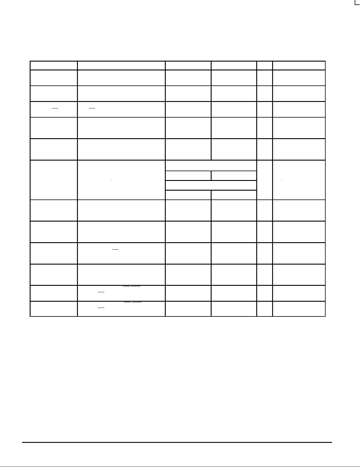
Five “Q” outputs (Q0–Q4) are provided with less than 500 ps skew between their rising edges. The Q5
phase shift) from the “Q” outputs. The 2X_Q output runs at twice the “Q” output frequency, while the Q/2 runs at 1/2 the “Q”
frequency.
The VCO is designed to run optimally between 20 MHz and the 2X_Q F
the different feedback configurations which create specific input/output frequency relationships. Possible frequency ratios of the
“Q” outputs to the SYNC input are 2:1, 1:1, and 1:2.
The FREQ_SEL pin provides one bit programmable divide–by in the feedback path of the PLL. It selects between divide–by–1
and divide–by–2 of the VCO before its signal reaches the internal clock distribution section of the chip (see the block diagram on
page 2). In most applications FREQ_SEL should be held high (÷1). If a low frequency reference clock input is used, holding
FREQ_SEL low (÷2) will allow the VCO to run in its optimal range (>20MHz and >40MHz for the TFN133 version).
In normal phase–locked operation the PLL_EN pin is held high. Pulling the PLL_EN pin low disables the VCO and puts the 88915
in a static “test mode”. In this mode there is no frequency limitation on the input clock, which is necessary for a low frequency board
test environment. The second SYNC input can be used as a test clock input to further simplify board–level testing (see detailed
description on page 1 1).
Pulling the OE
/RST pin goes back high Q0–Q4, Q5 and Q/2 will be reset in the low state, with 2X_Q being the inverse of the selected SYNC
OE
input. Assuming PLL_EN is low, the outputs will remain reset until the 88915 sees a SYNC input pulse.
A lock indicator output (LOCK) will go high when the loop is in steady–state phase and frequency lock. The LOCK output will go
low if phase–lock is lost or when the PLL_EN pin is low. The LOCK output will go high no later than 10ms after the 88915 sees a
SYNC signal and full 5V VCC.
/RST pin low puts the clock outputs 2X_Q, Q0–Q4, Q5 and Q/2 into a high impedance state (3–state). After the
max
LOW SKEW CMOS
PLL CLOCK DRIVER
output is inverted (180°
specification. The wiring diagrams in Figure 5 detail
Features
•
Five Outputs (Q0–Q4) with Output–Output Skew < 500 ps each being phase and frequency locked to the SYNC input
• The phase variation from part–to–part between the SYNC and FEEDBACK inputs is less than 550 ps (derived from the t
specification, which defines the part–to–part skew)
• Input/Output phase–locked frequency ratios of 1:2, 1:1, and 2:1 are available
• Input frequency range from 5MHz – 2X_Q FMAX spec. (10MHz – 2X_Q FMAX for the TFN133 version)
• Additional outputs available at 2X and +2 the system “Q” frequency. Also a Q (180° phase shift) output available
• All outputs have ±36 mA drive (equal high and low) at CMOS levels, and can drive either CMOS or TTL inputs. All inputs
are TTL–level compatible. ±88mA IOL/IOH specifications guarantee 50Ω transmission line switching on the incident edge
• Test Mode pin (PLL_EN) provided for low frequency testing. Two selectable CLOCK inputs for test or redundancy purposes.
All outputs can go into high impedance (3–state) for board test purposes
• Lock Indicator (LOCK) accuracy indicates a phase–locked state
Yield Surface Modeling and YSM are trademarks of Motorola, Inc.
1/97
Motorola, Inc. 1997
1
REV 4
PD
MC88915TFN55/70/100/133/160
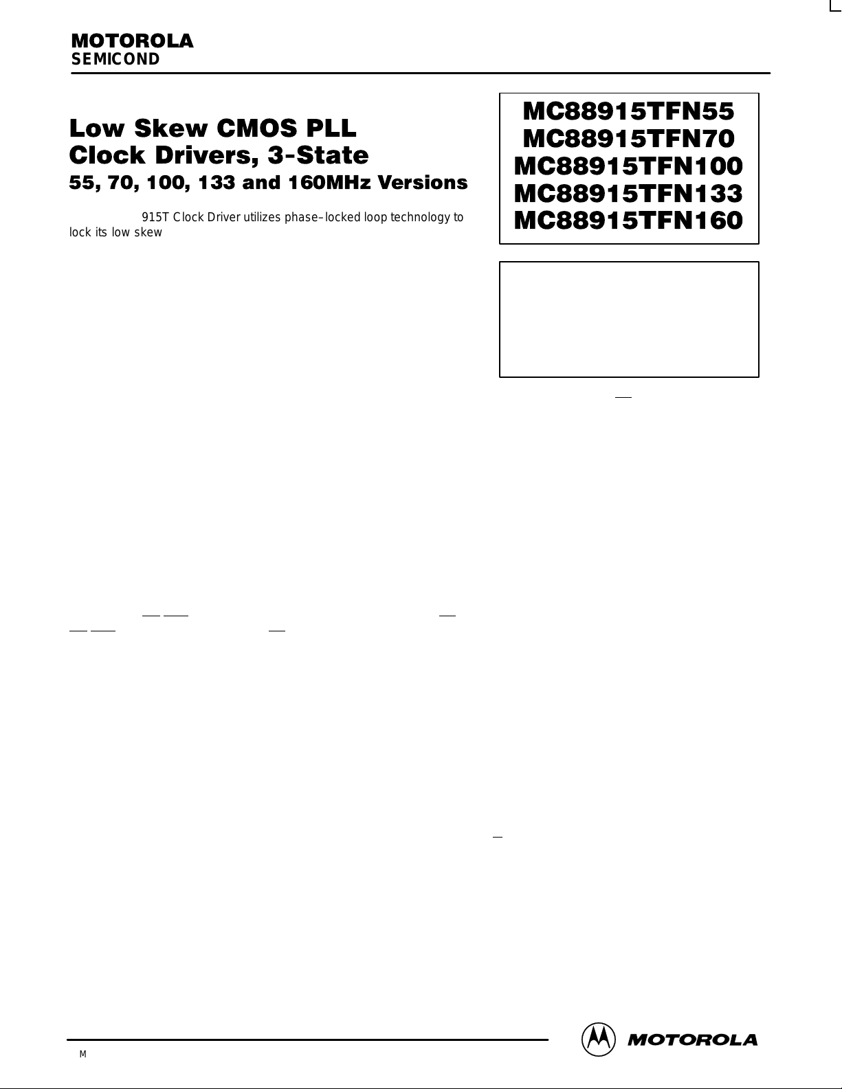
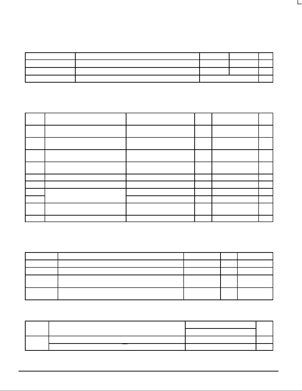
Pinout: 28–Lead PLCC (Top View)
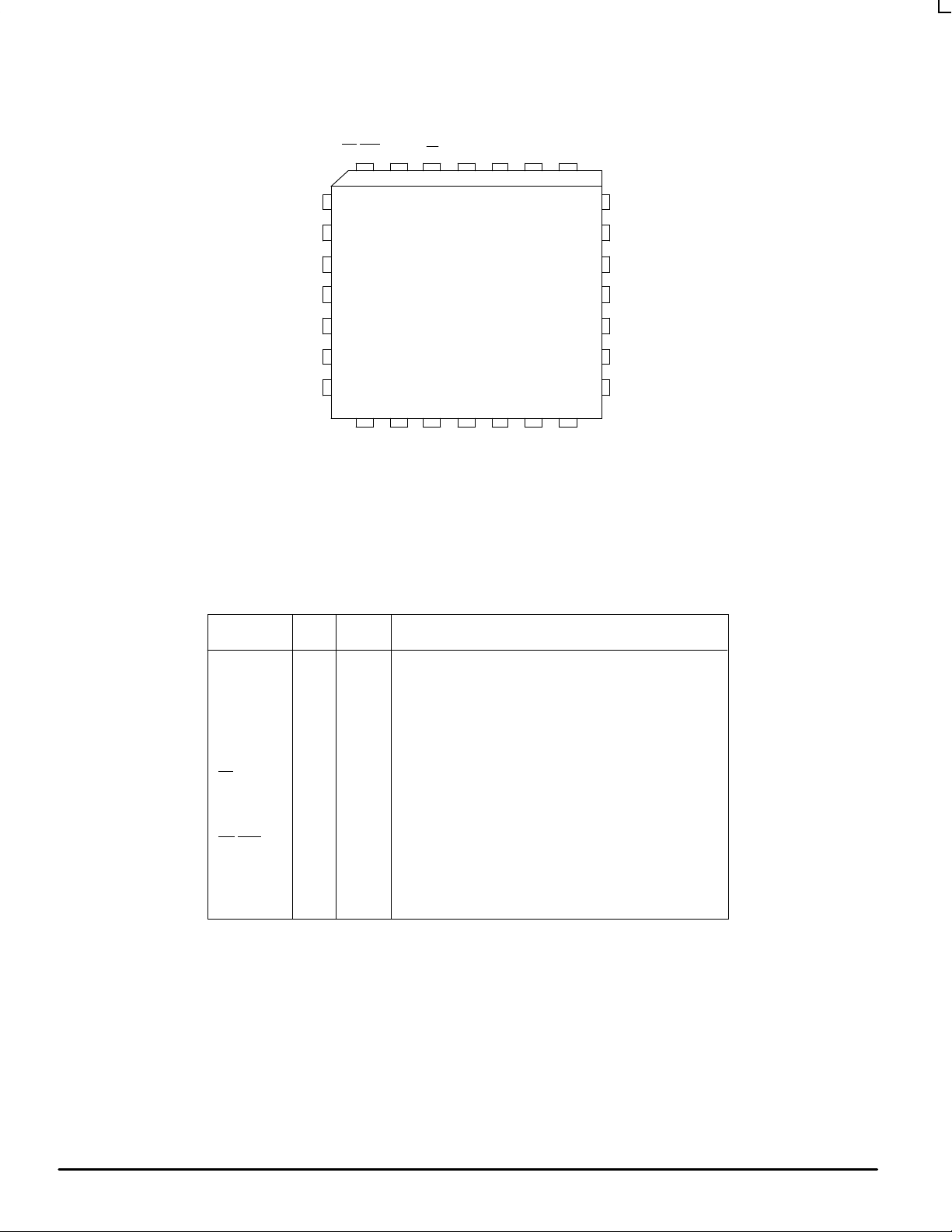
FEEDBACK
REF_SEL
SYNC[0]
VCC(AN)
RC1
GND(AN)
SYNC[1]
PIN SUMMARY
/RST V
5
6
7
8
9
10
FREQ_SEL
CC
Q0GND
FN SUFFIX
PLASTIC PLCC
CASE 776–02
CC
2X_QOE
V
Q4Q5 GND
CC
2627284321
Q/2
25
GND
24
Q3
23
V
22
CC
Q2
21
GND
20
LOCK
1911
18171612 13 14 15
PLL_ENGNDQ1V
Pin Name Num I/O Function
1
SYNC[0]
SYNC[1]
REF_SEL
FREQ_SEL
FEEDBACK
RC1
Q(0–4)
Q5
2x_Q
Q/2
LOCK
OE
/RST
PLL_EN
VCC,GND
11
Input
1
Input
1
Input
1
Input
1
Input
1
Input
5
Output
1
Output
1
Output
1
Output
1
Output
1
Input
1
Input
Reference clock input
Reference clock input
Chooses reference between sync[0] & Sync[1]
Doubles VCO Internal Frequency (low)
Feedback input to phase detector
Input for external RC network
Clock output (locked to sync)
Inverse of clock output
2 x clock output (Q) frequency (synchronous)
Clock output(Q) frequency
÷
2 (synchronous)
Indicates phase lock has been achieved (high when locked)
Output Enable/Asynchronous reset (active low)
Disables phase–lock for low freq. testing
Power and ground pins (note pins 8, 10 are
“analog” supply pins for internal PLL only)
MOTOROLA TIMING SOLUTIONS
2
BR1333 — Rev 6
FEEDBACK
MC88915TFN55/70/100/133/160
LOCK
SYNC (0)
SYNC (1)
REF_SEL
PLL_EN
FREQ_SEL
OE/RST
0
M
U
X
1
PHASE/FREQ.
DETECTOR
1
0
MUX
DIVIDE
BY TWO
CHARGE PUMP/LOOP
FILTER
EXTERNAL REC NETWORK
(RC1 Pin)
÷
1)
(
1
M
(
÷
2)
U
X
0
VOLTAGE
CONTROLLED
OSCILLA TOR
D
Q
CP
Q
R
D
Q
CP
R
D
Q
CP
R
2x_Q
Q0
Q1
Q2
MC88915T Block Diagram (All Versions)
D
CP
D
CP
D
CP
D
CP
Q
R
Q
R
Q
R
Q
R
Q3
Q4
Q5
Q/2
TIMING SOLUTIONS
BR1333 — Rev 6
3 MOTOROLA
MC88915TFN55/70/100/133/160
MC88915TFN55 and MC88915TFN70
SYNC INPUT TIMING REQUIREMENTS
Minimum
Symbol Parameter TFN70 TFN55 Maximum Unit
t
RISE/FALL
t
CYCLE
Duty Cycle SYNC Inputs Input Duty Cycle SYNC Inputs 50% ±25%
1. These t
in Figure 5b.
2. Information in Table 1 and in Note 3 of the AC specification notes describe this specification and its limits depending on what output is fed back,
and if FREQ_SEL is high or low.
DC ELECTRICAL CHARACTERISTICS
(Voltages Referenced to GND) TA =–40° C to +85° C for 55MHz Version; TA =0° C to +70° C for 70MHz Version; VCC = 5.0 V ± 5%
Symbol
V
V
V
OH
V
I
I
CCT
I
OLD
I
OHD
I
CC
I
OZ
1. IOL and IOH are 12mA and –12mA respectively for the LOCK output.
2. The PLL_EN input pin is not guaranteed to meet this specification.
3. Maximum test duration is 2.0ms, one output loaded at a time.
4. Specification value for IOZ is preliminary, will be finalized upon ‘MC’ status.
,SYNC Inputs Rise/Fall Time, SYNC Inputs
, SYNC Inputs Input Clock Period SYNC Inputs 28.5
minimum values are valid when ‘Q’ output is fed back and connected to the FEEDBACK pin. This is the configuration shown
CYCLE
Minimum High–Level Input
IH
Voltage
Maximum Low–Level Input
IL
Voltage
Minimum High–Level Output
Voltage
OL
Maximum Low–Level Output
Voltage
Maximum Input Leakage Current VI = VCC or GND 5.25 ±1.0 µA
in
Maximum ICC/Input VI = VCC – 2.1 V 5.25
Minimum Dynamic Output Current
Maximum Quiescent Supply
Current (per Package)
Maximum 3–State Leakage Current VI = VIH or VIL;VO = VCC or GND 5.25 ±50
From 0.8 to 2.0V
Parameter Test Conditions
V
= 0.1 V or VCC – 0.1 V 4.75
out
V
= 0.1 V or VCC – 0.1 V 4.75
out
Vin = VIH or V
IOH = –36 mA
Vin = VIH or V
IOL = 36 mA
3
V
OLD
V
OHD
VI = VCC or GND 5.25 1.0 mA
IL
1
IL
1
= 1.0V Max 5.25 88 mA
= 3.85V Min 5.25 –88 mA
— — 3.0 ns
V
CC
V
5.25
5.25
4.75
5.25
4.75
5.25
1
1
36.0
Target Limit Unit
2.0
2.0
0.8
0.8
4.01
4.51
0.44
0.44
2.0
200
2
4
2
ns
mA
µA
V
V
V
V
CAPACITANCE AND POWER SPECIFICATIONS
Symbol Parameter Typical Values Unit Conditions
C
IN
C
PD
PD
1
PD
2
NOTE: PD1 and PD2 mW/Output numbers are for a ‘Q’ output.
FREQUENCY SPECIFICATIONS (T
Symbol Parameter TFN70 TFN55 Unit
1
f
max
1. Maximum Operating Frequency is guaranteed with the part in a phase–locked condition, and all outputs loaded with 50Ω terminated to VCC/2.
MOTOROLA TIMING SOLUTIONS
Input Capacitance 4.5 pF VCC = 5.0 V
Power Dissipation Capacitance 40 pF VCC = 5.0 V
Power Dissipation @ 50MHz with 50Ω Thevenin Termination 23mW/Output
Power Dissipation @ 50MHz with 50Ω Parallel Termination to GND 57mW/Output
=–40° C to +85° C, VCC = 5.0 V ±5%)
A
Maximum Operating Frequency (2X_Q Output) 70 55 MHz
Maximum Operating Frequency (Q0–Q4,Q5 Output) 35 27.5 MHz
4
184mW/Device
456mW/Device
Guaranteed Minimum
mW VCC = 5.0 V
T = 25°C
mW VCC = 5.0 V
T = 25° C
BR1333 — Rev 6
MC88915TFN55/70/100/133/160
1,3
Cpu s)
pa a o
MC88915TFN55 and MC88915TFN70 (continued)
AC CHARACTERISTICS (T
Symbol
t
RISE/FALL
Outputs
t
RISE/FALL
2X_Q Output
t
PULSE WIDTH
(Q0–Q4, Q5
t
PULSE WIDTH
(2X_Q Output)
t
PULSE WIDTH
(2X_Q Output)
t
PD
SYNC Feedback (Measured at SYNC0 or 1 and
t
SKEWr
(Rising) See Note
t
SKEWf
(Falling)
t
SKEWall
t
LOCK
t
PZL
t
PHZ,tPLZ
1. These specifications are not tested, they are guaranteed by statistcal characterization. See AC specification Note 1.
2. T
CYCLE
3. The TPD specification’s min/max values may shift closer to zero if a larger pullup resistor is used.
4. Under equally loaded conditions and at a fixed temperature and voltage.
5. With VCC fully powered–on, and an output properly connected to the FEEDBACK pin. t
with C1 = 0.01µF.
6. The t
reached.
1
1
, Q/2)
1
1
1,4
1,4
1,4
5
6
PZL
5
6
in this spec is 1/Frequency at which the particular output is running.
, t
, t
PHZ
PLZ
=–40° C to +85° C, VCC = 5.0V ±5%, Load = 50Ω Terminated to VCC/2)
A
Parameter Min Max Unit Condition
Rise/Fall Time, All Outputs
(Between 0.2VCC and 0.8VCC)
Rise/Fall Time Into a 20pF Load, With
Termination Specified in Note
Output Pulse Width: Q0, Q1, Q2, Q3,
Q4, Q5
, Q/2 @ VCC/2
Output Pulse Width: 66MHz
2X_Q @ 1.5V 50MHz
Output Pulse Width: 50–65MHz
2X_Q @ VCC/2 40–49MHz
SYNC Input to Feedback Delay
FEEDBACK Input Pins)
Output–to–Output Skew Between Outputs Q0–Q4, Q/2 (Rising Edges Only)
Output–to–Output Skew Between Outputs Q0–Q4 (Falling Edges Only)
Output–to–Output Skew 2X_Q, Q/2,
Q0–Q4 Rising, Q5 Falling
Time Required to Acquire Phase–Lock
From Time SYNC Input Signal is
Received
Output Enable Time OE/RST to 2X_Q,
Q0–Q4, Q5
Output Disable Time OE/RST to 2X_Q,
Q0–Q4, Q5
minimum and maximum specifications are estimates, the final guaranteed values will be available when ‘MC’ status is
, and Q/2
, and Q/2
2
40MHz
66–70MHz
1.0 2.5 ns Into a 50Ω Load
0.5 1.6 ns t
0.5t
0.5t
0.5t
0.5t
0.5t
0.5t
0.5t
– 0.520.5t
CYCLE
– 0.5
CYCLE
CYCLE
(With 1MΩ from RC1 to An GND)
– 1.0
CYCLE
– 1.5
CYCLE
– 1.0
– 1.5
CYCLE
– 0.5
CYCLE
(With 1MΩ from RC1 to An VCC)
–1.05 –0.40
+1.25 +3.25
— 500 ps All Outputs Into a
— 500 ps All Outputs Into a
— 750 ps All Outputs Into a
1.0 10 ms Also Time to LOCK
3.0 14 ns Measured With the
3.0 14 ns Measured With the
CYCLE
2
0.5t
CYCLE
0.5t
CYCLE
0.5t
CYCLE
2
0.5t
CYCLE
0.5t
CYCLE
0.5t
CYCLE
maximum is with C1 = 0.1µF, t
LOCK
+ 0.5
+ 0.5
+ 1.0
+ 1.5
+ 1.0
+ 1.5
+ 0.5
2
ns Into a 50Ω Load
2
ns Must Use Termination
2
ns Into a 50Ω Load
ns See Note 4 and
Terminated to VCC/2
: 0.8V – 2.0V
RISE
t
: 2.0V – 0.8V
FALL
Terminated to VCC/2
Specified in Note 2
Terminated to VCC/2
Figure 2 for Detailed
Explanation
Matched 50Ω Load
Terminated to VCC/2
Matched 50Ω Load
Terminated to VCC/2
Matched 50Ω Load
Terminated to VCC/2
Indicator High
PLL_EN Pin Low
PLL_EN Pin Low
minimum is
LOCK
TIMING SOLUTIONS
BR1333 — Rev 6
5 MOTOROLA
MC88915TFN55/70/100/133/160
MC88915TFN100
SYNC INPUT TIMING REQUIREMENTS
Symbol Parameter Minimum Maximum Unit
t
RISE/FALL
t
CYCLE
Duty Cycle SYNC Inputs Input Duty Cycle SYNC Inputs 50% ±25%
1. These t
in Figure 5b.
2. Information in Table 1 and in Note 3 of the AC specification notes describe this specification and its limits depending on what output is fed back,
and if FREQ_SEL is high or low.
,SYNC Inputs Rise/Fall Time, SYNC Inputs From 0.8 to 2.0V — 3.0 ns
, SYNC Inputs Input Clock Period SYNC Inputs 20.0
minimum values are valid when ‘Q’ output is fed back and connected to the FEEDBACK pin. This is the configuration shown
CYCLE
1
200
2
ns
DC ELECTRICAL CHARACTERISTICS (Voltages Referenced to GND) T
Symbol
V
V
V
OH
V
OL
I
I
CCT
I
OLD
I
OHD
I
CC
I
OZ
1. IOL and IOH are 12mA and –12mA respectively for the LOCK output.
2. The PLL_EN input pin is not guaranteed to meet this specification.
3. Maximum test duration is 2.0ms, one output loaded at a time.
4. Specification value for IOZ is preliminary, will be finalized upon ‘MC’ status.
Minimum High–Level Input
IH
Voltage
Maximum Low–Level Input
IL
Voltage
Minimum High–Level Output
Voltage
Maximum Low–Level Output
Voltage
Maximum Input Leakage Current VI = VCC or GND 5.25 ±1.0 µA
in
Maximum ICC/Input VI = VCC – 2.1 V 5.25
Minimum Dynamic Output Current
Maximum Quiescent Supply
Current (per Package)
Maximum 3–State Leakage Current VI = VIH or VIL;VO = VCC or GND 5.25 ±50
Parameter Test Conditions
V
= 0.1 V or VCC – 0.1 V 4.75
out
V
= 0.1 V or VCC – 0.1 V 4.75
out
Vin = VIH or V
IOH = –36 mA
Vin = VIH or V
IOL = 36 mA
3
V
= 1.0V Max 5.25 88 mA
OLD
V
= 3.85V Min 5.25 –88 mA
OHD
VI = VCC or GND 5.25 1.0 mA
=–40° C to +85° C, VCC = 5.0 V ± 5%
A
V
CC
V
5.25
5.25
IL
1
IL
1
4.75
5.25
4.75
5.25
Target Limit Unit
2.0
2.0
0.8
0.8
4.01
4.51
0.44
0.44
2
2.0
4
CAPACITANCE AND POWER SPECIFICATIONS
Symbol Parameter Typical Values Unit Conditions
C
IN
C
PD
PD
1
PD
2
NOTE: PD1 and PD2 mW/Output numbers are for a ‘Q’ output.
Input Capacitance 4.5 pF VCC = 5.0 V
Power Dissipation Capacitance 40 pF VCC = 5.0 V
Power Dissipation @ 50MHz with 50Ω Thevenin Termination 23mW/Output
184mW/Device
Power Dissipation @ 50MHz with 50Ω Parallel Termination to GND 57mW/Output
456mW/Device
mW VCC = 5.0 V
mW VCC = 5.0 V
V
V
V
V
mA
µA
T = 25°C
T = 25° C
FREQUENCY SPECIFICATIONS (T
Symbol Parameter TFN100 Unit
1
f
max
1. Maximum Operating Frequency is guaranteed with the part in a phase–locked condition, and all outputs loaded with 50Ω terminated to VCC/2.
MOTOROLA TIMING SOLUTIONS
Maximum Operating Frequency (2X_Q Output) 100 MHz
Maximum Operating Frequency (Q0–Q4,Q5 Output) 50 MHz
=–40° C to +85° C, VCC = 5.0 V ±5%)
A
6
Guaranteed Minimum
BR1333 — Rev 6
 Loading...