

Motorola MC88914D, MC88914N Datasheet
SEMICONDUCTOR TECHNICAL DATA
The MC88914 is a high–speed, low power, hex divide–by–two D–type
flip–flop with matched propagation delays, an internal power–on–reset,
and external synchronous reset. With TTL compatible buffered clock and
external reset inputs that are common to all flip–flops, the MC88914 is
ideal for use in high–frequency systems as a clock driver, providing
multiple outputs that are synchronous.
• Power–on–Reset and External Synchronous Reset
• TTL Compatible Positive Edge–Triggered Clock
• Matched Outputs for Synchronous Applications
• Outputs Source/Sink 24mA
• Part–to–Part Skew of Less Than 3.0ns
• Guaranteed Rise and Fall Times for a Given Capacitive Load
Pinout: 14–Lead Plastic (Top View)
V
GND
Q
Q
Q
SR
GND
9
8
14
CC
13
12
5
4
3
11
10
Order this document
from Logic Marketing
LOW SKEW CMOS
CLOCK DRIVER
WITH RESET
14
1
N SUFFIX
PLASTIC PACKAGE
CASE 646–06
SR
POWER–ON
CLK
RESET
14
1
D SUFFIX
1
2
3
4
5
6
7
V
GND
Q
Q
Q
CLK
CC
0
1
2
GND
PLASTIC PACKAGE
CASE 751A–03
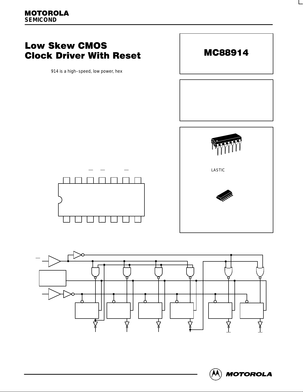
LOGIC DIAGRAM
CLK D
RST
Q
Q
CLK D
RST RST RST RST RST
Q
0
Q
CLK D
Q
1
Q
CLK D
Q
2
Q
3
CLK D
CLK D
Q
Q
4
Q
Q
5
8/95
Motorola, Inc. 1995
NOTE: This diagram is provided only for understanding of logic operation and should not be used to estimate propagation delays
1
REV 4

MC88914
DC CHARACTERISTICS (unless otherwise specified)
Symbol
I
CC
I
CC
I
CCT
Maximum Quiescent Supply Current 80 µA VIN = VCC or GND
Maximum Quiescent Supply Current 8.0 µA VIN = VCC or GND
Maximum Additional ICC/Input 1.5 mA VIN = VCC –2.1V
DC CHARACTERISTICS
Symbol Parameter V
V
IH
V
IL
V
OH
V
OL
I
IN
I
CCT
I
OLD
I
OHD
* All outputs loaded; thresholds on inputs associated with output under test.
** Maximum test duration 20ms, one output at a time.
Minimum High Level
Input Voltage
Maximum Low Level
Input Voltage
Minimum High Level 4.5
Maximum Low Level
Output Voltage
Maximum Input 5.5 ±0.1 ±0.1 µA VI = VCC, GND
Maximum ICC/Input 5.5 0.6 1.5 mA VI = VCC –2.1V
Minimum Dynamic Output Current** 5.5 75 mA V
Parameter Unit Condition
TA = +25°C
CC
4.5
5.5
4.5
5.5
5.5
4.5
5.5
4.5
5.5
4.5
5.5
5.5 –75 mA V
Typ Guaranteed Max Unit Conditions
1.5
1.5
1.5
1.5
4.49
5.49
0.001
0.001
2.0
2.0
0.8
0.8
4.4
5.4
3.86
4.86
0.1
0.1
0.36
0.36
TA =
–40 to +85°C
2.0
2.0
0.8
0.8
4.4
5.4
3.76
4.76
0.1
0.1
0.44
0.44
VCC = 5.5V,
TA = Worst Case
VCC = 5.5V,
TA = 25°C
VCC = 5.5V,
TA = Worst Case
V V
V V
V I
V *VIN = VIL or V
V I
V *VIN = VIL or V
= 0.1V or
OUT
VCC – 0.1V
= 0.1V or
OUT
VCC – 0.1V
= –50µA
OUT
IOH = –24mA
–24mA
= 50µA
OUT
IOH = 24mA
24mA
= 1.65V
OLD
= 3.85V
OHD
IH
IH
MOTOROLA TIMING SOLUTIONS
2
BR1333 — REV 5
 Loading...