

Motorola MC88913D, MC88913N Datasheet
SEMICONDUCTOR TECHNICAL DATA
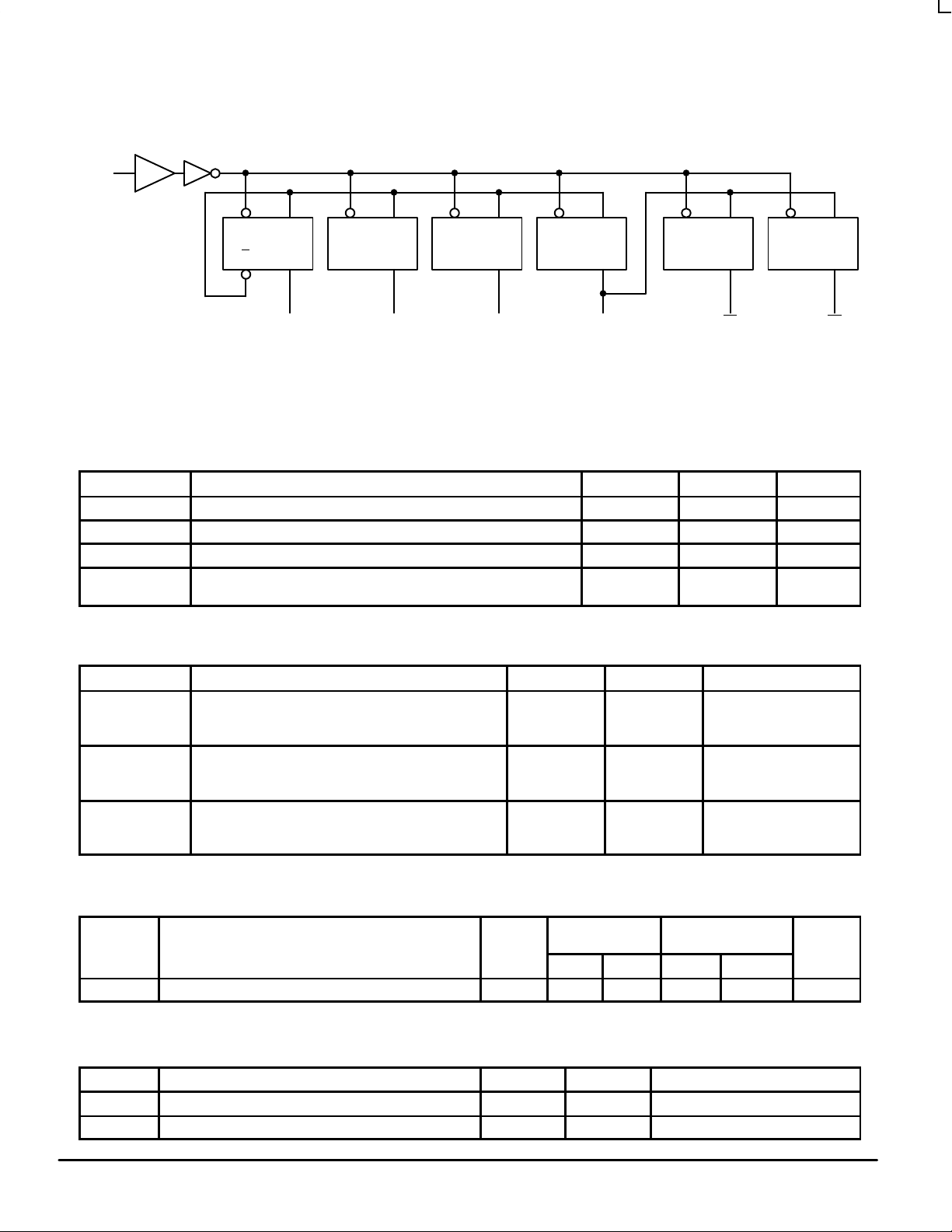
The MC88913 is a high–speed, low power, hex divide–by–two D–type
flip–flop with two inverting and four non–inverting outputs that have
closely matched propagation delays. With a TTL compatible buffered
clock input that is common to all flip–flops, the MC88913 is ideal for use in
high–frequency systems as a clock driver, providing multiple outputs that
are synchronous.
Order this document
from Logic Marketing
LOW SKEW CMOS
CLOCK DRIVER
• Minimum Clock Input f
MAX
of 1 10MHz
• TTL Compatible Positive Edge–Triggered Clock
• Matched Outputs for Synchronous Applications
• Outputs Source/Sink 24mA
• Part–to–Part Skew of Less Than 4.0ns
• Guaranteed Rise and Fall Times for a Given Capacitive Load
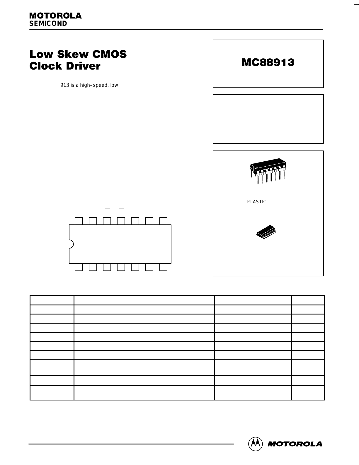
Pinout: 14–Lead Plastic (Top View)
V
GND
Q
Q
Q
GND
9
6
GND
GND
8
7
GND
SOIC Package**
5
12
Q
4
3
11
10
3
4
5
Q
0
Q
1
2
CC
14
1
GND
13
2
CLK
MAXIMUM RATINGS*
Symbol
V
CC
V
in
V
out
I
in
I
out
I
CC
P
D
T
stg
T
L
* Maximum Ratings are those values beyond which damage to the device may occur. Functional operation should be restricted to the
Recommended Operating Conditions.
** Derating: Plastic Package: –10mW/°C from 65°C to 125°C
DC Supply Voltage (Referenced to GND) –0.5 to +7.0 V
DC Input Voltage (Referenced to GND) –0.5 to VCC + 0.5 V
DC Output Voltage (Referenced to GND) –0.5 to VCC + 0.5 V
DC Input Current, per Pin ± 20 mA
DC Output Sink/Source Current, per Pin ± 50 mA
DC VCC or GND Current per Output Pin ± 50 mA
Power Dissipation in Still Air Plastic Package**
Storage Temperature –65 to +150 °C
Lead Temperature, 1mm from Case for 10s (Plastic or SOIC
Package)
SOIC Package: –7.0mW/°C from 65°C to 125°C
Parameter Value Units
14
1
N SUFFIX
PLASTIC PACKAGE
CASE 646–06
14
1
D SUFFIX
PLASTIC PACKAGE
CASE 751A–03
750
500
260 °C
mW
11/93
Motorola, Inc. 1995
1
REV 3
MC88913
CLK
LOGIC DIAGRAM
CLKQD
Q
Q
0
NOTE: This diagram is provided only for understanding of logic operation and should not be used to estimate propagation delays
CLK D
Q
Q
1
RECOMMENDED OPERATING CONDITIONS
Parameter Min Max Unit
V
meas
V
CC
Vin, V
T
A
tr, t
f
Symbol
out
DC Supply Voltage (Referenced to GND) 2.0 6.0 V
DC Input Voltage, Output Voltage (Referenced to GND) 0 V
Operating Temperature –40 +85 °C
Input Rise and Fall Time Vin from 0.8 to 2.0V
DC CHARACTERISTICS (unless otherwise specified)
Parameter Unit Condition
I
CC
I
CC
I
CCT
Symbol
Maximum Quiescent Supply Current 80 µA VIN = VCC or GND
Maximum Quiescent Supply Current 8.0 µA VIN = VCC or GND
Maximum Additional ICC/Input 1.5 mA VIN = VCC –2.1V
CLK D
from 0.8 to 2.0V
CLK D
Q
Q
2
Q
Q
3
0
0
CLK D
8.0
VCC = 5.5V,
TA = Worst Case
VCC = 5.5V,
TA = 25°C
VCC = 5.5V,
TA = Worst Case
Q
Q
CC
10
CLK D
Q
V
ns/V
Q
5
4
AC OPERATING REQUIREMENTS
TA = 25°C
CL = 50 pF
Symbol Parameter VCC (V) Min Max Min Max Unit
t
W
CLK Pulse Width (HIGH to LOW) 5.0 3.0 3.0 ns
TA = –40 to +85°C
CL = 50 pF
CAPACITANCE
Symbol
C
IN
C
PD
MOTOROLA TIMING SOLUTIONS
Input Capacitance 4.5 pF VCC = 5.0V
Power Dissipation Capacitance 30 pF VCC = 5.0V
Parameter Typ Unit Condition
2
BR1333 — REV 5
 Loading...