

Motorola MC78FC30HT1, MC78FC33HT1, MC78FC40HT1, MC78FC50HT1 Datasheet
T
30° to +80°C
SOT–89
Order this document by MC78FC00/D
The MC78FC00 series voltage regulators are specifically designed for
use as a power source for video instruments, handheld communication
equipment, and battery powered equipment.
The MC78FC00 series voltage regulator ICs feature a high accuracy
output voltage and ultra–low quiescent current. Each device contains a
voltage reference unit, an error amplifier, a driver transistor, and resistors for
setting output voltage, and a current limit circuit. These devices are available
in SOT–89 surface mount packages, and allow construction of an efficient,
constant voltage power supply circuit.
MC78FC00 Series Features:
• Ultra–Low Quiescent Current of 1.1 µA Typical
• Ultra–Low Dropout Voltage (100 mV at 10 mA)
• Large Output Current (up to 120 mA)
• Excellent Line Regulation (0.1%)
• Wide Operating Voltage Range (2.0 V to 10 V)
• High Accuracy Output Voltage (±2.5%)
• Wide Output Voltage Range (2.0 V to 6.0 V)
• Surface Mount Package (SOT–89)
ORDERING INFORMATION
Output
Device
MC78FC30HT1 3.0
MC78FC33HT1 3.3
MC78FC40HT1 4.0
MC78FC50HT1 5.0
Other voltages from 2.0 to 6.0 V, in 0.1 V increments, are available upon request. Consult
factory for information.
Voltage
Operating
Temperature Range
–
°
A
= –
°
Package
–
MICROPOWER ULTRA–LOW
QUIESCENT CURRENT
VOLTAGE REGULATORS
SEMICONDUCTOR
TECHNICAL DATA
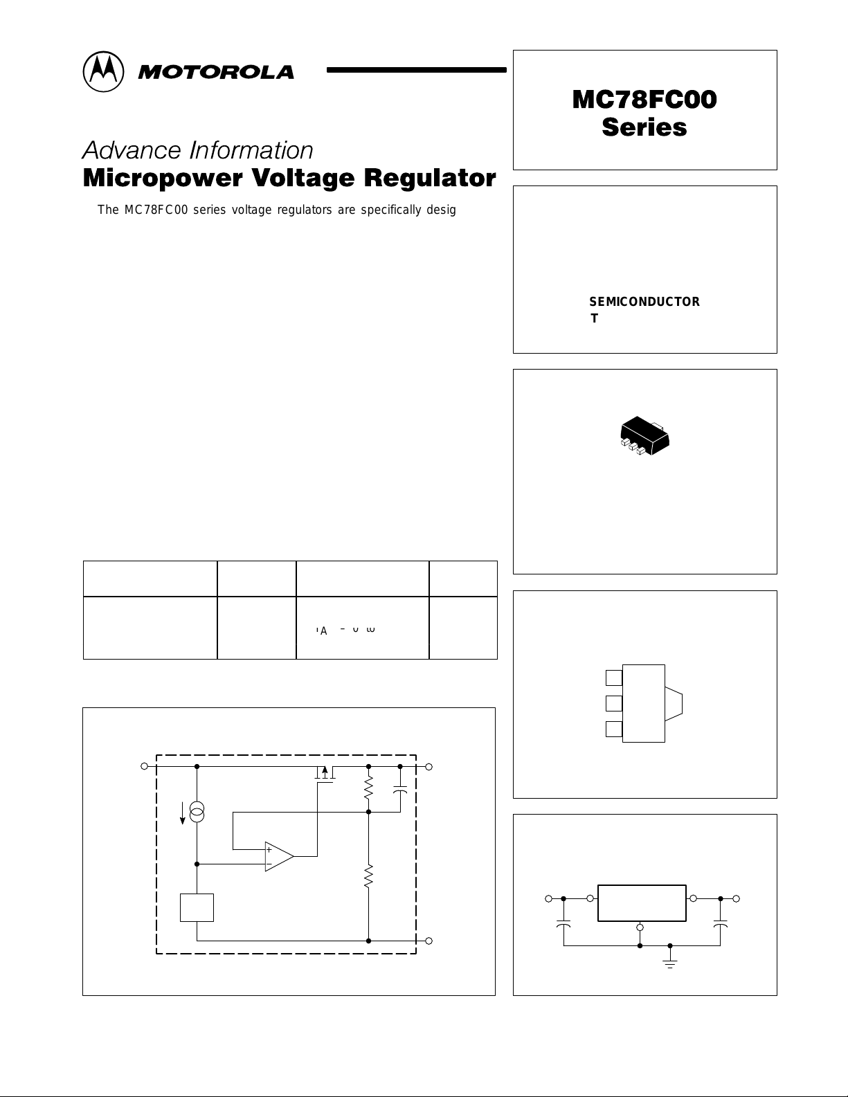
TAB
1
H SUFFIX
PLASTIC PACKAGE
CASE 1213
(SOT–89)
PIN CONNECTIONS
1
Ground
Representative Block Diagram
2
V
in
V
ref
This device contains 11 active transistors.
This document contains information on a new product. Specifications and information herein
are subject to change without notice.
MOTOROLA ANALOG IC DEVICE DATA
2
Input
3
Output
3
V
O
(Top View)
Tab
(Tab is connected
to Pin 2)
Standard Application
Input Output
1
Gnd
Motorola, Inc. 1996 Rev 0
C
in
2
MC78FCXX
1
3
C
O
1
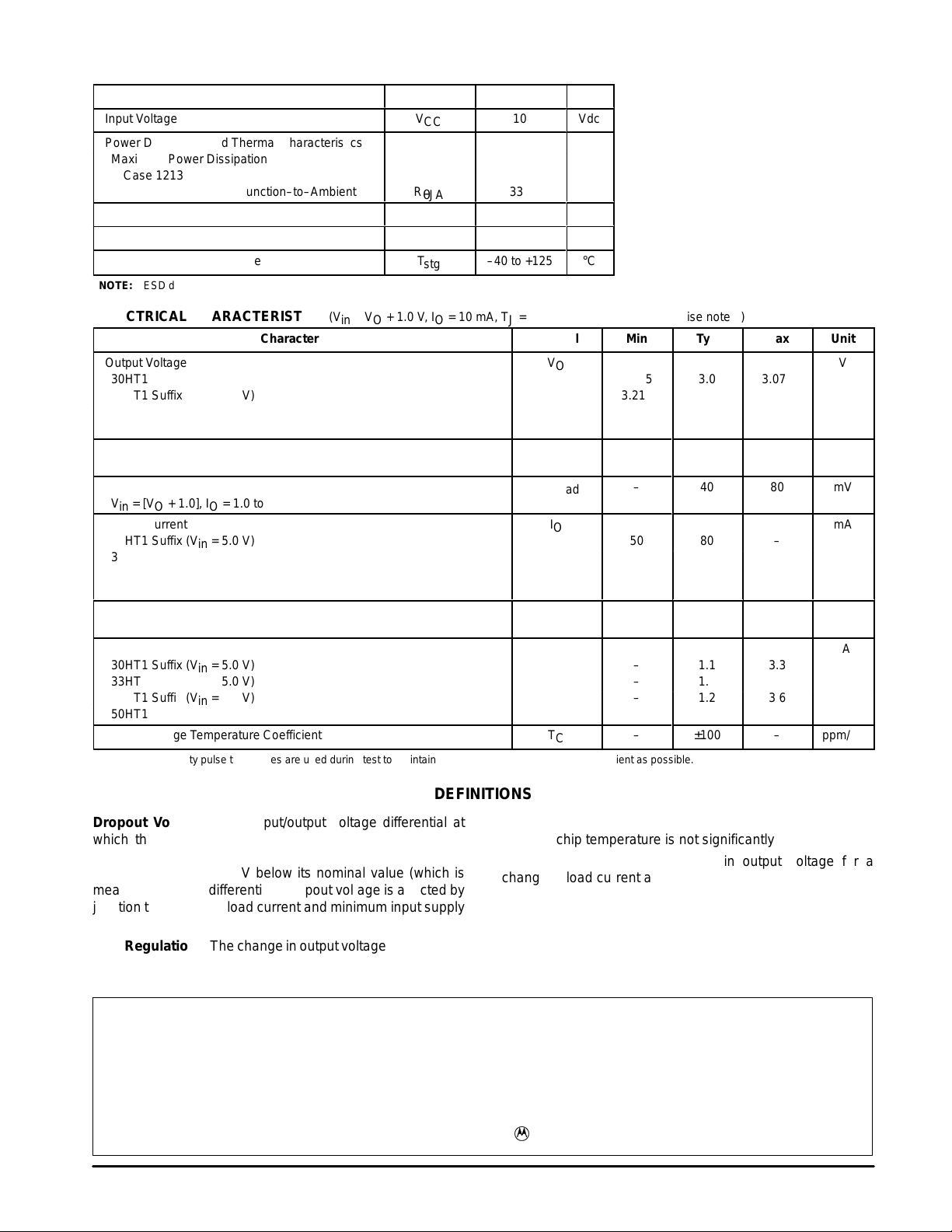
MAXIMUM RATINGS
ÁÁÁ
ÁÁÁ
ÁÁÁ
ÁÁÁ
ÁÁÁ
ÁÁÁ
ÁÁÁ
(TC = 25°C, unless otherwise noted.)
Rating Symbol Value Unit
Input Voltage
Power Dissipation and Thermal Characteristics
Maximum Power Dissipation
Case 1213 (SOT–89) H Suffix P
Thermal Resistance, Junction–to–Ambient R
Operating Junction Temperature
Operating Ambient Temperature
Storage Temperature Range
NOTE: ESD data available upon request.
MC78FC00 Series
V
T
CC
D
θJA
T
T
A
stg
J
10
300 mW
333 °C/W
125
–30 to +80
–40 to +125
Vdc
°C
°C
°C
ELECTRICAL CHARACTERISTICS (V
Characteristic
Output Voltage
= VO + 1.0 V, IO = 10 mA, TJ = 25°C [Note 1], unless otherwise noted.)
in
Symbol Min Typ Max Unit
V
O
30HT1 Suffix (Vin = 5.0 V) 2.925 3.0 3.075
33HT1 Suffix (Vin = 6.0 V) 3.218 3.3 3.382
40HT1 Suffix (Vin = 7.0 V) 3.900 4.0 4.100
50HT1 Suffix (Vin = 8.0 V) 4.875 5.0 5.125
Line Regulation
Reg
line
–
0.1
Vin = [VO + 1.0] V to 10 V, IO = 10 mA
Load Regulation
Reg
load
–
40
Vin = [VO + 1.0], IO = 1.0 to 10 mA
Output Current
I
O
30HT1 Suffix (Vin = 5.0 V) 50 80 –
33HT1 Suffix (Vin = 6.0 V) 65 100 –
40HT1 Suffix (Vin = 7.0 V) 65 100 –
50HT1 Suffix (Vin = 8.0 V) 80 120 –
Dropout Voltage
Vin – V
O
–
0.5
IO = 40 mA
Quiescent Current
I
CC
30HT1 Suffix (Vin = 5.0 V) – 1.1 3.3
33HT1 Suffix (Vin = 5.0 V) – 1.1 3.3
40HT1 Suffix (Vin = 6.0 V) – 1.2 3.6
50HT1 Suffix (Vin = 7.0 V) – 1.3 3.9
Output Voltage Temperature Coefficient
NOTE: 1.Low duty pulse techniques are used during test to maintain junction temperature as close to ambient as possible.
T
C
–
±100
80
0.7
V
–
mV
mV
mA
V
µA
–
ppm/°C
DEFINITIONS
Dropout Voltage – The input/output voltage differential at
which the regulator output no longer maintains regulation
against further reductions in input voltage. Measured when
the output drops 100 mV below its nominal value (which is
measured at 1.0 V differential), dropout voltage is affected by
junction temperature, load current and minimum input supply
requirements.
Line Regulation – The change in output voltage for a change
in input voltage. The measurement is made under conditions
Motorola reserves the right to make changes without further notice to any products herein. Motorola makes no warranty , representation or guarantee regarding
the suitability of its products for any particular purpose, nor does Motorola assume any liability arising out of the application or use of any product or circuit, and
specifically disclaims any and all liability, including without limitation consequential or incidental damages. “T ypical” parameters which may be provided in Motorola
data sheets and/or specifications can and do vary in different applications and actual performance may vary over time. All operating parameters, including “Typicals”
must be validated for each customer application by customer’s technical experts. Motorola does not convey any license under its patent rights nor the rights of
others. Motorola products are not designed, intended, or authorized for use as components in systems intended for surgical implant into the body, or other
applications intended to support or sustain life, or for any other application in which the failure of the Motorola product could create a situation where personal injury
or death may occur. Should Buyer purchase or use Motorola products for any such unintended or unauthorized application, Buyer shall indemnify and hold Motorola
and its officers, employees, subsidiaries, affiliates, and distributors harmless against all claims, costs, damages, and expenses, and reasonable attorney fees
arising out of, directly or indirectly, any claim of personal injury or death associated with such unintended or unauthorized use, even if such claim alleges that
Motorola was negligent regarding the design or manufacture of the part. Motorola and are registered trademarks of Motorola, Inc. Motorola, Inc. is an Equal
Opportunity/Affirmative Action Employer.
2
of low dissipation or by using pulse techniques such that
average chip temperature is not significantly affected.
Load Regulation – The change in output voltage for a
change in load current at constant chip temperature.
Maximum Power Dissipation – The maximum total device
dissipation for which the regulator will operate within
specifications.
Quiescent Bias Current – Current which is used to operate
the regulator chip and is not delivered to the load.
MOTOROLA ANALOG IC DEVICE DATA
 Loading...