

MOTOROLA MC75174BP, MC75174BDW, MC75172BDWR2, MC75174BDWR2 Datasheet
Order this document by MC75172B/D
!
The Motorola MC75172B/174B Quad Line drivers are differential high
speed drivers designed to comply with the EIA–485 Standard. Features
include three–state outputs, thermal shutdown, and output current limiting in
both directions. These devices also comply with EIA–422–A, and CCITT
Recommendations V.11 and X.27.
The MC75172B/174B are optimized for balanced multipoint bus
transmission at rates in excess of 10 MBPS. The outputs feature wide
common mode voltage range, making them suitable for party line
applications in noisy environments. The current limit and thermal shutdown
features protect the devices from line fault conditions. These devices offer
optimum performance when used with the MC75173 and MC75175 line
receivers.
Both devices are available in 16–pin plastic DIP and 20–pin wide body
surface mount packages.
• Meets EIA–485 Standard for Party Line Operation
• Meets EIA–422–A and CCITT Recommendations V.11 and X.27
• Operating Ambient Temperature: –40°C to +85°C
• High Impedance Outputs
• Common Mode Output Voltage Range: –7 to 12 V
• Positive and Negative Current Limiting
• Transmission Rates in Excess of 10 MBPS
• Thermal Shutdown at 150°C Junction Temperature, (±
• Single 5.0 V Supply
• Pin Compatible with TI SN75172/4 and NS µA96172/4
• Interchangeable with MC3487 and AM26LS31 for EIA–422–A
Applications
ā
20°C)
QUAD EIA–485 LINE DRIVERS
SEMICONDUCTOR
TECHNICAL DATA
P SUFFIX
PLASTIC PACKAGE
CASE 648
DW SUFFIX
PLASTIC PACKAGE
CASE 751D
(SO–20L)
ORDERING INFORMATION
Operating
Device
MC75172BDW
MC75174BDW SO–20L
MC75174BP Plastic DIP
Temperature Range
TA = –40° to +85°C
Package
SO–20L
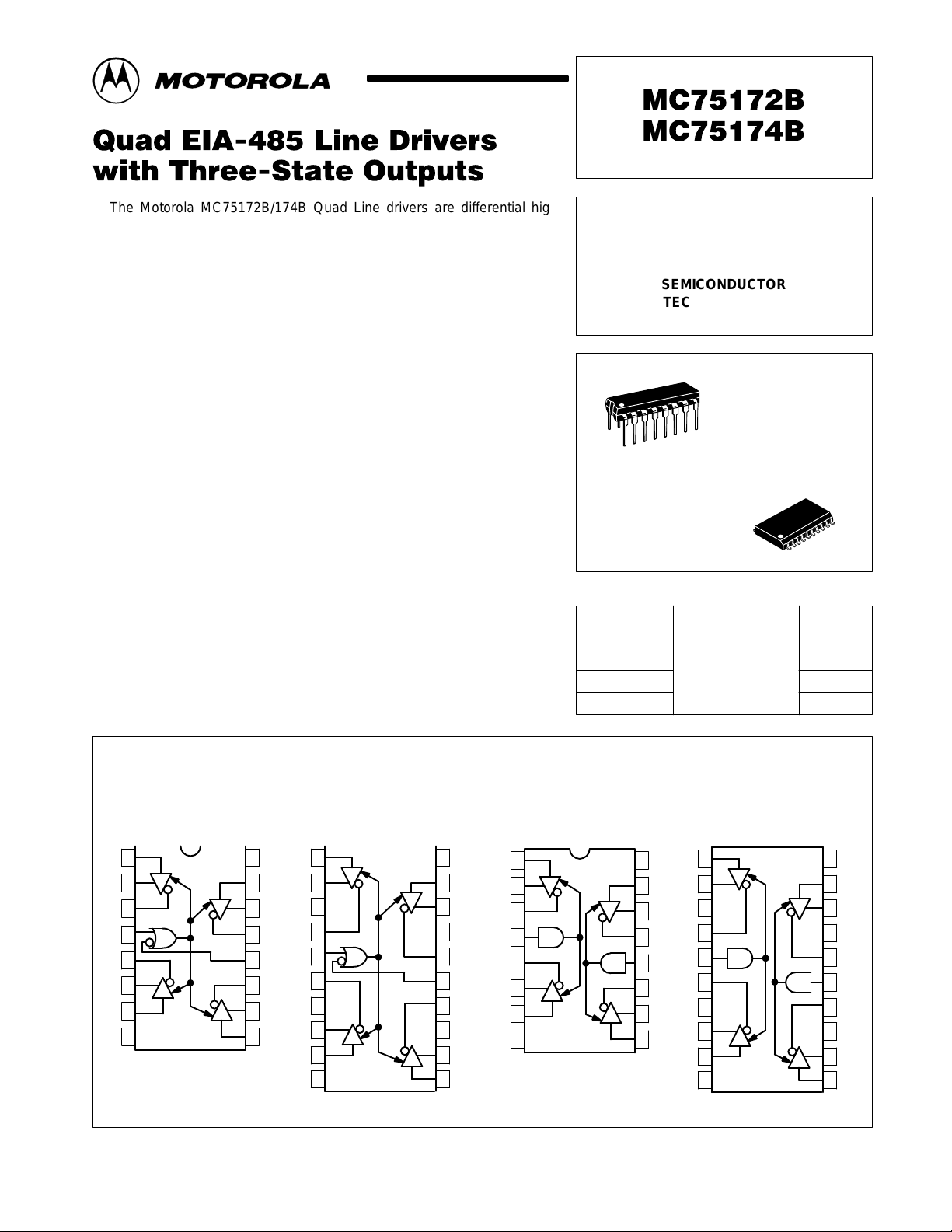
MC75172B MC75174B
1A
1Y
1Z
En
2Z
2Y
2A
Gnd
1
2
3
4
5
6
7
8
P Package
16
15
14
13
12
11
10
V
4A
4Y
4Z
En
3Z
3Y
9
3A
MOTOROLA ANALOG IC DEVICE DATA
1
1A
CC
2
1Y
3
NC
4
1Z NC
5
En
6
2Z
7
NC
8
2Y
9
2A
10 11
Gnd
DW Package
PIN CONNECTIONS
20
19
18
17
16
15
14
13
12
V
4A
4Y
4Z
En
3Z
NC
3Y
3A
CC
1A
1Y
1Z
En
12
2Z
2Y
2A
Gnd
1
2
3
4
5
6
7
8
1
1A
16
V
CC
2
1Y
15
4A
3
NC
14
4Y
4
1Z
13
4Z
En
5
En
12
12
34
2Z
11
10
9
P Package
Motorola, Inc. 1996 Rev 1
6
3Z
7
NC
3Y
2Y
8
3A
9
2A
10 11
Gnd
DW Package
20
19
18
17
16
15
14
13
12
V
4A
4Y
NC
4Z
En
34
3Z
NC
3Y
3A
CC
1
MC75172B MC75174B
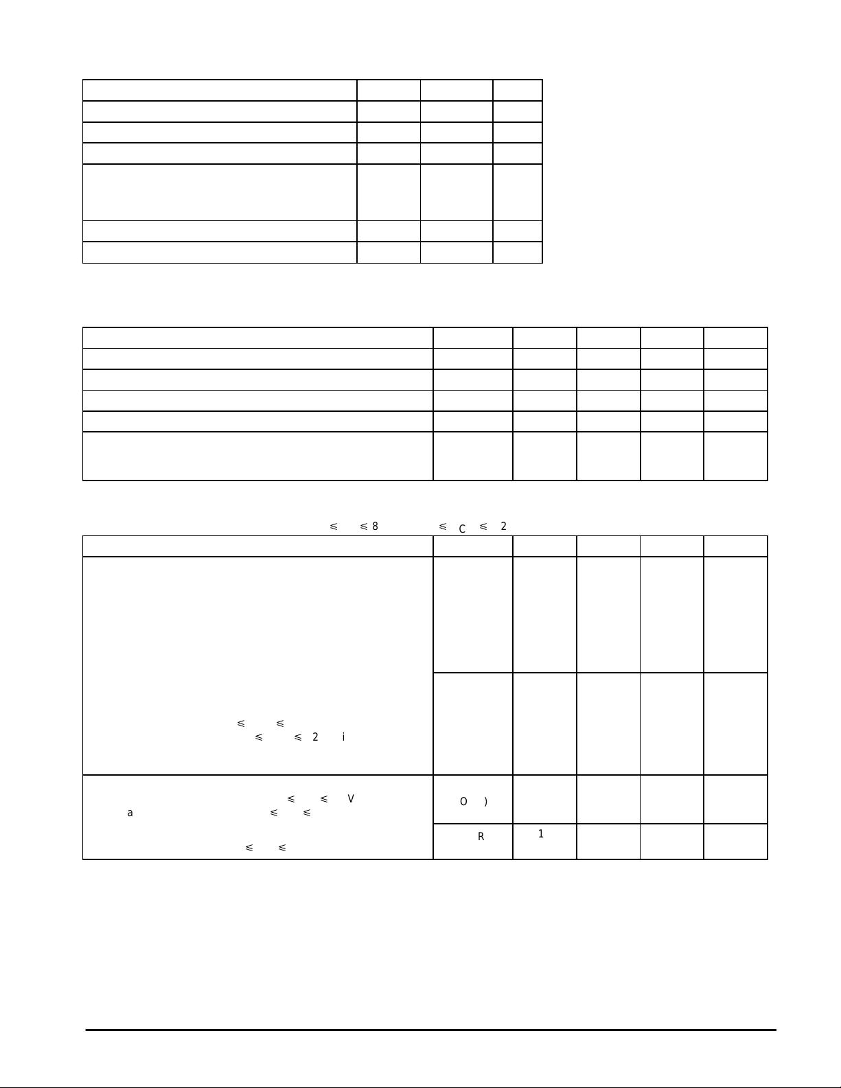
MAXIMUM RATINGS
Rating Symbol Value Unit
Power Supply Voltage V
Input Voltage (Data, Enable) V
Input Current (Data, Enable) I
Applied Output Voltage, when in 3–State Condition
(VCC = 5.0 V)
Applied Output Voltage, when VCC = 0 V V
Output Current I
Storage Temperature T
Devices should not be operated at these limits. The “Recommended Operating Conditions” table provides
for actual device operation.
CC
in
in
V
za
zb
O
stg
RECOMMENDED OPERATING CONDITIONS
Characteristic Symbol Min Typ Max Unit
Power Supply Voltage V
Input Voltage (All Inputs) V
Output Voltage in 3–State Condition, or when VCC = 0 V V
Output Current (Normal data transmission) I
Operating Ambient Temperature (see text)
EIA–485
EIA–422
All limits are not necessarily functional concurrently.
–0.5, +7.0 Vdc
+7.0 Vdc
–24 mA
–10, +14 Vdc
±14
Self–Limiting –
–65, +150 °C
CC
in
cm
O
T
A
+4.75 +5.0 +5.25 Vdc
0 – V
–7.0 – +12 Vdc
–65 – +65 mA
–40
0
–
–
CC
+85
+85
Vdc
°C
ELECTRICAL CHARACTERISTICS (–40°C
Characteristic Symbol Min Typ Max Unit
Output Voltage
Single–Ended Voltage
IO = 0
High @ IO = –33 mA
Low @ IO = +33 mA
Differential Voltage
Open Circuit (IO = 0)
RL = 54 Ω (Figure 1)
Change in Differential*, RL = 54 Ω (Figure 1)
Differential Voltage, RL = 100 Ω (Figure 1)
Change in Differential*, RL = 100 Ω (Figure 1)
Differential V oltage, –7.0 V p Vcm p 12 V (Figure 2)
Change in Differential*, –7.0 V p Vcm p12 V (Figure 2)
Offset Voltage, RL = 54 Ω (Figure 1)
Change in Offset*, RL = 54 Ω (Figure 1)
Output Current (Each Output)
Power Off Leakage, VCC = 0, –7.0 V p VO p 12 V
Leakage in 3–State Mode, –7.0 V p VO p 12 V
Short Circuit Current to Ground
Short Circuit Current, –7.0 V p VO p 12 V
*Vin switched from 0.8 to 2.0 V.
Typical values determined at 25°C ambient and 5.0 V supply.
p
TA p 85°C, 4.75 V p VCC p 5.25 V, unless otherwise noted.)
V
V
V
V
OD1
V
OD2
∆V
V
OD2A
∆V
OD2A
V
OD3
∆V
V
∆VOS
I
O(off)
I
OZ
I
OSR
I
OS
O
OH
OL
OD2
OD3
OS
0
–
–
1.5
1.5
–
–
–
1.5
–
–
–
–50
–50
–150
–250
–
4.0
1.6
3.4
2.3
5.0
2.2
5.0
–
5.0
2.9
5.0
0
0
–
–
6.0
–
–
6.0
5.0
200
–
200
5.0
200
–
200
+50
+50
+150
+250
Vdc
mVdc
Vdc
mVdc
Vdc
mVdc
Vdc
mVdc
µA
mA
2
MOTOROLA ANALOG IC DEVICE DATA
MC75172B MC75174B
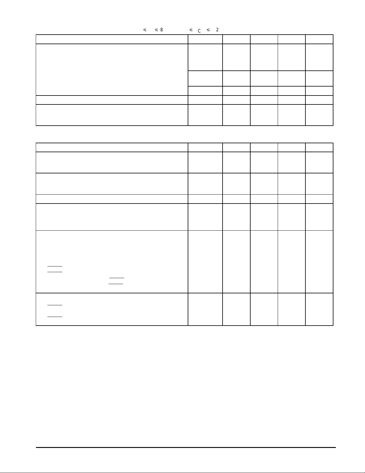
ELECTRICAL CHARACTERISTICS (–40°C
Characteristics
Inputs
Low Level Voltage (Pins 4 & 12, MC75174B only)
Low Level Voltage (All Other Pins)
High Level Voltage (All Inputs)
Current @ Vin = 2.7 V (All Inputs)
Current @ Vin = 0.5 V (All Inputs)
Clamp Voltage (All Inputs, Iin = –18 mA) V
Thermal Shutdown Junction Temperature T
Power Supply Current (Outputs Open, VCC = 5.25 V)
Outputs Enable
Outputs Disabled
TIMING CHARACTERISTICS (T
Characteristics
Propagation Delay – Input to Single–ended Output (Figure 3)
Output Low–to–High
Output High–to–Low
Propagation Delay – Input to Differential Output (Figure 4)
Input Low–to–High
Input High–to–Low
Differential Output Transition T ime (Figure 4) tdr, t
Skew Timing
t
– t
PLHD
Max – Min t
Max – Min t
Enable Timing
Single–ended Outputs (Figure 5)
Enable to Active High Output
Enable to Active Low Output
Active High to Disable (using Enable)
Active Low to Disable (using Enable)
Enable
to Active High Output (MC75172B only)
Enable
to Active Low Output (MC75172B only)
Active High to Disable (using Enable
Active Low to Disable (using Enable
Differential Outputs (Figure 6)
Enable to Active Output
Enable
to Active Output (MC75172B only)
Enable to 3–State Output
Enable
to 3–State Output (MC75172B only)
for Each Driver
PHLD
Within a Package
PLHD
Within a Package
PHLD
= 25°C, VCC = 5.0 V)
A
, MC75172B only)
, MC75172B only)
p
TAp
85°C, 4.75 V p VCC p 5.25 V, unless otherwise noted.)
Symbol Min Typ Max Unit
V
V
Symbol Min Typ Max Unit
t
PLH(D)
t
PHL(D)
t
PZH(E)
t
PZL(E)
t
PHZ(E)
t
PLZ(E)
t
PZH(E)
t
PZL(E)
t
PHZ(E)
t
PLZ(E)
t
PZD(E)
t
PZD(E)
t
PDZ(E)
t
PDZ(E)
IL(A)
IL(B)
V
I
IH
I
I
CC
t
PLH
t
PHL
t
SK1
t
SK2
t
SK3
0
0
IH
IL
IK
jts
df
2.0
–
–100
–1.5 – – Vdc
– +150 – °C
–
–
–
–
–
–
– 19 25 ns
–
–
–
–
–
–
–
–
–
–
–
–
–
–
–
–
–
–
0.2
–15
60
30
23
18
15
17
0.2
1.5
1.5
48
20
35
30
58
28
38
36
47
56
32
40
0.7
0.8
V
CC
20
–
70
40
30
30
25
25
–
–
–
60
30
45
50
70
35
50
50
–
–
–
–
Vdc
µA
mA
ns
ns
ns
ns
ns
MOTOROLA ANALOG IC DEVICE DATA
3
V
(0.8 or 2.0 V)
in
V
in
S.G.
MC75172B MC75174B
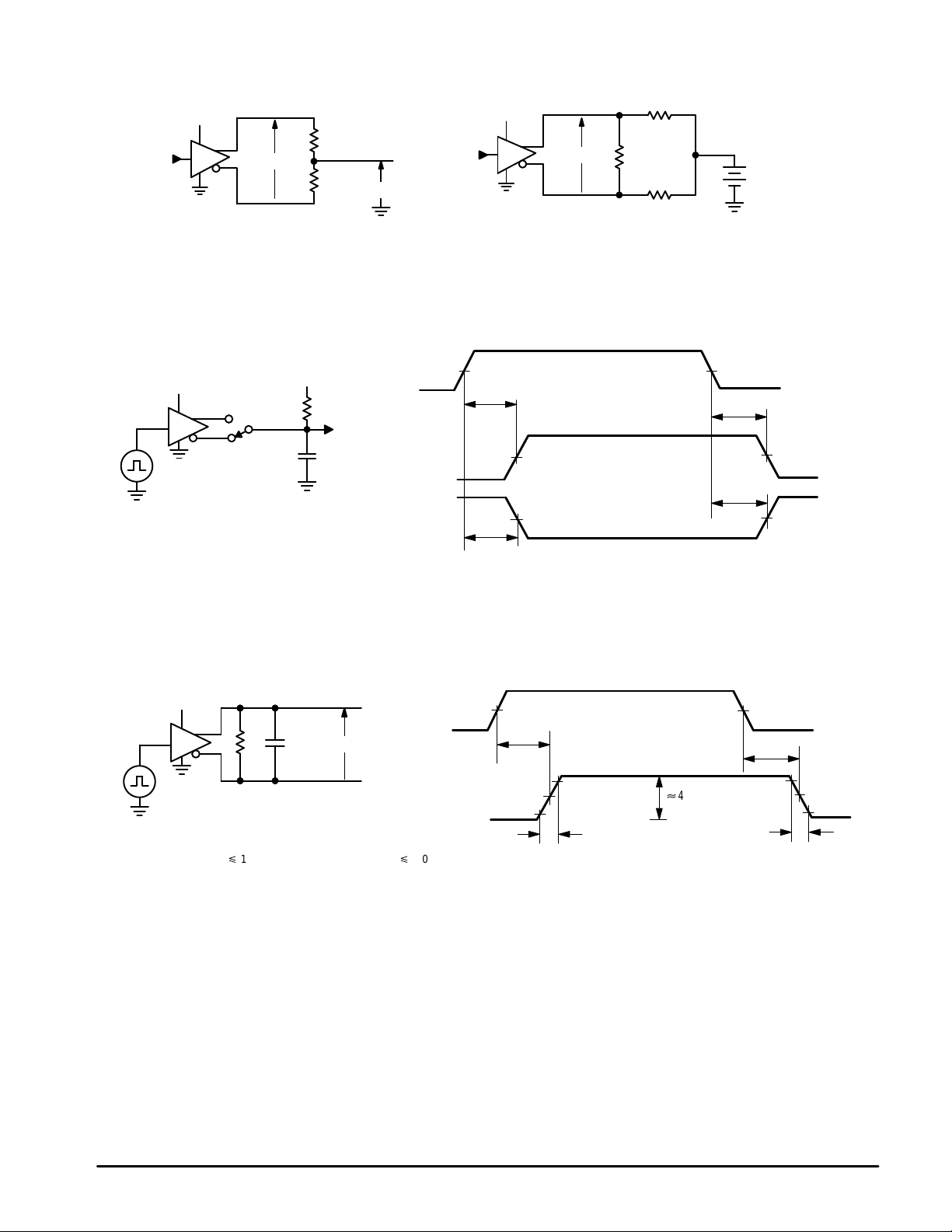
Figure 1. VDD Measurement Figure 2. Common Mode T est
V
V
in
1.5 V
t
PLH
t
PHL
CC
3.0 V
3.0 V
V
OD3
375
58
375
3.0 V
V
CC
RL/2
V
OD2,A
RL/2
V
OS
(0.8 or 2.0 V)
Figure 3. Propagation Delay , Single–Ended Outputs
V
V
CC
Y
2.3 V
27
Ω
Output
Z
15 pF
in
Output Y
Output Z
+
VCM = 12 to –7.0 V
1.5 V
t
PHL
3.0 V
t
PLH
3.0 V
0 V
V
OL
V
OH
Figure 4. Propagation Delay , Differential Outputs
V
CC
V
in
54
S.G.
NOTES: 1. S.G. set to: f p 1.0 MHz; duty cycle = 50%; tr, tf, p5.0 ns.
2.t
= t
SK1
3.t
computed by subtracting the shortest t
SK2
4.t
computed by subtracting the shortest t
SK3
PLHD
– t
PHLD
for each driver.
50 pF
V
OD
from the longest t
PLHD
from the longest t
PHLD
3.0 V
1.5 V
V
in
t
PLHD
1.5 V
V
OD
50%
[
4.6 V
–1.5 V
t
dr
of the 4 drivers within a package.
PLHD
of the 4 drivers within a package.
PHLD
1.5 V
t
PHLD
t
df
0 V
1.5 V
50%
–1.5 V
4
MOTOROLA ANALOG IC DEVICE DATA
 Loading...