

MOTOROLA MC74VHCU04 Technical data
查询MC74VHCU04供应商
SEMICONDUCTOR TECHNICAL DATA
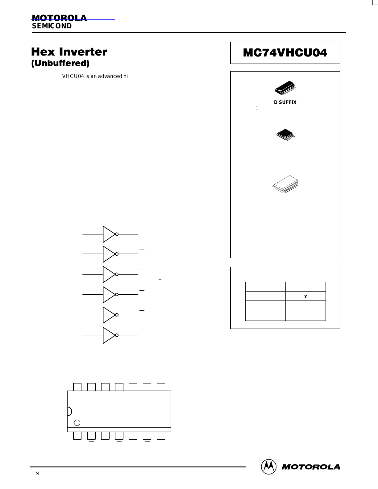
The MC74VHCU04 is an advanced high speed CMOS unbuffered inverter
fabricated with silicon gate CMOS technology. It achieves high speed
operation similar to equivalent Bipolar Schottky TTL while maintaining
CMOS low power dissipation.
The inputs tolerate voltages up to 7V , allowing the interface of 5V systems
to 3V systems.
• High Speed: tPD = 3.5ns (Typ) at VCC = 5V
• Low Power Dissipation: ICC = 2µA (Max) at TA = 25°C
• High Noise Immunity: V
• Power Down Protection Provided on Inputs
• Balanced Propagation Delays
• Designed for 2V to 5.5V Operating Range
• Low Noise: V
= 0.8V (Max)
OLP
• Pin and Function Compatible with Other Standard Logic Families
• Latchup Performance Exceeds 300mA
• ESD Performance: HBM > 2000V; Machine Model > 200V
• Chip Complexity: 12 FETs or 3 Equivalent Gates
1
3
A2
NIH
= V
= 10% VCC (Min.)
NIL
LOGIC DIAGRAM
2
4
Y1A1
Y2
D SUFFIX
14–LEAD SOIC PACKAGE
CASE 751A–03
14–LEAD TSSOP PACKAGE
14–LEAD SOIC EIAJ PACKAGE
MC74VHCUXXD
MC74VHCUXXDT
MC74VHCUXXM
DT SUFFIX
CASE 948G–01
M SUFFIX
CASE 965–01
ORDERING INFORMATION
SOIC
TSSOP
SOIC EIAJ
10
12
6
Y3
Y = A
8
Y4
Y5
Y6
A3
A4
A5
A6
5
9
11
13
Pinout: 14–Lead Packages (Top View)
VCCA6 Y6
1314 12 11 10 9 8
21 34567
A1 Y1 A2 Y2 A3 Y3 GND
A5 Y5 A4 Y4
FUNCTION TABLE
Inputs Outputs
A
L
H
Y
H
L
6/97
Motorola, Inc. 1997
1
REV 0
MC74VHCU04
Î
Î
Î
Î
ÎÎÎ
ÎÎÎ
V
CC
Î
Î
Î
Î
Î
Î
ÎÎÎ
Î
Î
Î
Î
Î
Î
Î
Î
Î
Î
Î
Î
Î
Î
Î
Î
Î
Î
ÎÎÎ
Î
Î
Î
Î
Î
Î
Î
Î
Î
Î
Î
Î
Î
Î
Î
ÎÎÎ
Î
Î
Î
Î
Î
Î
Î
Î
ÎÎÎ
Î
Î
Î
Î
Î
Î
Î
Î
Î
Î
Î
Î
ÎÎÎ
Î
Î
Î
Î
Î
Î
Î
Î
Î
Î
Î
Î
Î
ÎÎÎ
Î
Î
Î
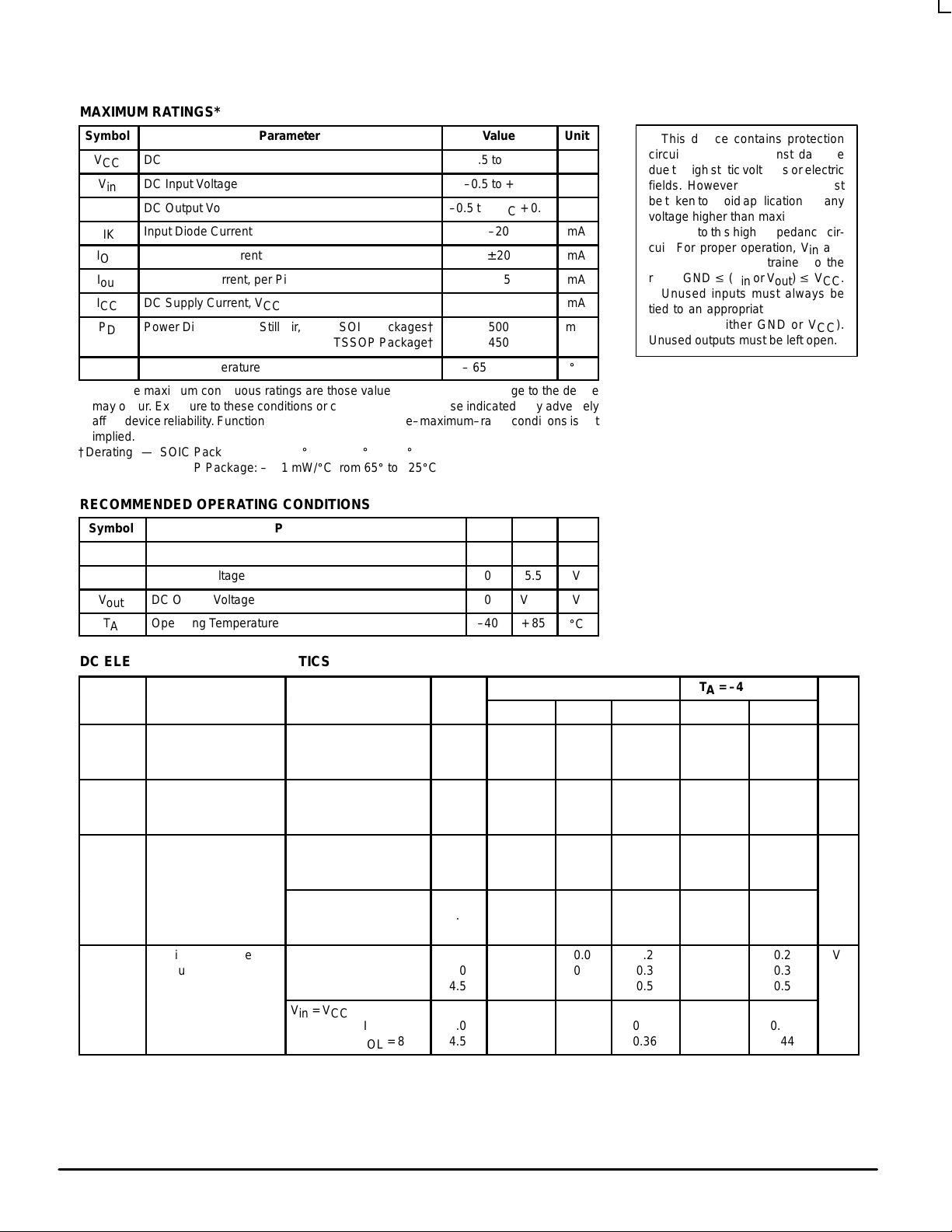
MAXIMUM RATINGS*
Symbol
V
V
I
I
I
Î
T
DC Supply Voltage
CC
V
DC Input Voltage
in
DC Output Voltage
out
I
Input Diode Current
IK
Output Diode Current
OK
DC Output Current, per Pin
out
DC Supply Current, VCC and GND Pins
CC
P
Power Dissipation in Still Air, SOIC Packages†
D
ОООООООООООО
Storage Temperature
stg
* Absolute maximum continuous ratings are those values beyond which damage to the device
may occur. Exposure to these conditions or conditions beyond those indicated may adversely
affect device reliability . Functional operation under absolute–maximum–rated conditions is not
implied.
†Derating — SOIC Packages: – 7 mW/_C from 65_ to 125_C
TSSOP Package: – 6.1 mW/_C from 65_ to 125_C
RECOMMENDED OPERATING CONDITIONS
Symbol
V
V
V
T
DC Supply Voltage
CC
DC Input Voltage
in
DC Output Voltage
out
Operating Temperature
A
Parameter
Parameter
TSSOP Package†
Value
–0.5 to + 7.0
–0.5 to + 7.0
–0.5 to VCC + 0.5
–20
± 20
± 25
± 50
500
450
ÎÎÎÎ
– 65 to + 150
Min
Max
2.0
5.5
0
5.5
0
V
CC
–40
+ 85
Unit
V
V
V
mA
mA
mA
mA
mW
Î
_
C
Unit
V
V
V
_
C
This device contains protection
circuitry to guard against damage
due to high static voltages or electric
fields. However, precautions must
be taken to avoid applications of any
voltage higher than maximum rated
voltages to this high–impedance circuit. For proper operation, Vin and
V
should be constrained to the
out
range GND v (Vin or V
Unused inputs must always be
) v VCC.
out
tied to an appropriate logic voltage
level (e.g., either GND or VCC).
Unused outputs must be left open.
DC ELECTRICAL CHARACTERISTICS
Symbol
V
IH
ÎÎ
ÎÎ
V
IL
ÎÎ
ÎÎ
V
OH
ÎÎ
ÎÎ
ÎÎ
V
OL
ÎÎ
ÎÎ
ÎÎÎÎÎÎÎÎОООООО
Parameter
Minimum High–Level
ÎÎÎÎ
Input Voltage
ÎÎÎÎ
Maximum Low–Level
ÎÎÎÎ
Input Voltage
ÎÎÎÎ
Minimum High–Level
Output Voltage
ÎÎÎÎ
ÎÎÎÎ
ÎÎÎÎ
Maximum Low–Level
ÎÎÎÎ
Output Voltage
ÎÎÎÎ
Test Conditions
ОООООО
ОООООО
ОООООО
ОООООО
Vin =V
IL
IOH = –50µA
ОООООО
Vin = GND
ОООООО
ОООООО
Vin = V
ОООООО
IOL = 50µA
ОООООО
Vin = V
IOH = –4mA
IOH = –8mA
IH
CC
IOL = 4mA
IOL = 8mA
V
V
2.0
ÎÎ
3.0 to
5.5
ÎÎ
2.0
ÎÎ
3.0 to
5.5
ÎÎ
2.0
3.0
ÎÎ
4.5
3.0
ÎÎ
4.5
ÎÎ
2.0
ÎÎ
3.0
4.5
ÎÎ
3.0
ÎÎ
4.5
TA = 25°C
Min
Typ
Max
1.70
ÎÎ
VCC x 0.8
ÎÎ
ÎÎ
ÎÎ
1.8
2.7
ÎÎ
4.0
2.58
ÎÎ
3.94
ÎÎ
ÎÎ
ÎÎ
ÎÎÎÎÎÎÎ
Î
Î
Î
Î
2.0
3.0
Î
4.5
Î
Î
0.0
Î
0.0
0.0
Î
ÎÎ
ÎÎ
0.30
ÎÎ
VCC x 0.2
ÎÎ
ÎÎÎÎÎ
ÎÎ
ÎÎ
0.2
ÎÎ
0.3
0.5
ÎÎ
0.36
0.36
TA = –40 to 85°C
Min
Max
1.70
ÎÎ
VCC x 0.8
ÎÎ
ÎÎ
ÎÎ
ÎÎ
ÎÎ
0.30
ÎÎ
VCC x 0.2
ÎÎ
1.8
2.7
4.0
2.48
ÎÎ
3.80
ÎÎ
ÎÎ
ÎÎ
ÎÎÎÎÎ
ÎÎ
ÎÎ
ÎÎ
0.2
ÎÎ
0.3
0.5
ÎÎ
0.44
0.44
Unit
V
V
V
V
MOTOROLA VHC Data – Advanced CMOS Logic
2
DL203 — Rev 0
 Loading...