

MOTOROLA MC74VHC244ML2, MC74VHC244DW, MC74VHC244DWR2, MC74VHC244M, MC74VHC244MEL Datasheet
...
SEMICONDUCTOR TECHNICAL DATA
1
REV 1
Motorola, Inc. 1997
6/97
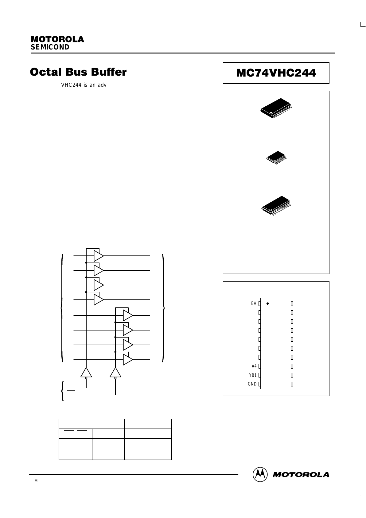
The MC74VHC244 is an advanced high speed CMOS octal bus buffer
fabricated with silicon gate CMOS technology. It achieves high speed
operation similar to equivalent Bipolar Schottky TTL while maintaining
CMOS low power dissipation.
The MC74VHC244 is a noninverting 3–state buffer, and has two
active–low output enables. This device is designed to be used with 3–state
memory address drivers, etc.
The internal circuit is composed of three stages, including a buffer output
which provides high noise immunity and stable output. The inputs tolerate
voltages up to 7V, allowing the interface of 5V systems to 3V systems.
• High Speed: tPD = 3.9ns (Typ) at VCC = 5V
• Low Power Dissipation: ICC = 4µA (Max) at TA = 25°C
• High Noise Immunity: V
NIH
= V
NIL
= 28% V
CC
• Power Down Protection Provided on Inputs
• Balanced Propagation Delays
• Designed for 2V to 5.5V Operating Range
• Low Noise: V
OLP
= 0.9V (Max)
• Pin and Function Compatible with Other Standard Logic Families
• Latchup Performance Exceeds 300mA
• ESD Performance: HBM > 2000V; Machine Model > 200V
• Chip Complexity: 136 FETs or 34 Equivalent Gates
LOGIC DIAGRAM
DATA
INPUTS
A1
A2
A3
A4
B1
B2
B3
B4
17
15
13
11
8
6
4
218
16
14
12
9
7
5
3
YB4
YB3
YB2
YB1
YA4
YA3
YA2
YA1
NONINVERTING
OUTPUTS
OUTPUT
ENABLES
OEA
OEB
1
19
OEA, OEB A, B YA, YB
L
L
H
L
H
X
L
H
Z
INPUTS OUTPUTS
FUNCTION TABLE
PIN ASSIGNMENT
A3
A2
YB4
A1
OEA
GND
YB1
A4
YB2
YB3 5
4
3
2
1
10
9
8
7
6
14
15
16
17
18
19
20
11
12
13
YA2
B4
YA1
OEB
V
CC
B1
YA4
B2
YA3
B3
DW SUFFIX
20–LEAD SOIC PACKAGE
CASE 751D–04
ORDERING INFORMATION
MC74VHCXXXDW
MC74VHCXXXDT
MC74VHCXXXM
SOIC
TSSOP
SOIC EIAJ
DT SUFFIX
20–LEAD TSSOP PACKAGE
CASE 948E–02
M SUFFIX
20–LEAD SOIC EIAJ PACKAGE
CASE 967–01
MC74VHC244
MOTOROLA VHC Data – Advanced CMOS Logic
DL203 — Rev 1
2
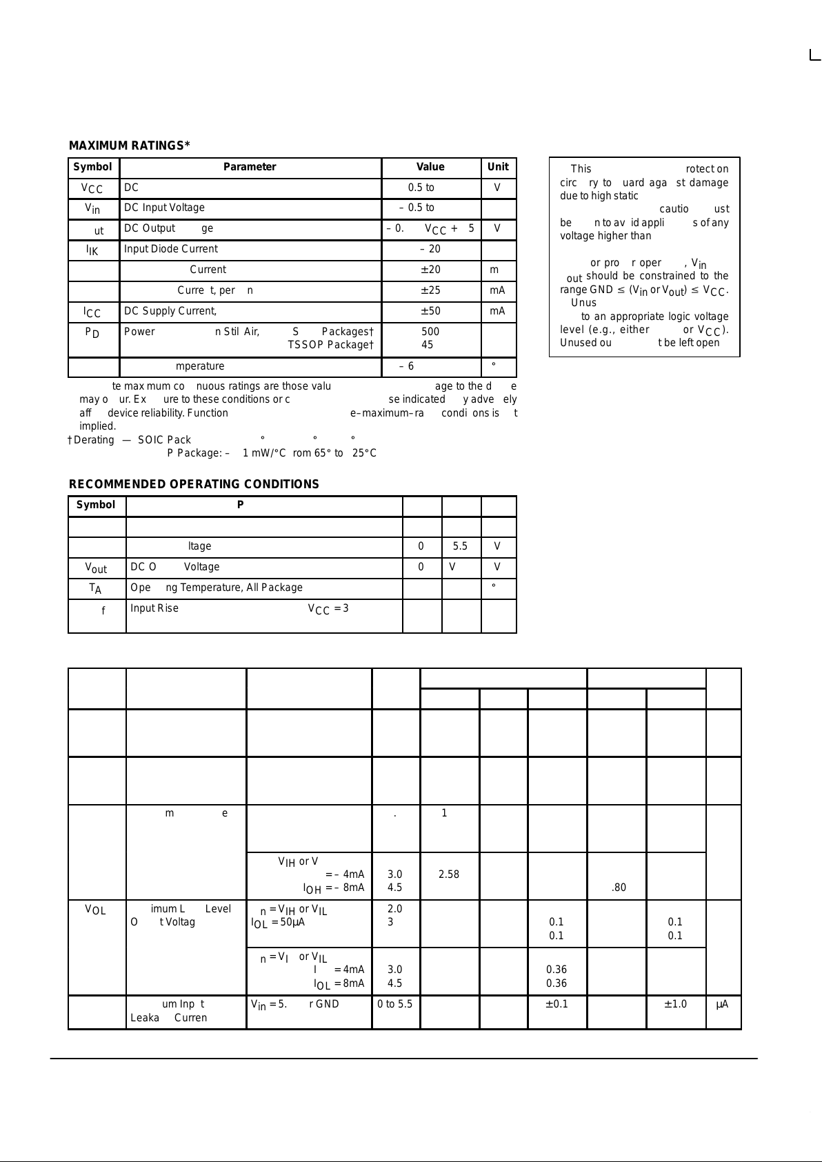
MAXIMUM RATINGS*
Symbol
Parameter
Value
Unit
V
CC
DC Supply Voltage
– 0.5 to + 7.0
V
V
in
DC Input Voltage
– 0.5 to + 7.0
V
V
out
DC Output Voltage
– 0.5 to VCC + 0.5
V
I
IK
Input Diode Current
– 20
mA
I
OK
Output Diode Current
± 20
mA
I
out
DC Output Current, per Pin
± 25
mA
I
CC
DC Supply Current, VCC and GND Pins
± 50
mA
Î
Î
P
D
ОООООООООООО
Î
Power Dissipation in Still Air, SOIC Packages†
TSSOP Package†
ÎÎÎÎ
Î
500
450
Î
Î
mW
T
stg
Storage Temperature
– 65 to + 150
_
C
* Absolute maximum continuous ratings are those values beyond which damage to the device
may occur. Exposure to these conditions or conditions beyond those indicated may adversely
affect device reliability . Functional operation under absolute–maximum–rated conditions is not
implied.
†Derating — SOIC Packages: – 7 mW/_C from 65_ to 125_C
TSSOP Package: – 6.1 mW/_C from 65_ to 125_C
RECOMMENDED OPERATING CONDITIONS
Symbol
Parameter
Min
Max
Unit
V
CC
DC Supply Voltage
2.0
5.5
V
V
in
DC Input Voltage
0
5.5
V
V
out
DC Output Voltage
0
V
CC
V
T
A
Operating Temperature, All Package Types
– 40
+ 85
_
C
tr, t
f
Input Rise and Fall Time VCC = 3.3V ±0.3V
VCC =5.0V ±0.5V00
10020ns/V
DC ELECTRICAL CHARACTERISTICS
ÎÎÎ
V
TA = 25°C
TA = – 40 to 85°C
Symbol
Parameter
Test Conditions
ÎÎÎ
V
CC
V
Min
Typ
Max
Min
Max
Unit
ÎÎ
Î
V
IH
ÎÎÎÎ
Î
Minimum High–Level
Input Voltage
ОООООО
Î
ÎÎÎ
ÎÎ
Î
2.0
3.0 to
5.5
ÎÎ
Î
1.50
VCC x 0.7
ÎÎÎÎÎÎÎ
Î
1.50
VCC x 0.7
ÎÎ
Î
V
ÎÎ
Î
ÎÎ
Î
V
IL
ÎÎÎÎ
Î
ÎÎÎÎ
Î
Maximum Low–Level
Input Voltage
ОООООО
Î
ОООООО
Î
ÎÎÎ
ÎÎ
Î
ÎÎ
Î
2.0
3.0 to
5.5
ÎÎ
Î
ÎÎ
Î
Î
Î
Î
Î
ÎÎ
Î
ÎÎ
Î
0.50
VCC x 0.3
ÎÎ
Î
ÎÎ
Î
ÎÎ
Î
ÎÎ
Î
0.50
VCC x 0.3
V
ÎÎ
Î
ÎÎ
Î
V
OH
ÎÎÎÎ
Î
ÎÎÎÎ
Î
Minimum High–Level
Output Voltage
ОООООО
Î
ОООООО
Î
Vin = VIH or V
IL
IOH = – 50µA
ÎÎÎ
ÎÎ
Î
ÎÎ
Î
2.0
3.0
4.5
ÎÎ
Î
ÎÎ
Î
1.9
2.9
4.4
Î
Î
Î
Î
2.0
3.0
4.5
ÎÎ
Î
ÎÎ
Î
ÎÎ
Î
ÎÎ
Î
1.9
2.9
4.4
ÎÎ
Î
ÎÎ
Î
V
ÎÎÎÎÎÎÎÎОООООО
Î
Vin = VIH or V
IL
IOH = – 4mA
IOH = – 8mA
ÎÎÎ
ÎÎ
Î
3.0
4.5
ÎÎ
Î
2.58
3.94
ÎÎÎÎÎÎÎ
Î
2.48
3.80
ÎÎ
Î
ÎÎ
Î
ÎÎ
V
OL
ÎÎÎÎ
Î
ÎÎÎÎ
Maximum Low–Level
Output Voltage
ОООООО
Î
ОООООО
Vin = VIH or V
IL
IOL = 50µA
ÎÎÎ
ÎÎ
Î
ÎÎ
2.0
3.0
4.5
ÎÎ
Î
ÎÎ
Î
Î
Î
0.0
0.0
0.0
ÎÎ
Î
ÎÎ
0.1
0.1
0.1
ÎÎ
Î
ÎÎ
ÎÎ
Î
ÎÎ
0.1
0.1
0.1
V
ÎÎ
Î
ÎÎ
Î
ÎÎÎÎ
Î
ÎÎÎÎ
Î
ОООООО
Î
ОООООО
Î
Vin = VIH or V
IL
IOL = 4mA
IOL = 8mA
ÎÎÎ
ÎÎ
Î
ÎÎ
Î
3.0
4.5
ÎÎ
Î
ÎÎ
Î
Î
Î
Î
Î
ÎÎ
Î
ÎÎ
Î
0.36
0.36
ÎÎ
Î
ÎÎ
Î
ÎÎ
Î
ÎÎ
Î
0.44
0.44
ÎÎ
I
in
ÎÎÎÎ
Maximum Input
Leakage Current
ОООООО
Vin = 5.5V or GND
ÎÎÎ
ÎÎ
0 to 5.5
ÎÎ
Î
ÎÎ
± 0.1
ÎÎ
ÎÎ
± 1.0
µA
This device contains protection
circuitry to guard against damage
due to high static voltages or electric
fields. However, precautions must
be taken to avoid applications of any
voltage higher than maximum rated
voltages to this high–impedance circuit. For proper operation, Vin and
V
out
should be constrained to the
range GND v (Vin or V
out
) v VCC.
Unused inputs must always be
tied to an appropriate logic voltage
level (e.g., either GND or VCC).
Unused outputs must be left open.
 Loading...