

MOTOROLA MC74VHC1G66DFT1 Datasheet
MC74VHC1G66
Advance Information
Analog Switch
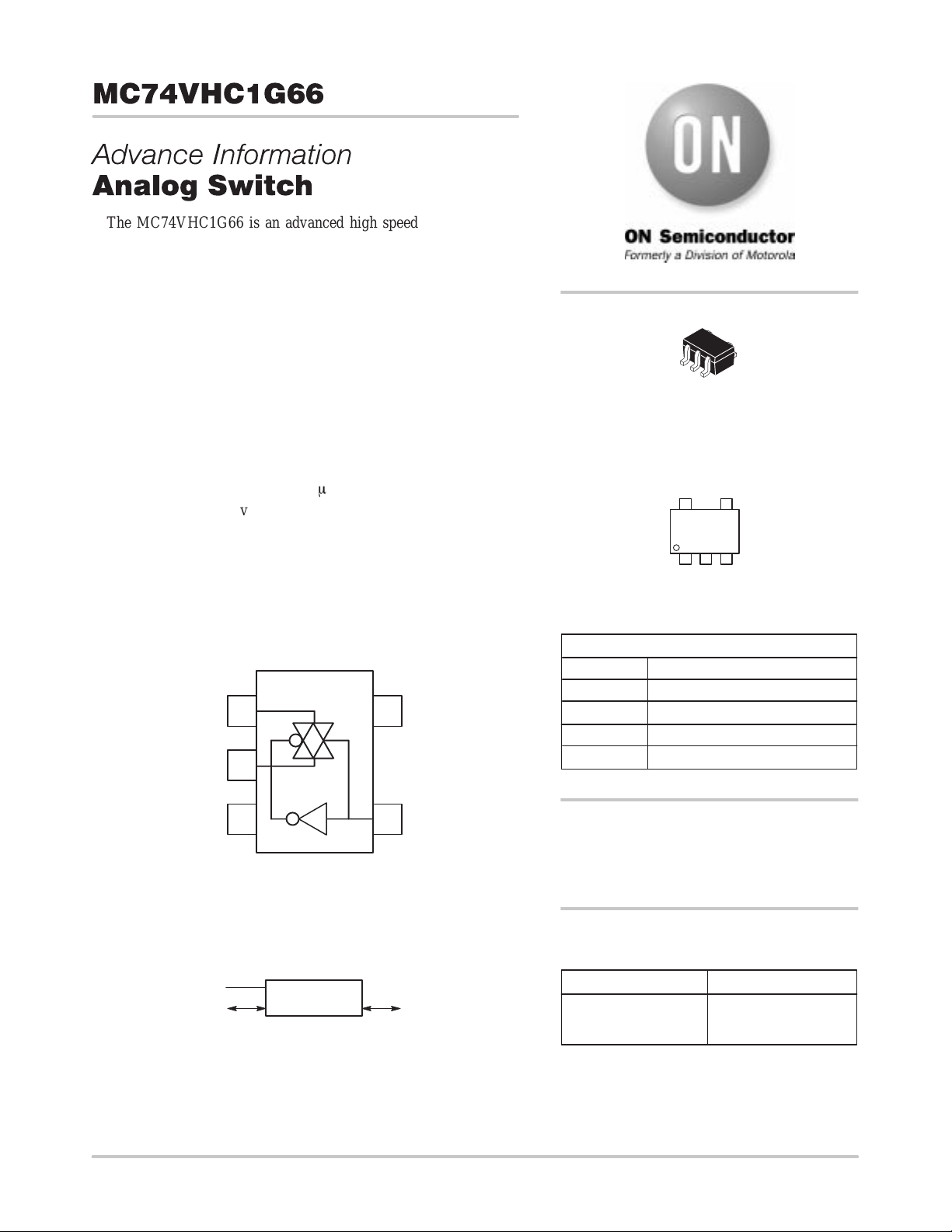
The MC74VHC1G66 is an advanced high speed CMOS bilateral
analog switch fabricated with silicon gate CMOS technology. It
achieves high speed propagation delays and low ON resistances while
maintaining CMOS low power dissipation. This bilateral switch
controls analog and digital voltages that may vary across the full
power–supply range (from VCC to GND).
The MC74VHC1G66 is compatible in function to a single gate of
the High Speed CMOS MC74VHC4066 and the metal–gate CMOS
MC14066. The device has been designed so that the ON resistances
(RON) are much lower and more linear over input voltage than RON of
the metal–gate CMOS or High Speed CMOS analog switches.
The ON/OFF control inputs are compatible with standard CMOS
outputs; with pull–up resistors, it is compatible with LSTTL outputs.
• High Speed: t
• Low Power Dissipation: I
• Diode Protection Provided on Inputs and Outputs
• Improved Linearity and Lower ON Resistance over Input Voltage
than the MC14066 or the HC4066
• Pin and Function Compatible with Other Standard Logic Families
• Latchup Performance Exceeds 300 mA
• ESD Performance: HBM > 2000 V; MM > 200 V, CDM > 1500 V
• Chip Complexity: 11 FETs or 3 Equivalent Gates
= TBD (Typ) at VCC = 5 V
PD
= 2 mA (Max) at TA = 25°C
CC
IN/OUT X
A
OUT/IN Y
2
A
V
51
CC
http://onsemi.com
SC–88A / SOT–353
DF SUFFIX
CASE 419A
MARKING DIAGRAM
d
V9
Pin 1
d = Date Code
PIN ASSIGNMENT
1
2
3 GND
4
5 VCC
IN/OUT X
OUT/IN Y
ON/OFF CONTROL
A
A
ON/OFF CONTROLGND
43
5–Lead SOT–353 Pinout (Top View)
LOGIC SYMBOL
ON/OFF CONTROL
IN/OUT X
A
This document contains information on a new product. Specifications and information
herein are subject to change without notice.
Semiconductor Components Industries, LLC, 1999
November, 1999 – Rev. 1
X 1
1
U U
1
OUT/IN Y
A
1 Publication Order Number:
ORDERING INFORMATION
See detailed ordering and shipping information in the package
dimensions section on page 7 of this data sheet.
FUNCTION TABLE
On/Off Control Input State of Analog Switch
L
H
Off
On
MC74VHC1G66/D
MC74VHC1G66
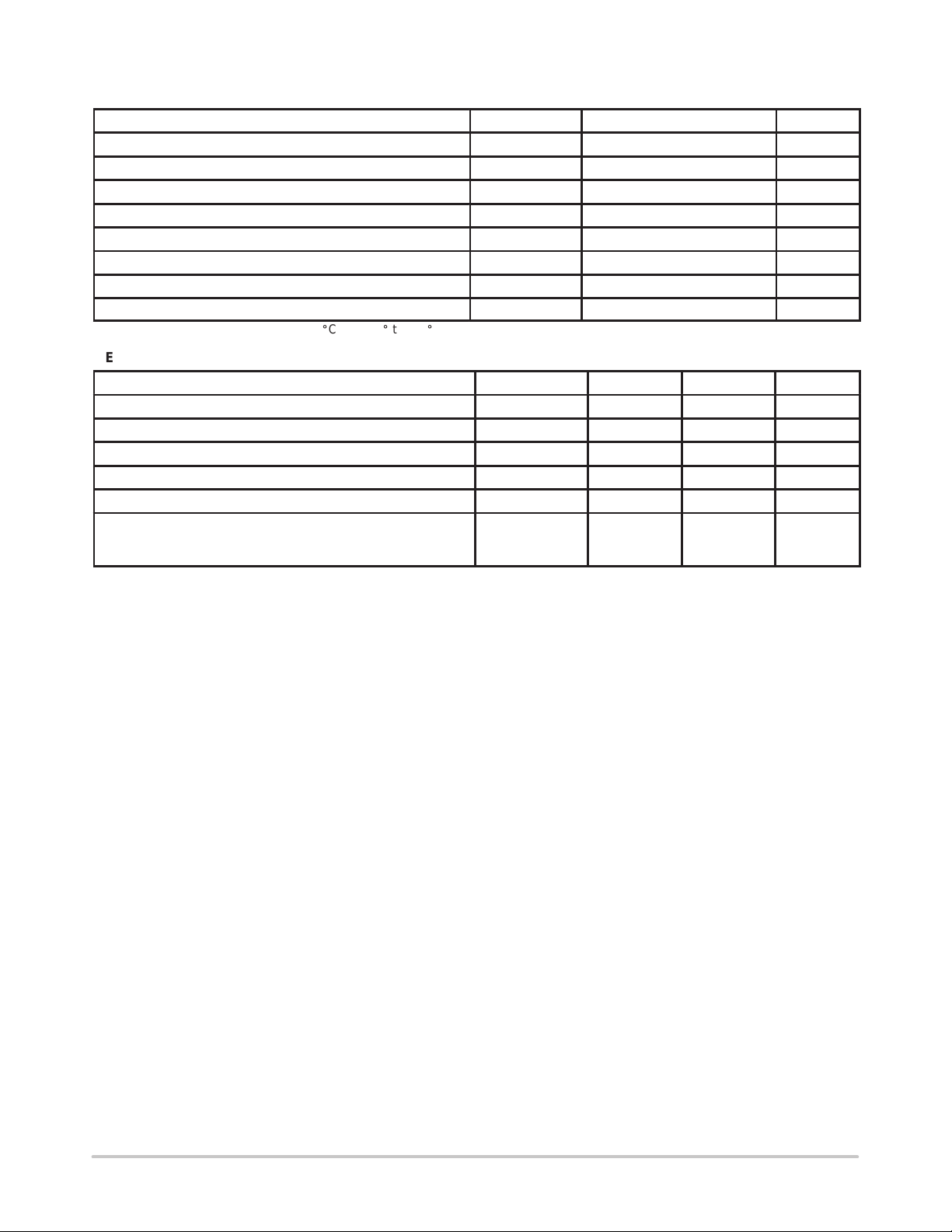
ABSOLUTE MAXIMUM RATINGS
Characteristics Symbol Value Unit
DC Supply Voltage V
Digital Input Voltage V
Analog Output Voltage V
Digital Input Diode Current I
DC Supply Current, VCC and GND I
Power dissipation in still air, SC–88A † P
Lead temperature, 1 mm from case for 10 s T
Storage temperature T
†Derating — SC–88A Package: –3 mW/_C from 65_ to 125_C
CC
IN
IS
IK
CC
D
L
stg
RECOMMENDED OPERATING CONDITIONS
Characteristics Symbol Min Max Unit
DC Supply Voltage V
Digital Input Voltage V
Analog Input Voltage V
Static or Dynamic Voltage Across Switch VIO* 1.2 V
Operating Temperature Range T
Input Rise and Fall Time
ON/OFF Control Input VCC = 3.3V ± 0.3V
VCC = 5.0V ± 0.5V
* For voltage drops across the switch greater than 1.2V (switch on), excessive VCC current may be drawn; i.e. the current out of the switch may
contain both VCC and switch input components. The reliability of the device will be unaffected unless the Maximum Ratings are exceeded.
CC
IN
IS
tr , t
A
f
–0.5 to +7.0 V
–0.5 to VCC +0.5 V
–0.5 to VCC + 0.5 V
–20 mA
+25 mA
200 mW
260 °C
–65 to +150 °C
4.5 5.5 V
GND V
GND V
–55 +85 °C
0
0
CC
CC
100
20
V
V
ns/V
http://onsemi.com
2
MC74VHC1G66
V
CC
Î
Î
Î
Î
Î
Î
Î
Î
Î
Î
Î
Î
Î
Î
Î
Î
Î
Î
Î
Î
Î
Î
Î
Î
Î
Î
Î
Î
Î
Î
Î
Î
Î
Î
Î
Î
Î
Î
Î
Î
Î
Î
Î
Î
Î
Î
Î
Î
Î
Î
Î
Î
Î
Î
Î
Î
C
Î
Î
Î
Î
Î
Î
Î
Î
Î
Î
Î
Î
Î
Î
Î
Î
Î
Î
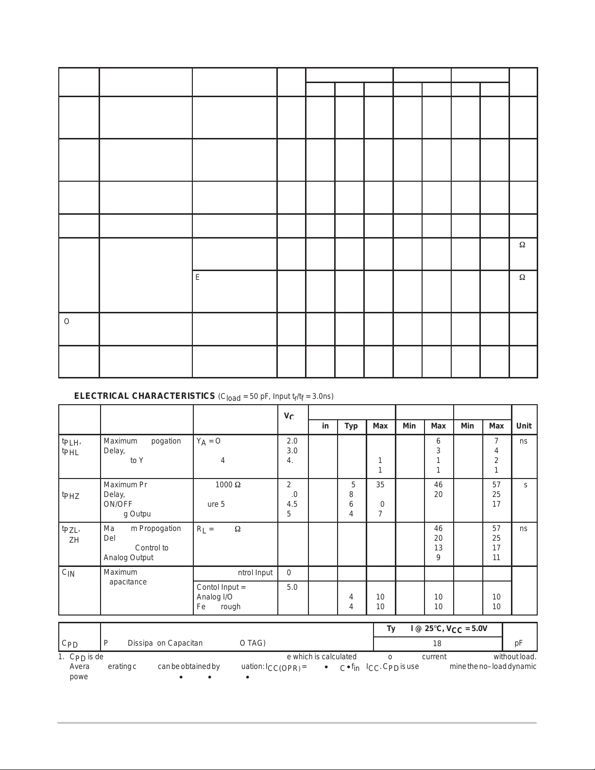
DC ELECTRICAL CHARACTERISTICS
V
CC
Symbol Parameter Test Conditions (V) Min Typ Max Min Max Min Max Unit
V
IH
Minimum High–Level
Input Voltage
ON/OFF Control Input
RON = Per Spec 2.0
3.0
4.5
5.5
V
IL
Maximum Low–Level
Input Voltage
ON/OFF Control Input
RON = Per Spec 2.0
3.0
4.5
5.5
I
IN
Maximum Input
Leakage Current
VIN = VCC or GND 0 to
5.5
ON/OFF Control Input
I
R
CC
ON
Maximum Quiescent
Supply Current
Maximum ”ON”
Resistance
VIN = VCC or GND
VIO = 0V
VIN = V
IH
VIS = VCC or GND
|IIS| ≤ 10mA (Figure 1)
Endpoints
VIN = V
IH
VIS = VCC or GND
5.5 2.0 20 40 µA
3.0
4.5
5.5
3.0
4.5
5.5
|IIS| ≤ 10mA (Figure 1)
I
OFF
Maximum Off–Channel
Leakage Current
VIN = V
IL
VIS = VCC or GND
5.5 0.1 0.5 1.0 µA
Switch Off (Figure 2)
I
ON
Maximum On–Channel
Leakage
Current
VIN = V
IH
VIS = VCC or GND
Switch On (Figure 3)
5.5 0.1 0.5 1.0 µA
TA = 25°C TA ≤ 85°C TA ≤ 125°C
1.5
2.1
3.15
3.85
1.35
1.65
0.5
0.9
1.5
2.1
3.15
3.85
0.5
0.9
1.35
1.65
±0.1 ±1.0 ±1.0 µA
30
20
15
25
12
50
30
20
50
20
8
15
70
40
35
65
26
23
1.5
2.1
3.15
3.85
0.5
0.9
1.35
1.65
100
50
45
90
40
32
V
V
W
W
AC ELECTRICAL CHARACTERISTICS (C
Symbol
t
,
PLH
t
PHL
ÎÎ
ÎÎ
t
,
PLZ
t
PHZ
ÎÎ
t
,
PZL
ÎÎ
t
PZH
ÎÎ
C
IN
ÎÎ
ÎÎ
Parameter
Maximum Propogation
Delay,
ООООО
Input X to Y
ООООО
Maximum Propogation
Delay,
ON/OFF Control to
ООООО
Analog Output
Maximum Propogation
ООООО
Delay,
ON/OFF Control to
ООООО
Analog Output
Maximum Input
apacitance
ООООО
ООООО
Test Conditions
YA = Open
ООООО
Figure 4
ООООО
RL = 1000
Figure 5
ООООО
RL = 1000
ООООО
Figure 5
ООООО
ON/OFF Control Input
Contol Input = GND
ООООО
Analog I/O
Feedthrough
ООООО
= 50 pF, Input tr/tf = 3.0ns)
load
V
(V)
2.0
3.0
Î
4.5
5.5
Î
W
2.0
3.0
4.5
Î
5.5
W
2.0
Î
3.0
4.5
Î
5.5
0.0
5.0
Î
Î
TA = 25°C
Min
Typ
1
0
Î
Î
Î
0
0
Î
15
8
ÎÎÎ
6
4
Î
Î
15
Î
8
6
Î
4
3
Î
Î
Î
4
4
Î
Max
5
2
Î
1
1
Î
35
15
10
Î
7
35
Î
15
10
Î
7
10
Î
10
10
Î
TA ≤ 85°C
Min
Max
6
3
Î
Î
Î
1
1
Î
46
20
ÎÎÎ
13
9
Î
Î
46
Î
20
13
Î
9
10
Î
Î
Î
10
10
Î
TA ≤ 125°C
Min
Max
7
4
Î
Î
Î
2
1
Î
57
25
ÎÎÎ
17
11
Î
Î
57
Î
25
17
Î
11
10
Î
Î
Î
10
10
Î
Unit
ns
ns
ns
pF
Typical @ 25°C, VCC = 5.0V
C
PD
Power Dissipation Capacitance (Note NO T AG)
18
pF
1. CPD is defined as the value of the internal equivalent capacitance which is calculated from the operating current consumption without load.
Average operating current can be obtained by the equation: I
2
power consumption; PD = CPD V
fin + ICC VCC.
CC
CC(OPR
= CPD VCC fin + ICC. CPD is used to determine the no–load dynamic
)
http://onsemi.com
3
MC74VHC1G66
Î
Î
Î
Î
Î
Î
Î
Î
Î
Î
Î
Î
Î
Î
Î
Î
Î
Î
Î
Î
Î
Î
Î
Î
Î
Î
Î
Î
Î
Î
Î
Î
Î
Î
Î
Î
Î
Î
Î
Î
Î
Î
Î
Î
Î
Î
Î
Î
Î
Î
Î
Î
Î
Î
Î
Î
Î
Î
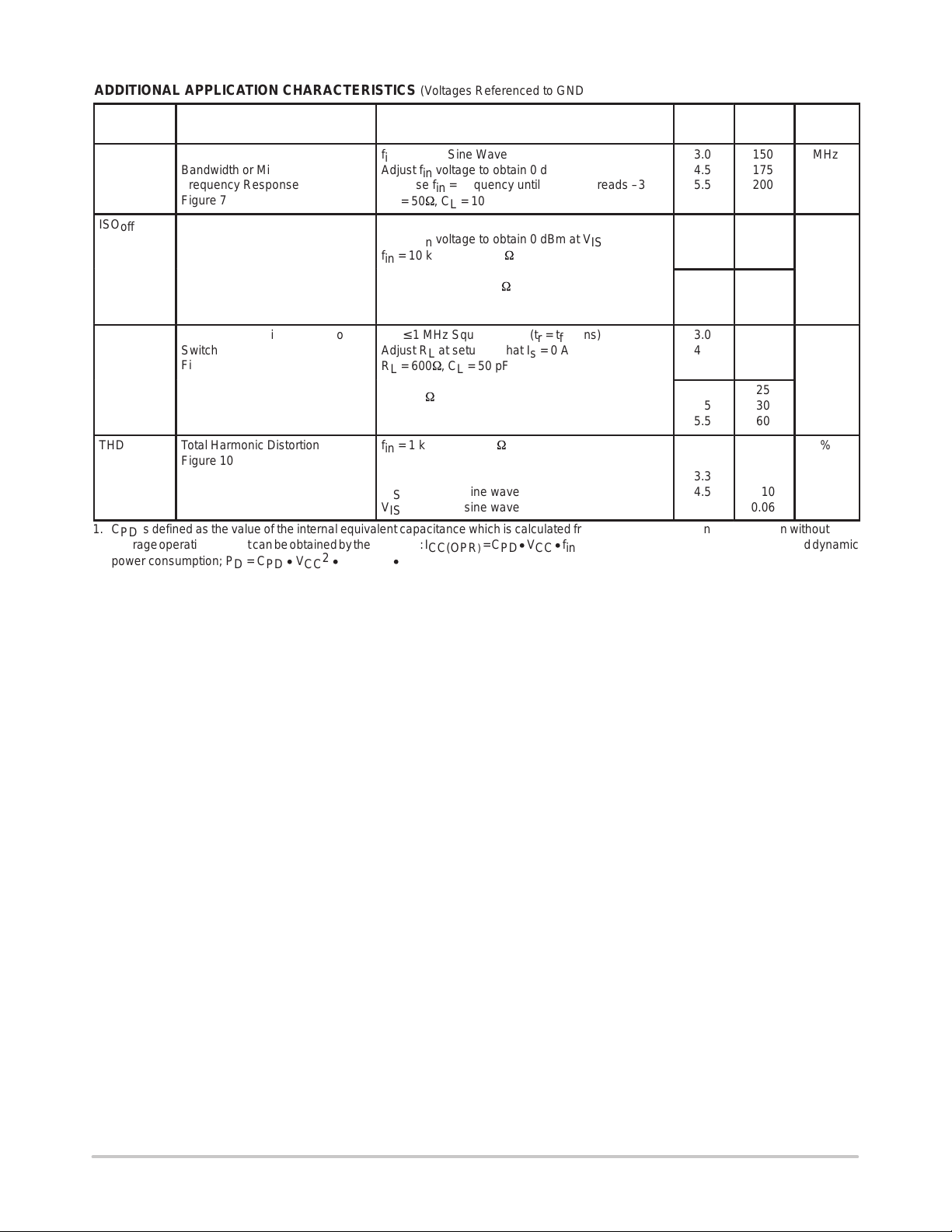
ADDITIONAL APPLICATION CHARACTERISTICS (Voltages Referenced to GND Unless Noted)
Limit
Symbol
ÎÎÎ
BW
ООООООО
Maximum On–Channel
Bandwidth or Minimum
ÎÎÎ
Frequency Response
ООООООО
Figure 7
ISO
off
ÎÎÎ
ÎÎÎ
ÎÎÎÎОООООООÎОООООООООООО
NOISE
ÎÎÎ
ÎÎÎ
ÎÎÎ
THD
ÎÎÎ
ÎÎÎ
Off–Channel Feedthrough
ООООООО
Isolation
Figure 8
ООООООО
Feedthrough Noise Control to
feed
Switch
ООООООО
Figure 9
ООООООО
ООООООО
Total Harmonic Distortion
Figure 10
ООООООО
ООООООО
Parameter
ОООООООООООО
Test Conditions
fin = 1 MHz Sine Wave
Adjust fin voltage to obtain 0 dBm at V
Increase fin = frequency until dB meter reads –3dB
ОООООООООООО
OS
RL = 50W, CL = 10 pF
fin = Sine Wave
ОООООООООООО
Adjust fin voltage to obtain 0 dBm at V
fin = 10 kHz, RL = 600W, CL = 50 pF
ОООООООООООО
IS
fin = 1.0 kHz, RL = 50W, CL = 10 pF
Vin ≤ 1 MHz Square Wave (tr = tf = 2ns)
Adjust RL at setup so that Is = 0 A
ОООООООООООО
RL = 600W, CL = 50 pF
RL = 50W, CL = 10 pF
ОООООООООООО
ОООООООООООО
fin = 1 kHz, RL = 10kW, CL = 50 pF
THD = THD
ОООООООООООО
VIS = 3.0 VPP sine wave
VIS = 4.0 VPP sine wave
ОООООООООООО
VIS = 5.0 VPP sine wave
Measured
– THD
Source
V
Î
3.0
4.5
5.5
Î
3.0
Î
4.5
5.5
Î
3.0
4.5
Î
5.5
3.0
4.5
Î
5.5
3.0
Î
4.5
5.5
Î
Î
3.3
4.5
Î
5.5
CC
1. CPD is defined as the value of the internal equivalent capacitance which is calculated from the operating current consumption without load.
Average operating current can be obtained by the equation: I
2
power consumption; PD = CPD V
fin + ICC VCC.
CC
CC(OPR
= CPD VCC fin + ICC. CPD is used to determine the no–load dynamic
)
25°C
ÎÎ
150
175
200
ÎÎ
–50
ÎÎ
–50
–50
ÎÎ
–40
–40
ÎÎ
–40
45
60
ÎÎ
130
25
ÎÎ
30
60
ÎÎ
ÎÎ
0.20
0.10
ÎÎ
0.06
Unit
Î
MHz
Î
Î
Î
Î
mV
Î
Î
Î
Î
Î
dB
PP
%
http://onsemi.com
4
 Loading...