

MOTOROLA MC74VHC1G14DFT1 Datasheet
MC74VHC1G14
Schmitt-Trigger Inverter
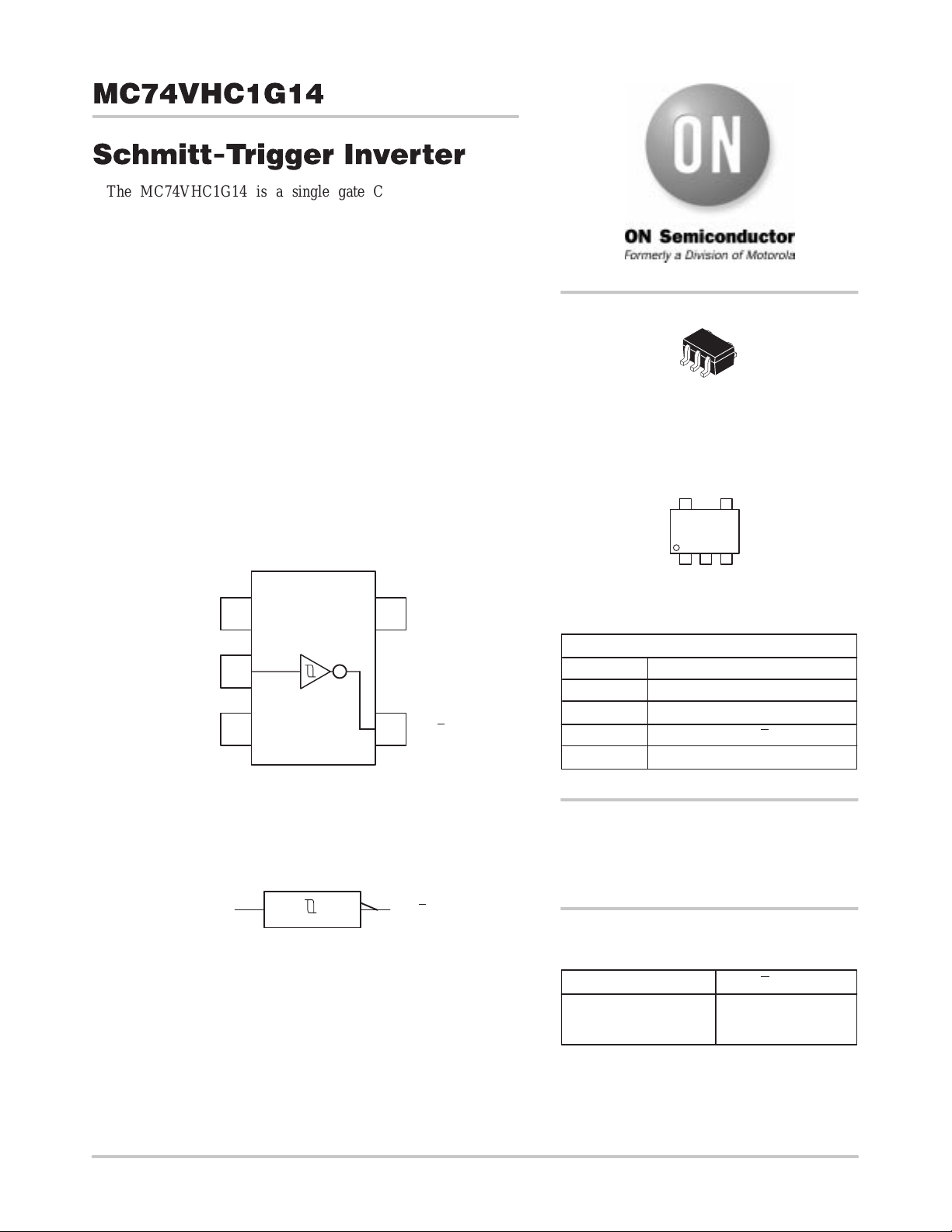
The MC74VHC1G14 is a single gate CMOS Schmitt–trigger
inverter fabricated with silicon gate CMOS technology. It achieves
high speed operation similar to equivalent Bipolar Schottky TTL
while maintaining CMOS low power dissipation.
The internal circuit is composed of three stages, including a buffer
output which provides high noise immunity and stable output.
The MC74VHC1G14 input structure provides protection when
voltages up to 7V are applied, regardless of the supply voltage. This
allows the MC74VHC1G14 to be used to interface 5V circuits to 3V
circuits.
The MC74VHC1G14 can be used to enhance noise immunity or to
square up slowly changing waveforms.
• High Speed: t
• Low Power Dissipation: I
• Power Down Protection Provided on Inputs
• Balanced Propagation Delays
• Pin and Function Compatible with Other Standard Logic Families
• Latchup Performance Exceeds 300mA
= 4.0ns (T yp) at VCC = 5V
PD
= 2µA (Max) at TA = 25°C
CC
http://onsemi.com
SC–88A / SOT–353
DF SUFFIX
CASE 419A
MARKING DIAGRAM
d
VA
NC
IN A
2
GND
Figure 1. 5–Lead SOT–353 Pinout (Top View)
LOGIC SYMBOL
IN A
51
43
OUT Y
VCC
OUT Y
Pin 1
d = Date Code
PIN ASSIGNMENT
1
2
3 GND
4
5 VCC
ORDERING INFORMATION
See detailed ordering and shipping information in the package
dimensions section on page 4 of this data sheet.
FUNCTION TABLE
A Input Y Output
L
H
NC
IN A
OUT Y
H
L
Semiconductor Components Industries, LLC, 1999
November, 1999 – Rev. 1
1 Publication Order Number:
MC74VHC1G14/D
MC74VHC1G14
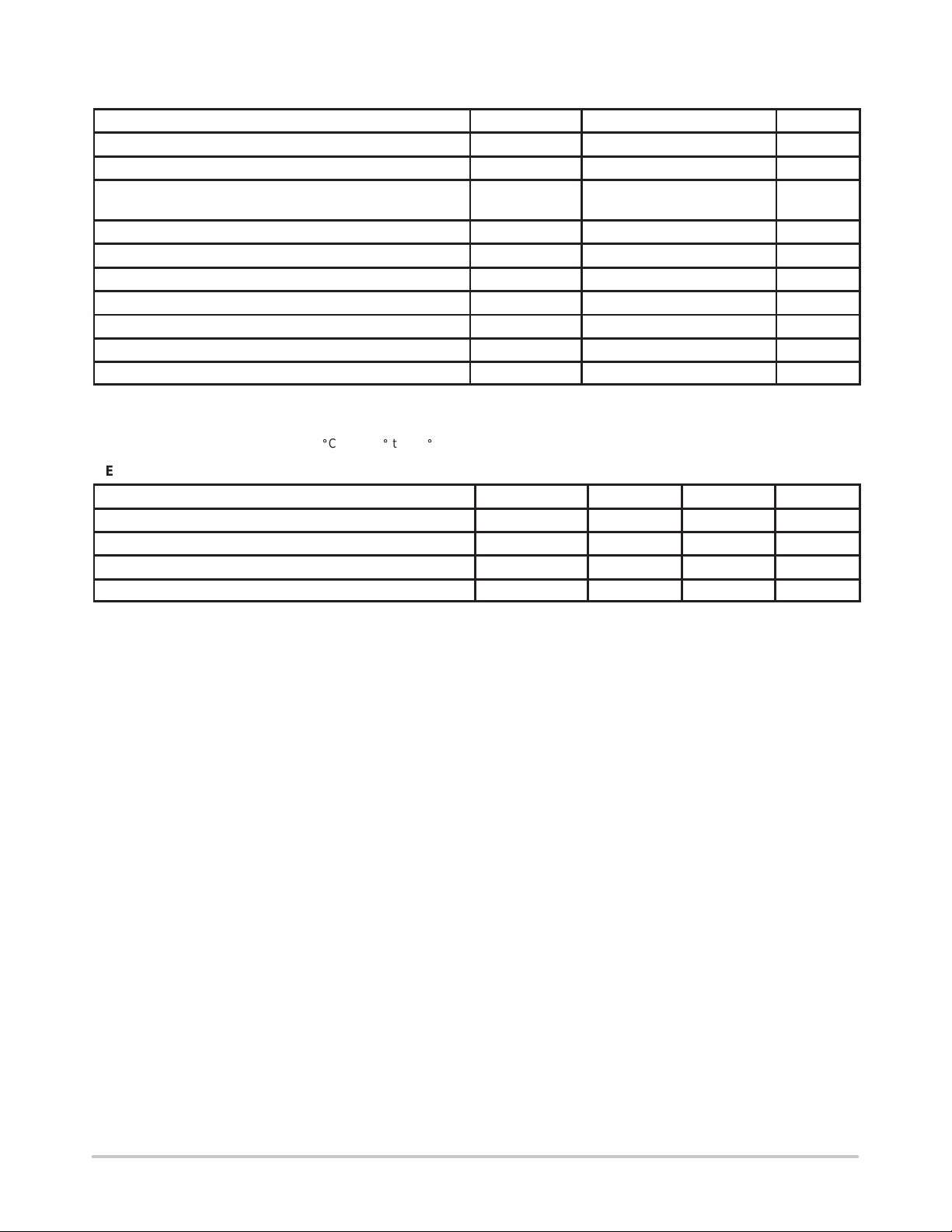
MAXIMUM RATINGS*
Characteristics Symbol Value Unit
DC Supply Voltage V
DC Input Voltage V
DC Output Voltage VCC = 0
Input Diode Current I
Output Diode Current (V
DC Output Current, per Pin I
DC Supply Current, VCC and GND I
Power dissipation in still air, SC–88A † P
Lead temperature, 1 mm from case for 10 s T
Storage temperature T
* Maximum Ratings are those values beyond which damage to the device may occur. Exposure to these conditions or conditions beyond those
indicated may adversely affect device reliability. Functional operation under absolute–maximum–rated conditions is not implied. Functional
operation should be restricted to the Recommended Operating Conditions.
†Derating — SC–88A Package: –3 mW/_C from 65_ to 125_C
High or Low State
< GND; V
OUT
> VCC) I
OUT
V
OUT
CC
IN
OUT
IK
OK
CC
D
L
stg
RECOMMENDED OPERATING CONDITIONS
Characteristics Symbol Min Max Unit
DC Supply Voltage V
DC Input Voltage V
DC Output Voltage V
Operating Temperature Range T
CC
IN
OUT
A
–0.5 to +7.0 V
–0.5 to +7.0 V
–0.5 to 7.0
–0.5 to VCC + 0.5
–20 mA
+20 mA
+25 mA
+50 mA
200 mW
260 °C
–65 to +150 °C
4.5 5.5 V
0.0 5.5 V
0.0 V
–55 +85 °C
CC
V
V
http://onsemi.com
2
MC74VHC1G14
Î
Î
Î
Î
Î
Î
Î
Î
Î
Î
A to Y
Î
Î
Î
Î
Î
Î
Î
DC ELECTRICAL CHARACTERISTICS
V
CC
Symbol Parameter Test Conditions (V) Min Typ Max Min Max Min Max Unit
V
T+
Positive Threshold
Voltage
3.0
4.5
5.5
V
T–
Negative Threshold
Voltage
3.0
4.5
5.5
V
H
Hysteresis Voltage 3.0
4.5
5.5
V
OH
Minimum High–Level
Output Voltage
VIN = VIH or V
IOH = –50µA
IL
IOH = –50µA
IOH = –4mA
IOH = –8mA
V
OL
Maximum Low–Level
Output Voltage
VIN = VIH or V
IOL = 50µA
IL
2.0
3.0
4.5
3.0
4.5
2.0
3.0
4.5
I
I
IN
CC
Maximum Input
Leakage Current
Maximum Quiescent
Supply Current
IOL = 4mA
IOL = 8mA
VIN = 5.5V or GND 0 to
VIN = VCC or GND 5.5 2.0 20 40 µA
3.0
4.5
5.5
TA = 25°C TA ≤ 85°C TA ≤ 125°C
1.85
2.86
3.50
1.35
1.65
0.30
0.40
0.50
2.58
3.94
0.9
1.9
2.9
4.4
2.0
3.0
3.6
1.5
2.3
2.9
0.57
0.67
0.74
2.0
3.0
4.5
0.0
0.0
0.0
2.20
3.15
3.85
1.65
2.46
3.05
1.20
1.40
1.60
0.1
0.1
0.1
0.36
0.36
0.9
1.35
1.65
0.30
0.40
0.50
1.9
2.9
4.4
2.48
3.80
2.20
3.15
3.85
1.20
1.40
1.60
0.1
0.1
0.1
0.44
0.44
±0.1 ±1.0 ±1.0 µA
0.9
1.35
1.65
0.30
0.40
0.50
1.9
2.9
4.4
2.34
3.66
2.20
3.15
3.85
1.20
1.40
1.60
0.1
0.1
0.1
0.52
0.52
V
V
V
V
V
V
V
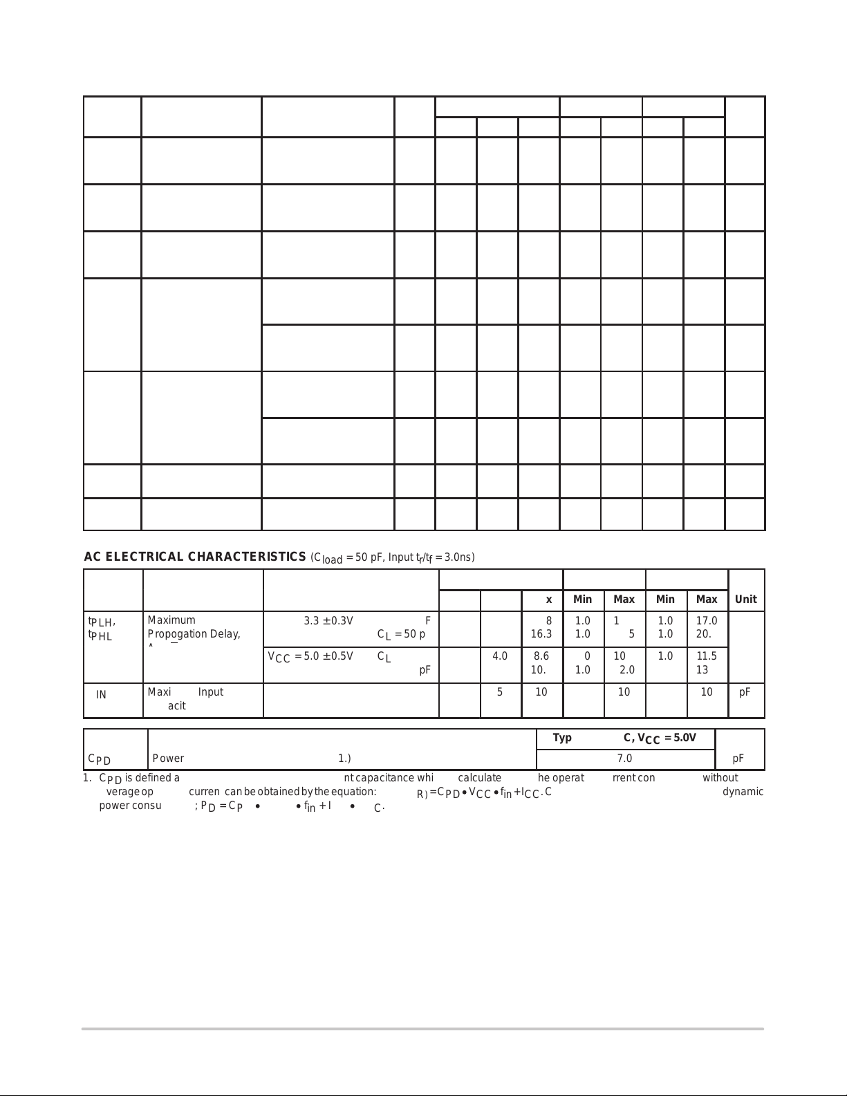
AC ELECTRICAL CHARACTERISTICS (C
Symbol
t
,
PLH
ÎÎ
t
PHL
ÎÎÎООООО
C
IN
Parameter
Maximum
ООООО
Propogation Delay,
Maximum Input
Capacitance
VCC = 3.3 ± 0.3V CL = 15 pF
ООООООО
VCC = 5.0 ± 0.5V CL = 15 pF
ООООООО
= 50 pF, Input tr/tf = 3.0ns)
load
Test Conditions
CL = 50 pF
CL = 50 pF
TA = 25°C
Min
Typ
7.0
ÎÎÎ
8.5
4.0
ÎÎÎ
5.5
5
Max
12.8
Î
16.3
8.6
10.6
Î
10
TA ≤ 85°C
Min
1.0
Î
1.0
1.0
1.0
Î
Max
15.0
Î
18.5
10.0
12.0
Î
10
TA ≤ 125°C
Min
Max
1.0
17.0
Î
1.0
20.5
1.0
11.5
1.0
13.5
Î
Î
Î
10
Unit
ns
pF
Typical @ 25°C, VCC = 5.0V
C
PD
Power Dissipation Capacitance (Note 1.)
7.0
pF
1. CPD is defined as the value of the internal equivalent capacitance which is calculated from the operating current consumption without load.
Average operating current can be obtained by the equation: I
2
power consumption; PD = CPD V
fin + ICC VCC.
CC
CC(OPR
= CPD VCC fin + ICC. CPD is used to determine the no–load dynamic
)
http://onsemi.com
3
 Loading...