

MOTOROLA MC74VHC138MEL, MC74VHC138ML1, MC74VHC138ML2, MC74VHC138N, MC74VHC138DTEL Datasheet
...
SEMICONDUCTOR TECHNICAL DATA
1
REV 1
Motorola, Inc. 1997
6/97
The MC74VHC138 is an advanced high speed CMOS 3–to–8 decoder
fabricated with silicon gate CMOS technology. It achieves high speed
operation similar to equivalent Bipolar Schottky TTL while maintaining
CMOS low power dissipation.
When the device is enabled, three Binary Select inputs (A0 – A2)
determine which one of the outputs (Y0
– Y7) will go Low. When enable input
E3 is held Low or either E2
or E1 is held High, decoding function is inhibited
and all outputs go high. E3, E2
, and E1 inputs are provided to ease cascade
connection and for use as an address decoder for memory systems.
The internal circuit is composed of three stages, including a buffer output
which provides high noise immunity and stable output. The inputs tolerate
voltages up to 7V, allowing the interface of 5V systems to 3V systems.
• High Speed: tPD = 5.7ns (Typ) at VCC = 5V
• Low Power Dissipation: ICC = 4µA (Max) at TA = 25°C
• High Noise Immunity: V
NIH
= V
NIL
= 28% V
CC
• Power Down Protection Provided on Inputs
• Balanced Propagation Delays
• Designed for 2V to 5.5V Operating Range
• Low Noise: V
OLP
= 0.8 V (Max)
• Pin and Function Compatible with Other Standard Logic Families
• Latchup Performance Exceeds 300mA
• ESD Performance: HBM > 2000V; Machine Model > 200V
• Chip Complexity: 122 FETs or 30.5 Equivalent Gates
7
Y6
Y5
Y4
Y3
Y2
Y1
Y0
Y7
9
10
11
12
13
14
15
3
2
1
E3
E2
A0
A1
A2
ACTIVE–LOW
OUTPUTS
SELECT
INPUTS
E1
ENABLE
INPUTS
4
5
6
Inputs Outputs
E3 E2
E1 A2 A1 A0 Y0 Y1 Y2 Y3 Y4 Y5 Y6 Y7
X X H XXXHHHHHHHH
X H X XXXHHHHHHHH
L X X XXXHHHHHHHH
H L L LLLLHHHHHHH
H L L LLHHLHHHHHH
H L L LHLHHLHHHHH
H L L LHHHHHLHHHH
H L L HLLHHHHLHHH
H L L HLHHHHHHLHH
H L L HHLHHHHHHLH
H L L HHHHHHHHHHL
FUNCTION TABLE
H = high level (steady state); L = low level (steady state);
X = don’t care
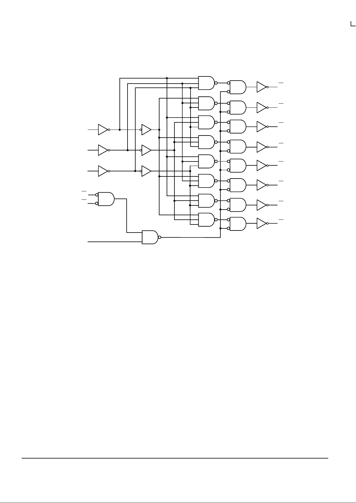
LOGIC DIAGRAM
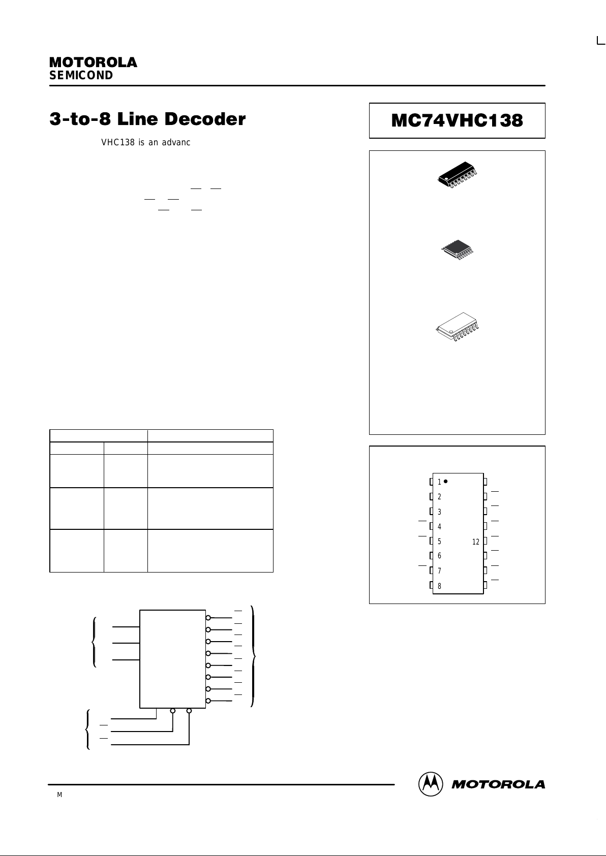
PIN ASSIGNMENT
13
14
15
16
9
10
11
12
5
4
3
2
1
8
7
6
A0
E1
A2
A1
Y7
E3
E2
GND
Y3
Y2
Y1
Y0
V
CC
Y5
Y4
Y6
D SUFFIX
16–LEAD SOIC PACKAGE
CASE 751B–05
DT SUFFIX
16–LEAD TSSOP PACKAGE
CASE 948F–01
ORDERING INFORMATION
MC74VHCXXXD
MC74VHCXXXDT
MC74VHCXXXM
SOIC
TSSOP
SOIC EIAJ
M SUFFIX
16–LEAD SOIC EIAJ PACKAGE
CASE 966–01
MC74VHC138
MOTOROLA VHC Data – Advanced CMOS Logic
DL203 — Rev 1
2
A0
A1
A2
E2
E1
E3
1
2
3
4
5
6
15
14
13
12
11
10
9
7
Y1
Y2
Y3
Y4
Y5
Y6
Y7
Y0
EXPANDED LOGIC DIAGRAM
MC74VHC138
VHC Data – Advanced CMOS Logic
DL203 — Rev 1
3 MOTOROLA
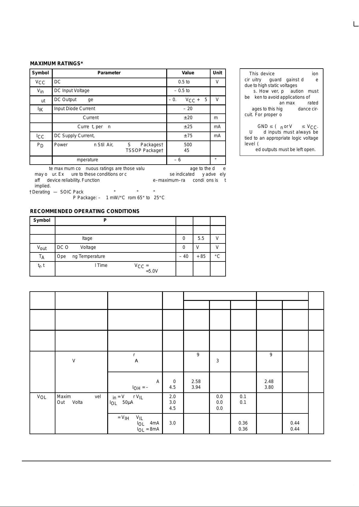
MAXIMUM RATINGS*
Symbol
Parameter
Value
Unit
V
CC
DC Supply Voltage
– 0.5 to + 7.0
V
V
in
DC Input Voltage
– 0.5 to + 7.0
V
V
out
DC Output Voltage
– 0.5 to VCC + 0.5
V
I
IK
Input Diode Current
– 20
mA
I
OK
Output Diode Current
± 20
mA
I
out
DC Output Current, per Pin
± 25
mA
I
CC
DC Supply Current, VCC and GND Pins
± 75
mA
Î
Î
P
D
ОООООООООООО
Î
Power Dissipation in Still Air, SOIC Packages†
TSSOP Package†
ÎÎÎÎ
Î
500
450
Î
Î
mW
T
stg
Storage Temperature
– 65 to + 150
_
C
* Absolute maximum continuous ratings are those values beyond which damage to the device
may occur. Exposure to these conditions or conditions beyond those indicated may adversely
affect device reliability . Functional operation under absolute–maximum–rated conditions is not
implied.
†Derating — SOIC Packages: – 7 mW/_C from 65_ to 125_C
TSSOP Package: – 6.1 mW/_C from 65_ to 125_C
RECOMMENDED OPERATING CONDITIONS
Symbol
Parameter
Min
Max
Unit
V
CC
DC Supply Voltage
2.0
5.5
V
V
in
DC Input Voltage
0
5.5
V
V
out
DC Output Voltage
0
V
CC
V
T
A
Operating Temperature
– 40
+ 85
_
C
tr, t
f
Input Rise and Fall Time VCC = 3.3V ±0.3V
VCC =5.0V ±0.5V00
10020ns/V
DC ELECTRICAL CHARACTERISTICS
ÎÎÎ
V
TA = 25°C
TA = – 40 to 85°C
Symbol
Parameter
Test Conditions
ÎÎÎ
V
CC
V
Min
Typ
Max
Min
Max
Unit
ÎÎ
Î
V
IH
ÎÎÎÎ
Î
Minimum High–Level
Input Voltage
ОООООО
Î
ÎÎÎ
ÎÎ
Î
2.0
3.0 to
5.5
ÎÎ
Î
1.50
VCC x 0.7
ÎÎÎÎÎÎÎ
Î
1.50
VCC x 0.7
ÎÎ
Î
V
ÎÎ
Î
ÎÎ
Î
V
IL
ÎÎÎÎ
Î
ÎÎÎÎ
Î
Maximum Low–Level
Input Voltage
ОООООО
Î
ОООООО
Î
ÎÎÎ
ÎÎ
Î
ÎÎ
Î
2.0
3.0 to
5.5
ÎÎ
Î
ÎÎ
Î
Î
Î
Î
Î
ÎÎ
Î
ÎÎ
Î
0.50
VCC x 0.3
ÎÎ
Î
ÎÎ
Î
ÎÎ
Î
ÎÎ
Î
0.50
VCC x 0.3
V
ÎÎ
Î
ÎÎ
Î
V
OH
ÎÎÎÎ
Î
ÎÎÎÎ
Î
Minimum High–Level
Output Voltage
ОООООО
Î
ОООООО
Î
Vin = VIH or V
IL
IOH = – 50µ
A
ÎÎÎ
ÎÎ
Î
ÎÎ
Î
2.0
3.0
4.5
ÎÎ
Î
ÎÎ
Î
1.9
2.9
4.4
Î
Î
Î
Î
2.0
3.0
4.5
ÎÎ
Î
ÎÎ
Î
ÎÎ
Î
ÎÎ
Î
1.9
2.9
4.4
ÎÎ
Î
ÎÎ
Î
V
ÎÎÎÎÎÎÎÎОООООО
Î
Vin = VIH or V
IL
IOH = – 4mA
IOH = – 8mA
ÎÎÎ
ÎÎ
Î
3.0
4.5
ÎÎ
Î
2.58
3.94
ÎÎÎÎÎÎÎ
Î
2.48
3.80
ÎÎ
Î
ÎÎ
Î
ÎÎ
V
OL
ÎÎÎÎ
Î
ÎÎÎÎ
Maximum Low–Level
Output Voltage
ОООООО
Î
ОООООО
Vin = VIH or V
IL
IOL = 50µA
ÎÎÎ
ÎÎ
Î
ÎÎ
2.0
3.0
4.5
ÎÎ
Î
ÎÎ
Î
Î
Î
0.0
0.0
0.0
ÎÎ
Î
ÎÎ
0.1
0.1
0.1
ÎÎ
Î
ÎÎ
ÎÎ
Î
ÎÎ
0.1
0.1
0.1
V
ÎÎ
Î
ÎÎ
Î
ÎÎÎÎ
Î
ÎÎÎÎ
Î
ОООООО
Î
ОООООО
Î
Vin = VIH or V
IL
IOL = 4mA
IOL = 8mA
ÎÎÎ
ÎÎ
Î
ÎÎ
Î
3.0
4.5
ÎÎ
Î
ÎÎ
Î
Î
Î
Î
Î
ÎÎ
Î
ÎÎ
Î
0.36
0.36
ÎÎ
Î
ÎÎ
Î
ÎÎ
Î
ÎÎ
Î
0.44
0.44
This device contains protection
circuitry to guard against damage
due to high static voltages or electric
fields. However, precautions must
be taken to avoid applications of any
voltage higher than maximum rated
voltages to this high–impedance circuit. For proper operation, Vin and
V
out
should be constrained to the
range GND v (Vin or V
out
) v VCC.
Unused inputs must always be
tied to an appropriate logic voltage
level (e.g., either GND or VCC).
Unused outputs must be left open.
 Loading...