

Motorola MC74LCX2952DW, MC74LCX2952SD, MC74LCX2952DT Datasheet
SEMICONDUCTOR TECHNICAL DATA
&-&$* *$
")*( (%)",( "*!
+$ +*'+* % $&#
%$)
"*! &$(%* %'+*) % +*'+*)
** &%%,(*"%
The MC74LCX2952 is a high performance, non–inverting octal
registered transceiver operating from a 2.7 to 3.6V supply. High
impedance TTL compatible inputs significantly reduce current loading to
input drivers while TTL compatible outputs offer improved switching noise
performance. A VI specification of 5.5V allows MC74LCX2952 inputs to
be safely driven from 5V devices. The MC74LCX2952 is suitable for
memory address driving and all TTL level bus oriented transceiver
applications.
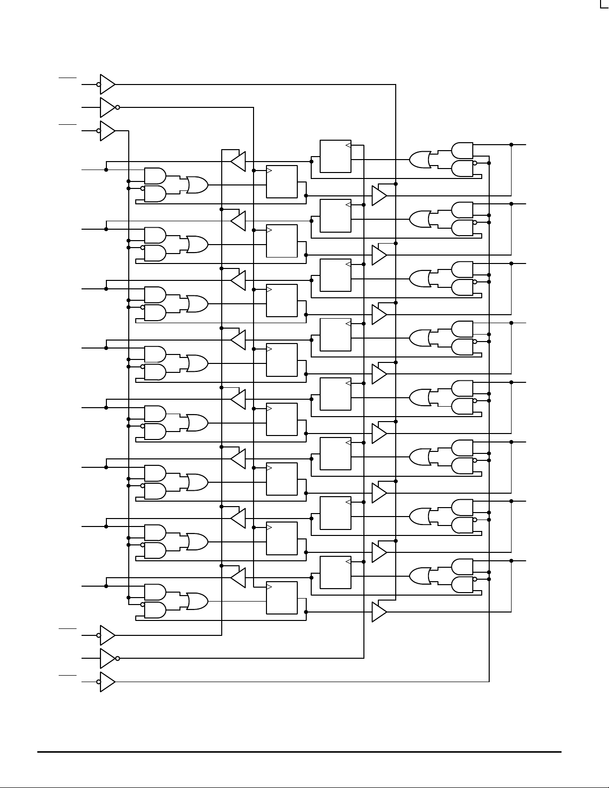
Two 8–bit back to back registers store data from either of two
bidirectional buses. Data applied to the inputs is entered and stored on
the rising edge of the Clock (CAB, CBA) provided that the Clock Enable
(CEAB
, CEBA) is Low. The data is then presented at the 3–state output
buffers, but is only accessible when the Output Enable (OEAB
Low. The operation of the MC74LCX2952 is symmetrical — A inputs to B
outputs occurs in the same manner as B inputs to A outputs.
, OEBA) is
LOW–VOLTAGE CMOS
OCTAL REGISTERED
TRANSCEIVER
DW SUFFIX
24–LEAD PLASTIC SOIC WIDE PACKAGE
CASE 751E–04
• Designed for 2.7 to 3.6V V
Operation
CC
• 5V Tolerant — Interface Capability With 5V TTL Logic
• Supports Live Insertion and Withdrawal
• I
Specification Guarantees High Impedance When VCC = 0V
OFF
• LVTTL Compatible
• LVCMOS Compatible
• 24mA Balanced Output Sink and Source Capability
• Near Zero Static Supply Current in All Three Logic States (10µA)
Substantially Reduces System Power Requirements
• Latchup Performance Exceeds 500mA
• ESD Performance: Human Body Model >2000V; Machine Model >200V
V
A7 A6 A5 A4 A3 A2 A1 A0 OEBA
CC
2324 22 21 20 19 18
21 34567
B7 B6 B5 B4 B3 B2 B1 B0 OEAB CAB
Figure 1. 24–Lead Pinout (Top View)
17
16
9
8
15
10
CEAB GND
CBA CEBA
14
13
11
12
24–LEAD PLASTIC SSOP PACKAGE
24–LEAD PLASTIC TSSOP PACKAGE
PIN NAMES
Pins
A0–A7
B0–B7
CAB, CBA
CEAB
, CEBA
OEAB, OEBA
SD SUFFIX
CASE 940D–03
DT SUFFIX
CASE 948H–01
Function
Side A Inputs/Outputs
Side B Inputs/Outputs
Clock Pulse Inputs
Clock Enable Inputs
Output Enable Inputs
3/97
Motorola, Inc. 1997
1
REV 1
MC74LCX2952
9
OEAB
10
CAB
11
CEAB
16
A0
17
A1
18
A2
19
A3
20
A4
21
A5
22
A6
23
A7
8
C
Q
C
Q
D
C
Q
D
C
Q
D
C
Q
D
C
Q
D
C
Q
D
C
Q
D
C
Q
D
D
C
Q
D
C
Q
D
C
Q
D
C
Q
D
C
Q
D
C
Q
D
C
Q
D
B0
7
B1
6
B2
5
B3
4
B4
3
B5
2
B6
1
B7
15
OEBA
14
CBA
13
CEBA
Figure 2. Logic Diagram
MOTOROLA LCX DATA
2
BR1339 — REV 3
MC74LCX2952
O
FUNCTION TABLE
Inputs
OEAB OEBA CEAB CEBA CAB CBA An Bn
H H Input Input
l l ↑ ↑ X X Load Register; Disable Outputs
↑ ↑ X X Hold; Disable Outputs
h h X X X X Hold; Disable Outputs
L H Input Output
l X ↑ X l
↑ X X QA Hold; Read B Output
h X X X X QA Hold; Read B Output
H L Output Input
X l X ↑ L
X ↑ QB X Hold; Read A Output
X h X X QB X Hold; Read A Output
H = High Voltage Level; h = High Voltage Level One Setup Time Prior to the Low–to–High Clock Transition; L = Low Voltage Level; l = Low Voltage Level One Setup
Time Prior to the Low–to–High Clock T ransition; X = Don’t Care; ↑ = Low–to–High Clock Transition; ↑
QB = B input storage register; * = The clocks are not internally gated with either the Output Enables or the Source Inputs. Therefore, data at the A or B ports may be
clocked into the storage registers, at any time. For ICC reasons, Do Not Float Inputs.
Data Ports
h
H
perating Mode
L
H
l
h
= NOT Low–to–High Clock Transition; QA = A input storage register;
Load A to B Register; Read B Output
Load B to A Register; Read A Output
ABSOLUTE MAXIMUM RATINGS*
Symbol Parameter Value Condition Unit
V
CC
V
I
V
O
I
IK
I
OK
I
O
I
CC
I
GND
T
STG
* Absolute maximum continuous ratings are those values beyond which damage to the device may occur. Exposure to these conditions or
conditions beyond those indicated may adversely affect device reliability. Functional operation under absolute–maximum–rated conditions is
not implied.
1. Output in HIGH or LOW State. IO absolute maximum rating must be observed.
DC Supply Voltage –0.5 to +7.0 V
DC Input Voltage –0.5 ≤ VI ≤ +7.0 V
DC Output Voltage –0.5 ≤ VO ≤ +7.0 Output in 3–State V
–0.5 ≤ VO ≤ VCC + 0.5 Note 1. V
DC Input Diode Current –50 VI < GND mA
DC Output Diode Current –50 VO < GND mA
+50 VO > V
DC Output Source/Sink Current ±50 mA
DC Supply Current Per Supply Pin ±100 mA
DC Ground Current Per Ground Pin ±100 mA
Storage Temperature Range –65 to +150 °C
CC
mA
LCX DATA
BR1339 — REV 3
3 MOTOROLA
 Loading...