

Motorola MC74LCX16646DT Datasheet
SEMICONDUCTOR TECHNICAL DATA
$+ $"( !(
&#'!*&!'(&
&#'!*&
!( $"&#( #%)(' # )(%)('
(( $##*&(!#
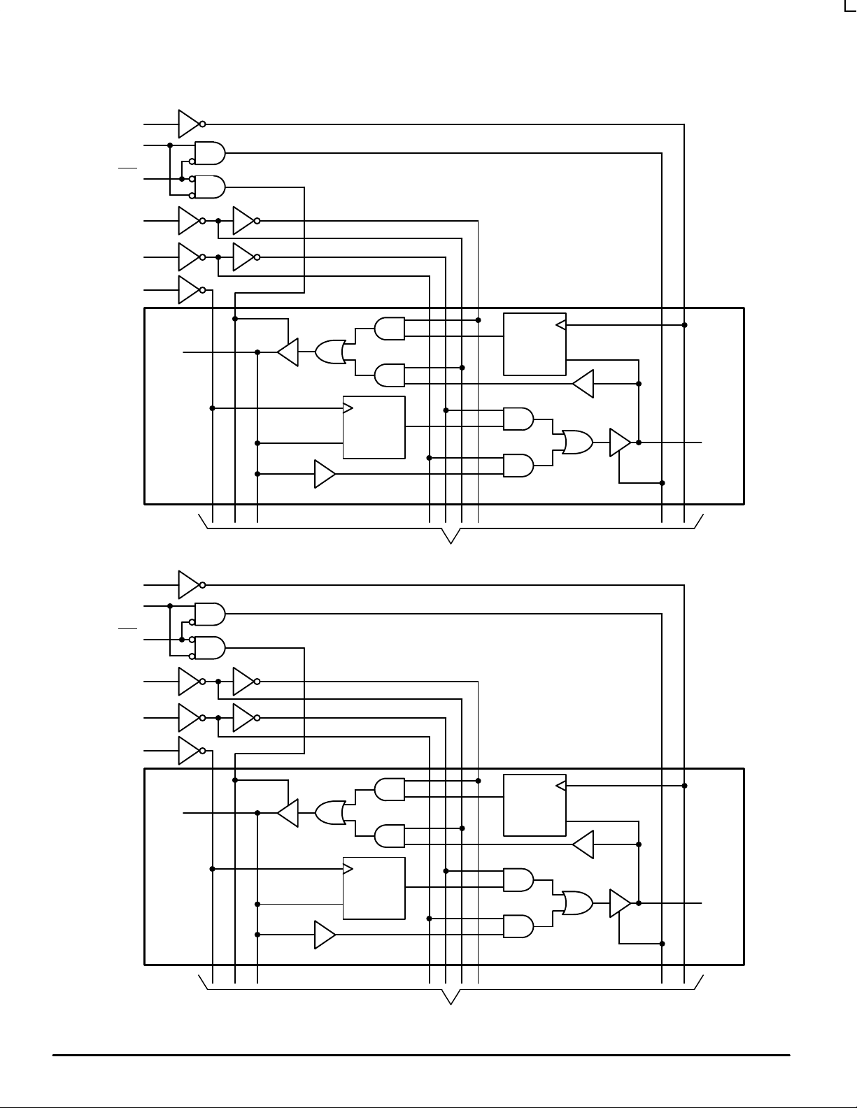
The MC74LCX16646 is a high performance, non–inverting 16–bit
transceiver/registered transceiver operating from a 2.7 to 3.6V supply.
The device is byte controlled. Each byte has separate control inputs
which can be tied together for full 16–bit operation. High impedance TTL
compatible inputs significantly reduce current loading to input drivers
while TTL compatible outputs offer improved switching noise
performance. A VI specification of 5.5V allows MC74LCX16646 inputs to
be safely driven from 5V devices. The MC74LCX16646 is suitable for
memory address driving and all TTL level bus oriented transceiver
applications.
Data on the A or B bus will be clocked into the registers as the
appropriate clock pin goes from a LOW–to–HIGH logic level. Output
Enable (OEn
the transceiver outputs. In the transceiver mode, data present at the high
impedance port may be stored in either the A or the B register or in both.
The select controls (SBAn, SABn) can multiplex stored and real–time
(transparent mode) data. The DIR determines which bus will receive data
when OE
stored in the B register or B data may be stored in the A register. Only one
of the two buses, A or B, may be driven at one time.
• Designed for 2.7 to 3.6V V
• 5.2ns Maximum t
) and Direction Control (DIRn) pins are provided to control
is active LOW. In the isolation mode (OE HIGH), A data may be
Operation
CC
pd
• 5V Tolerant — Interface Capability With 5V TTL Logic
• Supports Live Insertion and Withdrawal
• I
Specification Guarantees High Impedance When VCC = 0V
OFF
• LVTTL Compatible
• LVCMOS Compatible
• 24mA Balanced Output Sink and Source Capability
• Near Zero Static Supply Current in All Three Logic States (20µA)
Substantially Reduces System Power Requirements
• Latchup Performance Exceeds 500mA
• ESD Performance: Human Body Model >2000V; Machine Model >200V
LOW–VOLTAGE CMOS
16–BIT TRANSCEIVER/
REGISTERED TRANSCEIVER
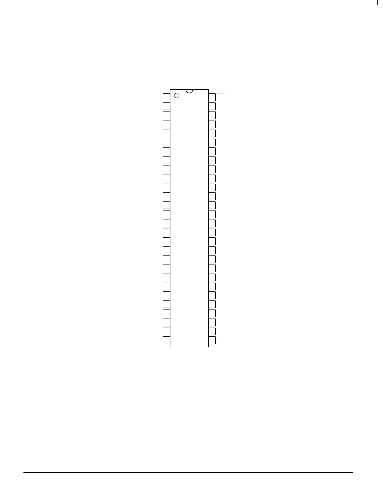
PLASTIC TSSOP PACKAGE
PIN NAMES
Pins
A0–A15
B0–B15
CABn, CBAn
SABn, SBAn
DIRn, OEn
DT SUFFIX
CASE 1202–01
Function
Side A Inputs/Outputs
Side B Inputs/Outputs
Clock Pulse Inputs
Select Control Inputs
Output Enable Inputs
This document contains information on a new product. Specifications and information herein are subject to
change without notice.
11/96
Motorola, Inc. 1996
1
REV 0.2
MC74LCX16646
DIR1
V
CC
A11
V
CC
SAB2
DIR2
OE1
561
CBA1CAB1
552
SBA1SAB1
543
GNDGND
534
B0A0
525
B1A1
516
V
507
CC
B2A2
498
B3A3
489
B4A4
4710
GNDGND
4611
B5A5
4512
B6A6
4413
B7A7
4314
B8A8
4215
B9A9
4116
B10A10
4017
GNDGND
3918
B11
3819
B12A12
3720
B13A13
3621
V
3522
CC
B14A14
3423
B15A15
3324
GNDGND
3225
SBA2
3126
CBA2CAB2
3027
OE2
2928
MOTOROLA LCX DATA
2
BR1339 — REV 3
MC74LCX16646
CBA1
DIR1
OE1
SBA1
SAB1
CAB1
55
1
56
54
3
2
A0:7
1 of 8 Channels
LOGIC DIAGRAM
C
Q
D
C
Q
D
B0:7
CBA2
DIR2
OE2
SBA2
SAB2
CAB2
30
28
29
31
26
27
A8:15
1 of 8 Channels
To 7 Other Channels
C
Q
D
C
Q
D
B8:15
LCX DATA
BR1339 — REV 3
To 7 Other Channels
3 MOTOROLA
 Loading...