

Motorola MC74LCX16543DT Datasheet

SEMICONDUCTOR TECHNICAL DATA
#*#!' '
' " %"& )%
' #!%"' "$('& " ('$('&
'' #"")%' "
The MC74LCX16543 is a high performance, non–inverting 16–bit
latching transceiver operating from a 2.7 to 3.6V supply. The device is
byte controlled. Each byte has separate control inputs which can be tied
together for full 16–bit operation. High impedance TTL compatible inputs
significantly reduce current loading to input drivers while TTL compatible
outputs offer improved switching noise performance. A VI specification of
5.5V allows MC74LCX16543 inputs to be safely driven from 5V devices.
The MC74LCX16543 is suitable for memory address driving and all TTL
level bus oriented transceiver applications.
For data flow from A to B with the EAB
Enable (OEAB
indicated in the Function Table. With EAB
A–to–B Latch Enable (LEAB
transparent; a subsequent LOW–to–HIGH transition of the LEAB
will latch the A latches, and the outputs no longer change with the A
inputs. With EAB
active and reflect the data present at the output of the A latches. Control
of data flow from B to A is symetric to that above, but uses the EBA
, and OEBA inputs.
LEBA
) must be LOW in order to enable data to the B bus, as
) input makes the A–to–B latches
and OEAB both LOW, the 3–State B output buf fers are
LOW, the A–to–B Output
LOW, a LOW signal on the
signal
LOW–VOLTAGE CMOS
16–BIT LATCHING
TRANSCEIVER
,
PLASTIC TSSOP PACKAGE
DT SUFFIX
CASE 1202–01
• Designed for 2.7 to 3.6V V
• 5.2ns Maximum t
pd
Operation
CC
• 5V T olerant — Interface Capability With 5V TTL Logic
• Supports Live Insertion and Withdrawal
• I
• LVTTL Compatible
Specification Guarantees High Impedance When VCC = 0V
OFF
PIN NAMES
• LVCMOS Compatible
• 24mA Balanced Output Sink and Source Capability
• Near Zero Static Supply Current in All Three Logic States (20µA)
Substantially Reduces System Power Requirements
• Latchup Performance Exceeds 500mA
• ESD Performance: Human Body Model >2000V; Machine Model >200V
This document contains information on a new product. Specifications and information herein are subject to
change without notice.
Pins
OExxn
Exxn
LExxn
A0–A15
B0–B15
Function
Output Enable Inputs
Enable Inputs
Latch Enable Inputs
3–State Inputs/Outputs
3–State Inputs/Outputs
11/96
Motorola, Inc. 1996
1
REV 0.2
MC74LCX16543
A0
OEBA1
EBA1
LEBA1
A8
OEBA2
EBA2
LEBA2
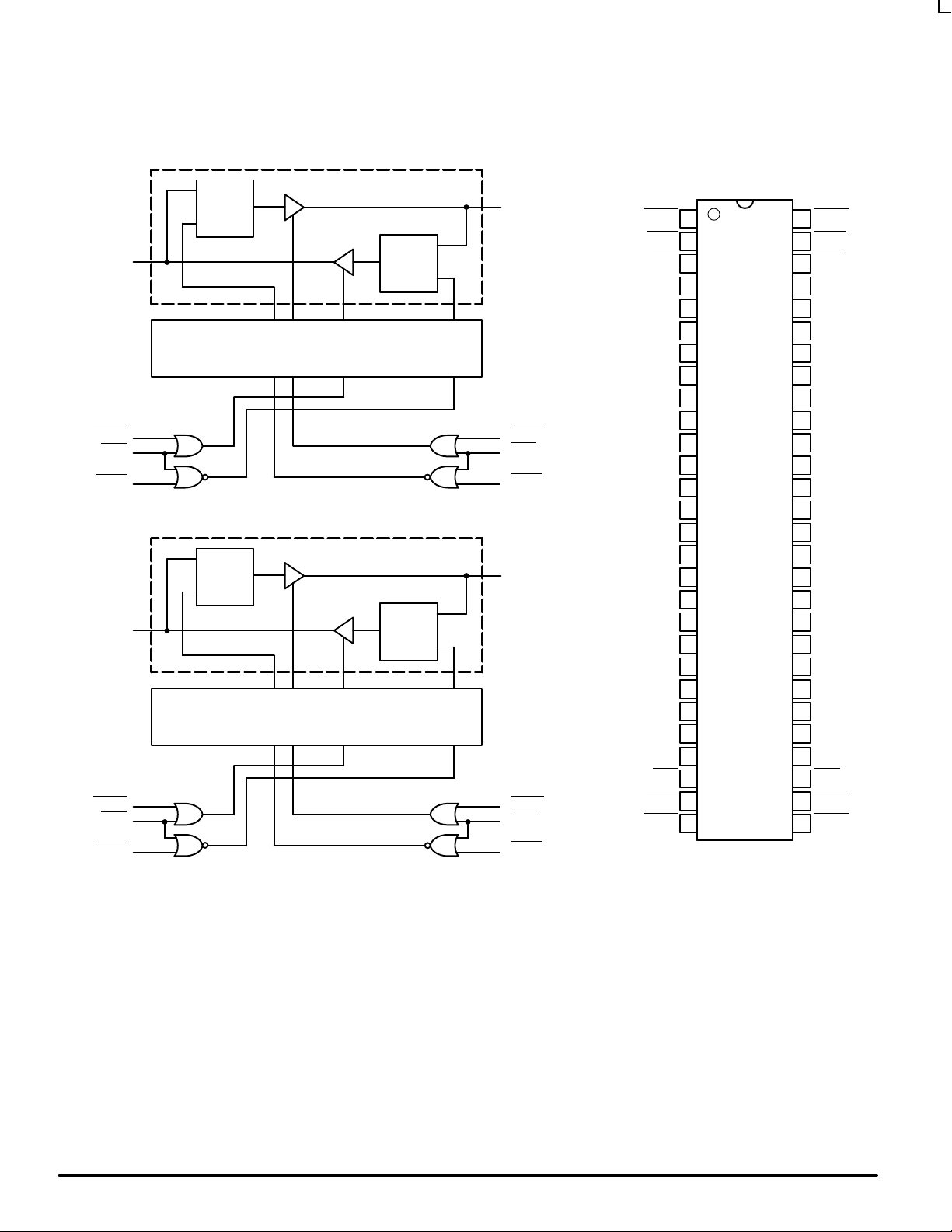
LOGIC DIAGRAM
D
Q
LE
5
DETAIL A x 7
56 1
54
55
D
Q
LE
15
DETAIL Bx 7
29 28
31
30
DETAIL A
D
Q
LE
DETAIL B
D
Q
LE
Pinout: 56-Lead TSSOP
(Top View)
52
B0
OEAB1
EAB1
3
LEAB1
2
42
B8
OEAB2
EAB2
26
LEAB2
27
OEAB1
LEAB1
EAB1
A0
V
CC
A5
A11
V
CC
EAB2
LEAB2
OEAB2
561
552
543
534
525
516
507
498
489
4710
4611
4512
4413
4314
4215
4116
4017
3918
3819
3720
3621
3522
3423
3324
3225
3126
3027
2928
OEBA1
LEBA1
EBA1
GNDGND
B0
B1A1
V
CC
B2A2
B3A3
B4A4
GNDGND
B5
B6A6
B7A7
B8A8
B9A9
B10A10
GNDGND
B11
B12A12
B13A13
V
CC
B14A14
B15A15
GNDGND
EBA2
LEBA2
OEBA2
MOTOROLA LCX DATA
2
BR1339 — REV 3

MC74LCX16543
O
FUNCTION TABLE
Inputs
OEABn OEBAn EABn EBAn LEABn LEBAn An Bn
H H Input Input
X X X X X X Disable Outputs
L L L L X X Transparent Data; Outputs Disabled
H H l
L H Input Output
H X* L X l
H X X Z Hold; B Outputs Disabled
L X* L X L
H X l
H L Output Input
X* H X L Z
X H Z X Hold; A Outputs DIsabled
X* L X L L
X H L
H = High Voltage Level; h = High Voltage Level One Setup T ime Prior to the Latch Enable or Enable Low–to–High Transition; L = Low Voltage Level;
l = Low Voltage Level One Setup Time Prior to the Latch Enable or Enable Low–to–High T ransition; X = Don’t Care; * = The latches are not internally
gated with the Output Enables. Therefore, data at the A or B ports may enter the latches at any time, provided that the LExx
accordingly. For ICC reasons, Do Not Float Inputs.
Data Ports
h
h
H
h
Z
H
H
perating Mode
l
h
Z
Z
L
H
L
H
l
h
L
H
l
h
Latch and Outputs Disabled
Load and B Outputs Disabled
Transparent A to B
Latch and Display B Outputs
Load and A Outputs Disabled
Transparent B to A
Latch and Display A Outputs
and Exx pins are set
ABSOLUTE MAXIMUM RATINGS*
Symbol Parameter Value Condition Unit
V
CC
V
I
V
O
I
IK
I
OK
I
O
I
CC
I
GND
T
STG
* Absolute maximum continuous ratings are those values beyond which damage to the device may occur. Exposure to these conditions or conditions
beyond those indicated may adversely affect device reliability. Functional operation under absolute–maximum–rated conditions is not implied.
1. Output in HIGH or LOW State. IO absolute maximum rating must be observed.
DC Supply Voltage –0.5 to +7.0 V
DC Input Voltage –0.5 ≤ VI ≤ +7.0 V
DC Output Voltage –0.5 ≤ VO ≤ +7.0 Output in 3–State V
–0.5 ≤ VO ≤ VCC + 0.5 Note 1. V
DC Input Diode Current –50 VI < GND mA
DC Output Diode Current –50 VO < GND mA
+50 VO > V
DC Output Source/Sink Current ±50 mA
DC Supply Current Per Supply Pin ±100 mA
DC Ground Current Per Ground Pin ±100 mA
Storage Temperature Range –65 to +150 °C
CC
mA
LCX DATA
BR1339 — REV 3
3 MOTOROLA
 Loading...