

Motorola MC74LCX16500DT Datasheet
SEMICONDUCTOR TECHNICAL DATA
&-&$*! #*
%#, ()$ +) (%) #, (
#*" &$ (%* %'+*) % +*'+*)
** &%%, (*#%!
The MC74LCX16500 is a high performance, non–inverting 18–bit
universal bus transceiver operating from a 2.7 to 3.6V supply. This part is
not byte controlled; it is “18–bit” controlled. High impedance TTL
compatible inputs significantly reduce current loading to input drivers
while TTL compatible outputs offer improved switching noise
performance. A VI specification of 5.5V allows MC74LCX16500 inputs to
be safely driven from 5V devices. The MC74LCX16500 is suitable for
memory address driving and all TTL level bus oriented transceiver
applications.
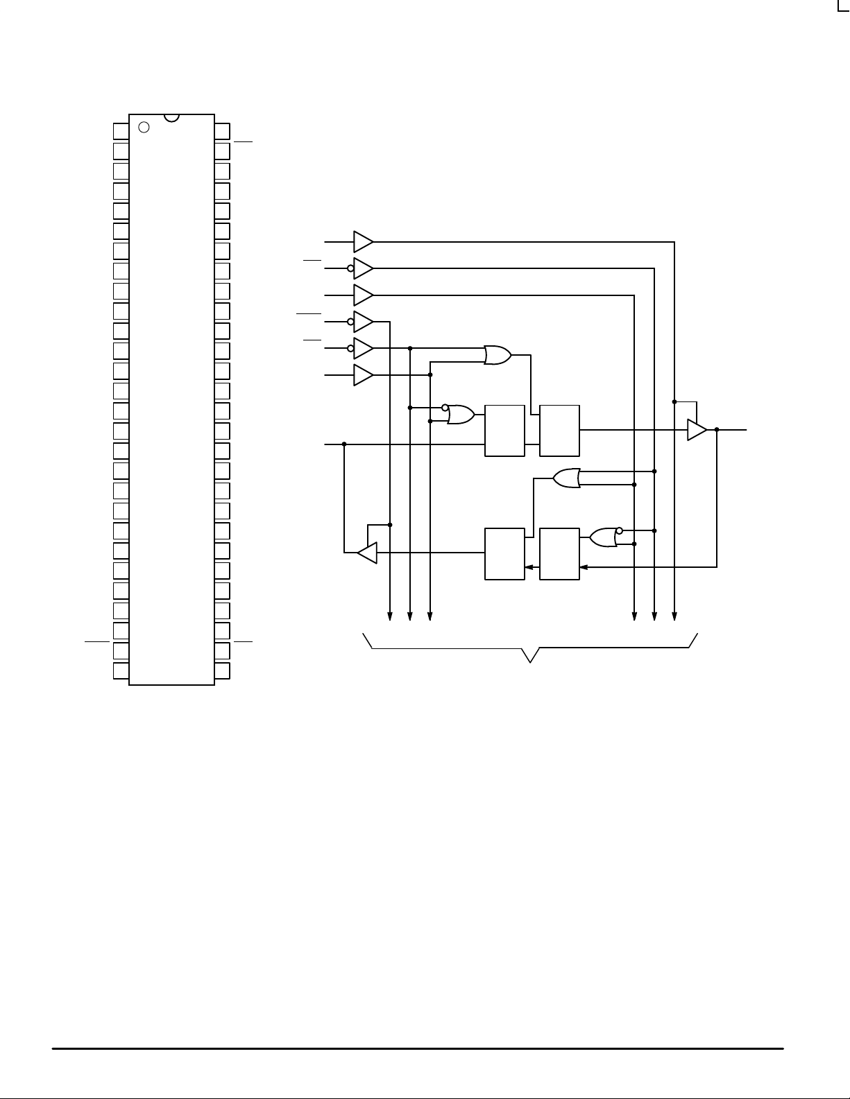
Data flow in each direction is controlled by Output Enable (OEAB,
OEBA
), Latch Enable (LEAB, LEBA) and Clock inputs (CAB, CBA). When
LEAB is HIGH, the A–to–B dataflow is transparent. When LEAB is LOW,
and CAB
HIGH–to–LOW transition of CAB
latch/flip–flop. The outputs are active when OEAB is HIGH. When OEAB
is LOW the B–outputs are in 3–state. Similarly , the LEBA, OEBA
control the B–to–A dataflow. Please note that the output enables are
complementary; OEAB is active HIGH, OEBA
• Designed for 2.7 to 3.6V V
• 6ns Maximum t
• 5V T olerant — Interface Capability With 5V TTL Logic
• Supports Live Insertion and Withdrawal
• I
• LVTTL Compatible
• LVCMOS Compatible
• 24mA Balanced Output Sink and Source Capability
• Near Zero Static Supply Current in All Three Logic States (20µA)
• Latchup Performance Exceeds 500mA
• ESD Performance: Human Body Model >2000V; Machine
is held at LOW or HIGH, the data A is latched; on the
the A–data is stored in the
is active LOW.
Operation
CC
pd
Specification Guarantees High Impedance When VCC = 0V
OFF
Substantially Reduces System Power Requirements
Model >200V
and CBA
LOW–VOLTAGE CMOS
18–BIT UNIVERSAL BUS
TRANSCEIVER
56–LEAD PLASTIC TSSOP PACKAGE
PIN NAMES
Pins
OEAB, OEBA
CAB, CBA
LEAB, LEBA
A0–A17
B0–B17
DT SUFFIX
CASE 1202–01
Function
Output Enable Inputs
Clock Pulse Inputs
Latch Enable Inputs
Side A Inputs/Outputs
Side B Inputs/Outputs
3/97
Motorola, Inc. 1997
1
REV 1
MC74LCX16500
LEAB
V
CC
A8
V
CC
OEBA
GNDOEAB
561
CAB
552
B0A0
543
GNDGND
534
B1A1
525
B2A2
516
V
507
CC
B3A3
498
B4A4
489
B5A5
4710
GNDGND
4611
B6A6
4512
B7A7
4413
B8
4314
B9A9
4215
B10A10
4116
B11A11
4017
GNDGND
3918
B12A12
3819
B13A13
3720
B14A14
3621
V
3522
CC
B15A15
3423
B16A16
3324
GNDGND
3225
B17A17
3126
CBA
3027
GNDLEBA
2928
OEAB
CBA
LEBA
OEBA
CAB
LEAB
A0
1
30
28
27
55
2
C1
3
1D
C1
1D
C1
1D
C1
1D
54
B0
To 17 Other Channels
Figure 1. 56-Lead Pinout
Figure 2. Logic Diagram
(Top View)
MOTOROLA LCX DATA
2
BR1339 — REV 3

MC74LCX16500
O
FUNCTION TABLE
Inputs Data Ports
OEAB OEBA LEAB LEBA CAB CBA An Bn
L H Input Input
H or L H or L X X Hold Data; A and B Outputs Disabled
L L
H H Input Output
L X
H X X X*
L L Output Input
X L
X H X* X
H L Output Output
L L H or L H or L QB QA Stored A Data to B Bus; Stored B Data to A Bus
H = High Voltage Level; L = Low Voltage Level; h = High Voltage Level One Setup Time Prior to the Latch Enable or Clock High–to–Low Transition; l = Low Voltage
Level One Setup Time Prior to the Latch Enable or Clock High–to–Low T ransition; X = Don’t Care; ↓ = High–to–Low Clock T ransition; QA = A Input Storage Register;
QB = B Input Storage Register; * = The clocks are not internally gated with either the Output Enables or the Source Inputs. Therefore, data at the A or B ports may be
clocked into the storage registers, at any time. For ICC reasons, Do Not Float Inputs.
↓ ↓
H or L X* X QA Hold and Display B Data
↓ X*
X* H or L QB X Hold and Display A Data
X* ↓
l
h
l
h
L
H
L
H
L
H
l
Clock A and/or B Data; A and B Outputs Disabled
h
L
Clock A Data to B Bus; Store A Data
H
L
A Data to B Bus; (Transparent)
H
l
Clock B Data to A Bus; Store B Data
h
L
B Data to A Bus; (Transparent)
H
perating Mode
LCX DATA
BR1339 — REV 3
3 MOTOROLA
 Loading...