

Motorola MC74LCX16374DT, MC74LCX16374DTR2 Datasheet
SEMICONDUCTOR TECHNICAL DATA
$+ $"( !(
,% "!%"$%
!( $"&#( #%)(' # )(%)('
(( $##*&(!#
The MC74LCX16374 is a high performance, non–inverting 16–bit
D–type flip–flop operating from a 2.7 to 3.6V supply. The device is byte
controlled. Each byte has separate Output Enable and Clock Pulse
inputs. These control pins can be tied together for full 16–bit operation.
High impedance TTL compatible inputs significantly reduce current
loading to input drivers while TTL compatible outputs offer improved
switching noise performance. A VI specification of 5.5V allows
MC74LCX16374 inputs to be safely driven from 5V devices.
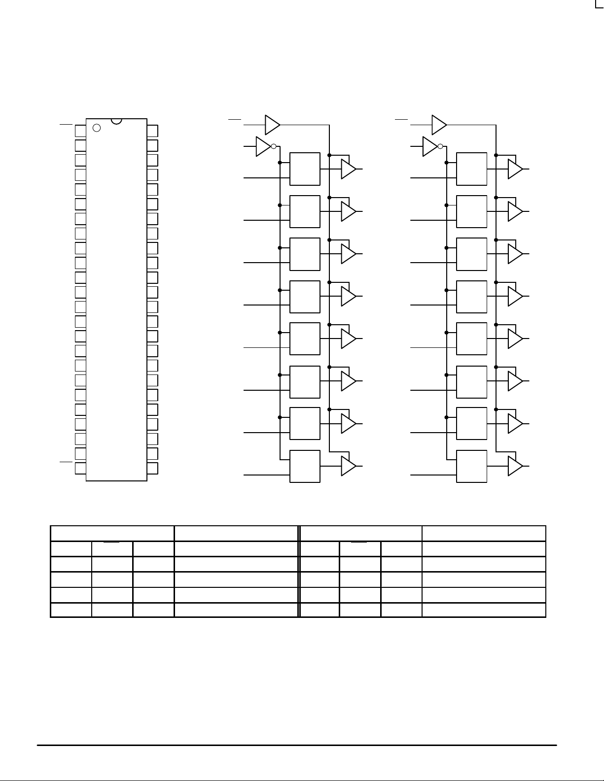
The MC74LCX16374 consists of 16 edge–triggered flip–flops with
individual D–type inputs and 5V–tolerant 3–state true outputs. The
buffered clocks (CPn) and buffered Output Enables (OEn
all flip–flops within the respective byte. The flip–flops will store the state of
individual D inputs that meet the setup and hold time requirements on the
LOW–to–HIGH Clock (CP) transition. With the OE
the flip–flops are available at the outputs. When the OE
outputs go to the high impedance state. The OE
the operation of the flip–flops.
input level does not affect
) are common to
LOW, the contents of
is HIGH, the
LOW–VOLTAGE
CMOS 16–BIT
D–TYPE FLIP–FLOP
• Designed for 2.7 to 3.6V V
• 6.2ns Maximum t
pd
Operation
CC
• 5V Tolerant — Interface Capability With 5V TTL Logic
• Supports Live Insertion and Withdrawal
• I
Specification Guarantees High Impedance When VCC = 0V
OFF
• LVTTL Compatible
• LVCMOS Compatible
• 24mA Balanced Output Sink and Source Capability
• Near Zero Static Supply Current in All Three Logic States (20µA)
Substantially Reduces System Power Requirements
• Latchup Performance Exceeds 500mA
• ESD Performance: Human Body Model >2000V; Machine Model >200V
PLASTIC TSSOP PACKAGE
PIN NAMES
Pins
OEn
CPn
D0–D15
O0–O15
DT SUFFIX
CASE 1201–01
Function
Output Enable Inputs
Clock Pulse Inputs
Inputs
Outputs
11/96
Motorola, Inc. 1996
1
REV 1
MC74LCX16374
LOGIC DIAGRAM
O3
V
CC
V
CC
O12
1
CP1OE1
481
D0O0
472
D1O1
463
GNDGND
454
D2O2
445
D3
436
V
427
CC
D4O4
418
D5O5
409
GNDGND
3910
D6O6
3811
D7O7
3712
D8O8
3613
D9O9
3514
GNDGND
3415
D10O10
3316
D11O11
3217
V
3118
CC
D12
3019
D13O13
2920
GNDGND
2821
D14O14
2722
D15O15
2623
CP2OE2
2524
OE1
CP1
D0
D1
D2
D3
D4
D5
D6
D7
48
47
46
44
43
41
40
38
37
nCP
D
nCP
D
nCP
D
nCP
D
nCP
D
nCP
D
nCP
D
nCP
D
2
3
5
6
8
9
11
12
O0
O1
O2
O3
O4
O5
O6
O7
Q
Q
Q
Q
Q
Q
Q
Q
OE2
CP2
D8
D9
D10
D11
D12
D13
D14
D15
24
25
36
35
33
32
30
29
27
26
nCP
D
nCP
D
nCP
D
nCP
D
nCP
D
nCP
D
nCP
D
nCP
D
13
14
16
17
19
20
22
23
O8
O9
O10
O11
O12
O13
O14
O15
Q
Q
Q
Q
Q
Q
Q
Q
Inputs Outputs Inputs Outputs
CP1 OE1 D0:7 O0:7 CP2 OE2 D8:15 O8:15
↑ L H H ↑ L H H
↑ L L L ↑ L L L
L L X O0 L L X O0
X H X Z X H X Z
H = High Voltage Level; L = Low Voltage Level; Z = High Impedance State; ↑ = Low–to–High Transition; X = High or Low Voltage Level and
Transitions Are Acceptable, for ICC reasons, DO NOT FLOAT Inputs
MOTOROLA LCX DATA
2
BR1339 — REV 3
 Loading...