

MOTOROLA MC74HCT573AN, MC74HCT573ADW, MC74HCT573ADT, MC74HCT573ADTR2, MC74HCT573AF Datasheet
...
Semiconductor Components Industries, LLC, 2000
March, 2000 – Rev. 8
1 Publication Order Number:
MC74HCT573A/D
MC74HCT573A
Octal 3-State Noninverting
Transparent Latch with
LSTTL Compatible Inputs
High–Performance Silicon–Gate CMOS
The MC74HCT573A is identical in pinout to the LS573. This
device may be used as a level converter for interfacing TTL or NMOS
outputs to High–Speed CMOS inputs.
These latches appear transparent to data (i.e., the outputs change
asynchronously) when Latch Enable is high. When Latch Enable goes
low, data meeting the setup and hold times becomes latched.
The Output Enable input does not affect the state of the latches, but
when Output Enable is high, all device outputs are forced to the
high–impedance state. Thus, data may be latched even when the
outputs are not enabled.
The HCT573A is identical in function to the HCT373A but has the
Data Inputs on the opposite side of the package from the outputs to
facilitate PC board layout.
• Output Drive Capability: 15 LSTTL Loads
• TTL/NMOS–Compatible Input Levels
• Outputs Directly Interface to CMOS, NMOS and TTL
• Operating Voltage Range: 4.5 to 5.5 V
• Low Input Current: 10 µA
• In Compliance with the Requirements Defined by JEDEC Standard
No. 7A
• Chip Complexity: 234 FETs or 58.5 Equivalent Gates
— Improved Propagation Delays
— 50% Lower Quiescent Power
http://onsemi.com
MARKING
DIAGRAMS
1
20
A = Assembly Location
WL = Wafer Lot
YY = Year
WW = Work Week
SOIC WIDE–20
DW SUFFIX
CASE 751D
HCT573A
AWLYYWW
PDIP–20
N SUFFIX
CASE 738
1
20
MC74HCT573AN
AWLYYWW
TSSOP–20
DT SUFFIX
CASE 948G
1
20
1
20
1
20
Device Package Shipping
ORDERING INFORMATION
MC74HCT573AN PDIP–20 1440 / Box
MC74HCT573ADW SOIC–WIDE
38 / Rail
MC74HCT573ADWR2 SOIC–WIDE 1000 / Reel
MC74HCT573ADT TSSOP–20 75 / Rail
MC74HCT573ADTR2 TSSOP–20
2500 / Reel
HCT
573A
ALYW
1
20
MC74HCT573A
http://onsemi.com
2
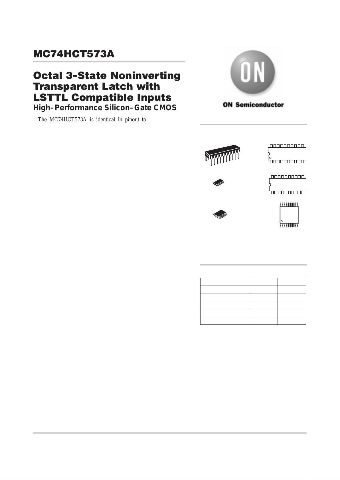
LOGIC DIAGRAM
DATA
INPUTS
D0
D1
D2
D3
D4
D5
D6
D7
LATCH ENABLE
OUTPUT ENABLE
11
1
9
8
7
6
5
4
3
219
18
17
16
15
14
13
12
Q0
Q1
Q2
Q3
Q4
Q5
Q6
Q7
PIN 20 = V
CC
PIN 10 = GND
NONINVERTING
OUTPUTS
PIN ASSIGNMENT
D4
D2
D1
D0
OUTPUT
ENABLE
GND
D7
D6
D5
D3 5
4
3
2
1
10
9
8
7
6
14
15
16
17
18
19
20
11
12
13
Q3
Q2
Q1
Q0
V
CC
LATCH
ENABLE
Q7
Q6
Q5
Q4
FUNCTION TABLE
Inputs Output
Output Latch
Enable Enable D Q
LHHH
LHLL
L L X No Change
HXXZ
X = Don’t Care
Z = High Impedance
Design Criteria
Value
Units
ОООООООО
Î
Internal Gate Count*
ÎÎ
Î
58.5
Î
Î
ea
Internal Gate Propagation Delay
1.5
ns
Internal Gate Power Dissipation
5.0
µW
Speed Power Product
0.0075
pJ
*Equivalent to a two–input NAND gate.
MC74HCT573A
http://onsemi.com
3
MAXIMUM RATINGS*
Symbol
Parameter
Value
Unit
V
CC
DC Supply Voltage (Referenced to GND)
– 0.5 to + 7.0
V
V
in
DC Input Voltage (Referenced to GND)
– 0.5 to VCC + 0.5
V
V
out
DC Output Voltage (Referenced to GND)
– 0.5 to VCC + 0.5
V
I
in
DC Input Current, per Pin
± 20
mA
I
out
DC Output Current, per Pin
± 25
mA
I
CC
DC Supply Current, VCC and GND Pins
± 50
mA
ÎÎ
Î
P
D
ОООООООООООО
Î
Power Dissipation in Still Air Plastic DIP†
SOIC Package†
TSSOP Package†
ÎÎÎ
Î
750
500
450
Î
Î
mW
T
stg
Storage Temperature
– 65 to + 150
_
C
ÎÎ
Î
T
L
ОООООООООООО
Î
Lead Temperature, 1 mm from Case for 10 Seconds
(Plastic DIP, TSSOP or SOIC Package)
ÎÎÎ
Î
260
Î
Î
_
C
*Maximum Ratings are those values beyond which damage to the device may occur.
Functional operation should be restricted to the Recommended Operating Conditions.
†Derating — Plastic DIP: –10 mW/_C from 65_ to 125_C
SOIC Package: –7 mW/_C from 65_ to 125_C
TSSOP Package: –6.1 mW/°C from 65_ to 125_C
For high frequency or heavy load considerations, see Chapter 2 of the ON Semiconductor High–Speed CMOS Data Book (DL129/D).
RECOMMENDED OPERATING CONDITIONS
Symbol
Parameter
Min
ÎÎ
Max
Unit
V
CC
DC Supply Voltage (Referenced to GND)
4.5
ÎÎ
5.5
V
Vin, V
out
DC Input Voltage, Output Voltage (Referenced to GND)
0
ÎÎ
V
CC
V
T
A
Operating Temperature, All Package Types
– 55
ÎÎ
+ 125
_
C
tr, t
f
Input Rise and Fall Time (Figure 1)
0
ÎÎ
500
ns
DC ELECTRICAL CHARACTERISTICS (Voltages Referenced to GND)
Guaranteed Limit
ÎÎ
Î
Symbol
ОООООООО
Î
Parameter
ООООООО
Î
Test Conditions
ÎÎ
Î
V
CC
V
Î
Î
– 55 to
25_C
ÎÎ
Î
v
85_C
ÎÎ
Î
v
125_C
Î
Î
Unit
V
IH
Minimum High–Level Input
Voltage
V
out
= 0.1 V or VCC – 0.1 V
|I
out
| v 20 µA
4.5
5.5
2.0
2.0
2.0
2.0
2.0
2.0
V
ÎÎ
Î
V
IL
ОООООООО
Î
Maximum Low–Level Input
Voltage
ООООООО
Î
V
out
= 0.1 V or VCC – 0.1 V
|I
out
| v 20 µA
ÎÎ
Î
4.5
5.5
Î
Î
0.8
0.8
ÎÎ
Î
0.8
0.8
ÎÎ
Î
0.8
0.8
Î
Î
V
V
OH
Minimum High–Level Output
Voltage
Vin = VIH or V
IL
|I
out
| v 20 µA
4.5
5.5
4.4
5.4
4.4
5.4
4.4
5.4
V
ÎÎÎООООООООÎООООООО
Î
Vin = VIH or V
IL
|I
out
| v 6.0 mA
ÎÎ
Î
4.5
Î
Î
3.98
ÎÎ
Î
3.84
ÎÎ
Î
3.7
Î
Î
V
OL
Maximum Low–Level Output
Voltage
Vin = VIH or V
IL
|I
out
| v 20 µA
4.5
5.5
0.1
0.1
0.1
0.1
0.1
0.1
V
ÎÎÎООООООООÎООООООО
Î
Vin = VIH or V
IL
|I
out
| v 6.0 mA
ÎÎ
Î
4.5
Î
Î
0.26
ÎÎ
Î
0.33
ÎÎ
Î
0.4
Î
Î
I
in
Maximum Input Leakage Current
Vin = VCC or GND
5.5
± 0.1
± 1.0
± 1.0
µA
ÎÎ
Î
I
OZ
ОООООООО
Î
Maximum Three–State
Leakage Current
ООООООО
Î
Output in High–Impedance State
Vin = VIL or V
IH
V
out
= VCC or GND
ÎÎ
Î
5.5
Î
Î
± 0.5
ÎÎ
Î
± 5.0
ÎÎ
Î
± 10
Î
Î
µA
ÎÎ
Î
I
CC
ОООООООО
Î
Maximum Quiescent Supply
Current (per Package)
ООООООО
Î
Vin = VCC or GND
I
out
v 0 µA
ÎÎ
Î
5.5
Î
Î
4.0
ÎÎ
Î
40
ÎÎ
Î
160
Î
Î
µA
∆I
CC
Additional Quiescent Supply
Vin = 2.4 V , Any One Input
p
≥ – 55_C
25_C to 125_C
Current
V
i
n
=
V
CC
or
GND, Other In uts
l
out
= 0 µA
5.5
2.9
2.4
mA
NOTE: Information on typical parametric values can be found in Chapter 2 of the ON Semiconductor High–Speed CMOS Data Book
(DL129/D).
This device contains protection
circuitry to guard against damage
due to high static voltages or electric
fields. However, precautions must
be taken to avoid applications of any
voltage higher than maximum rated
voltages to this high–impedance circuit. For proper operation, Vin and
V
out
should be constrained to the
range GND v (Vin or V
out
) v VCC.
Unused inputs must always be
tied to an appropriate logic voltage
level (e.g., either GND or VCC).
Unused outputs must be left open.
 Loading...