

MOTOROLA MC74HCT04ADT, MC74HCT04ADTR2, MC74HCT04ADR2, MC74HCT04AN, MC74HCT04AFL1 Datasheet
...
Semiconductor Components Industries, LLC, 2000
March, 2000 – Rev. 7
1 Publication Order Number:
MC74HCT04A/D
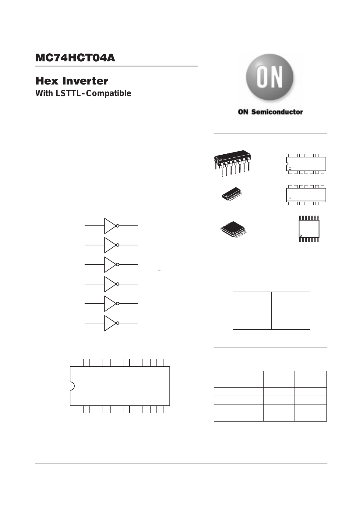
MC74HCT04A
Hex Inverter
With LSTTL–Compatible Inputs
High–Performance Silicon–Gate CMOS
The MC74HCT04A may be used as a level converter for interfacing
TTL or NMOS outputs to High–Speed CMOS inputs.
The HCT04A is identical in pinout to the LS04.
• Output Drive Capability: 10 LSTTL Loads
• TTL/NMOS–Compatible Input Levels
• Outputs Directly Interface to CMOS, NMOS and TTL
• Operating Voltage Range: 4.5 to 5.5V
• Low Input Current: 1µA
• In Compliance With the JEDEC Standard No. 7A Requirements
• Chip Complexity: 48 FETs or 12 Equivalent Gates
LOGIC DIAGRAM
Y1A1
A2
A3
A4
A5
A6
Y2
Y3
Y4
Y5
Y6
1
3
5
9
11
13
2
4
6
8
10
12
Y = A
Pin 14 = V
CC
Pin 7 = GND
Pinout: 14–Lead Packages (Top View)
1314 12 11 10 9 8
21 34567
V
CC
A6 Y6 A5 Y5 A4 Y4
A1 Y1 A2 Y2 A3 Y3 GND
Device Package Shipping
ORDERING INFORMATION
MC74HCT04AN PDIP–14 2000 / Box
MC74HCT04AD SOIC–14
http://onsemi.com
55 / Rail
MC74HCT04ADR2 SOIC–14 2500 / Reel
MARKING
DIAGRAMS
A = Assembly Location
WL or L = Wafer Lot
YY or Y = Year
WW or W = Work Week
MC74HCT04ADT TSSOP–14 96 / Rail
MC74HCT04ADTR2 TSSOP–14
2500 / Reel
TSSOP–14
DT SUFFIX
CASE 948G
HCT
04A
ALYW
1
14
1
14
PDIP–14
N SUFFIX
CASE 646
MC74HCT04AN
AWLYYWW
SOIC–14
D SUFFIX
CASE 751A
1
14
HCT04A
AWLYWW
L
H
FUNCTION TABLE
Inputs Outputs
A
H
L
Y
MC74HCT04A
http://onsemi.com
2
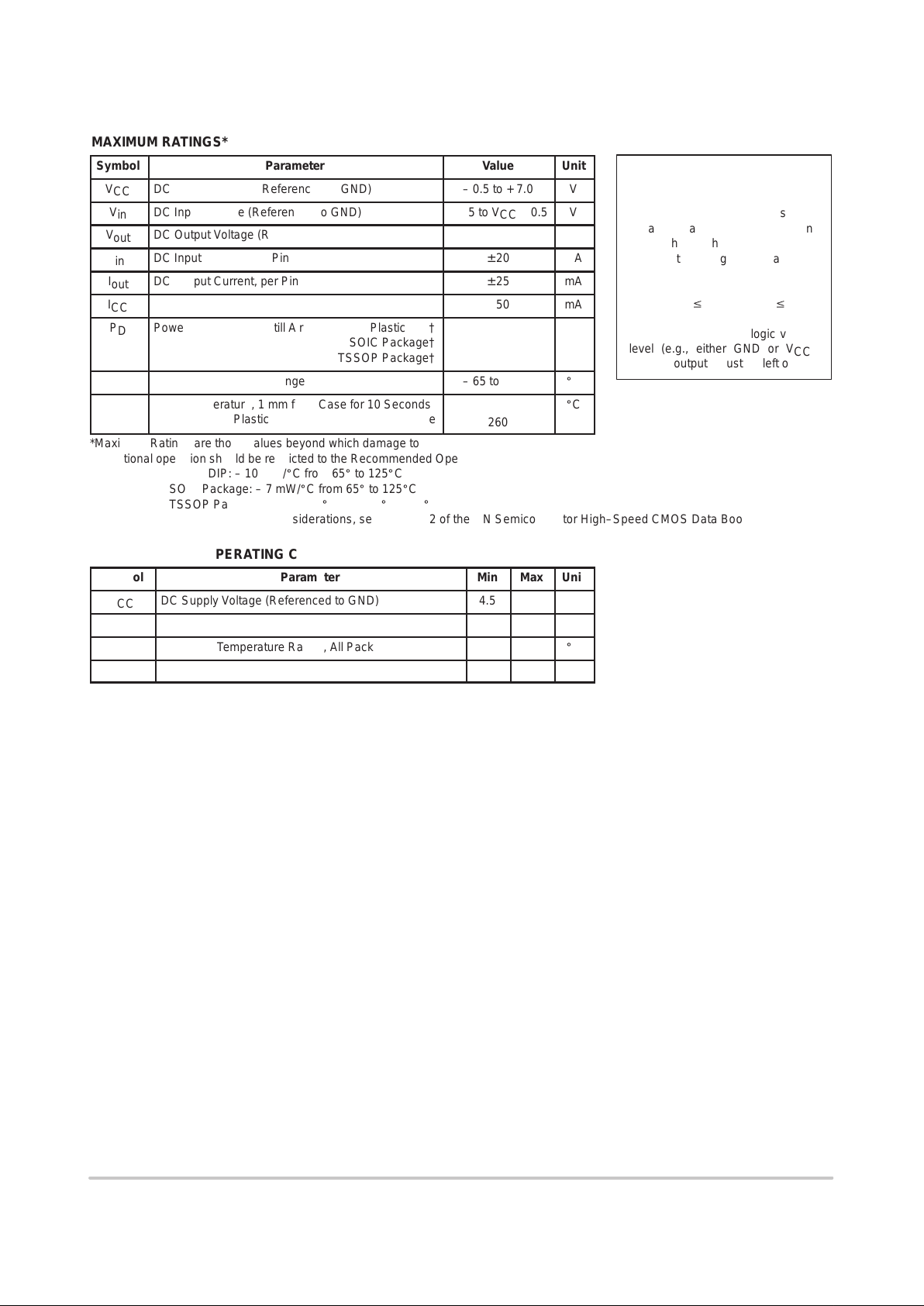
MAXIMUM RATINGS*
Symbol
Parameter
Value
Unit
V
CC
DC Supply Voltage (Referenced to GND)
– 0.5 to + 7.0
V
V
in
DC Input Voltage (Referenced to GND)
– 0.5 to VCC + 0.5
V
V
out
DC Output Voltage (Referenced to GND)
– 0.5 to VCC + 0.5
V
I
in
DC Input Current, per Pin
± 20
mA
I
out
DC Output Current, per Pin
± 25
mA
I
CC
DC Supply Current, VCC and GND Pins
± 50
mA
ÎÎ
Î
P
D
ОООООООООООО
Î
Power Dissipation in Still Air Plastic DIP†
SOIC Package†
TSSOP Package†
ÎÎÎ
Î
750
500
450
Î
Î
mW
T
stg
Storage Temperature Range
– 65 to + 150
_
C
ÎÎ
Î
T
L
ОООООООООООО
Î
Lead Temperature, 1 mm from Case for 10 Seconds
Plastic DIP, SOIC or TSSOP Package
ÎÎÎ
Î
260
Î
Î
_
C
*Maximum Ratings are those values beyond which damage to the device may occur.
Functional operation should be restricted to the Recommended Operating Conditions.
†Derating — Plastic DIP: – 10 mW/_C from 65_ to 125_C
SOIC Package: – 7 mW/_C from 65_ to 125_C
TSSOP Package: – 6.1 mW/_C from 65_ to 125_C
For high frequency or heavy load considerations, see Chapter 2 of the ON Semiconductor High–Speed CMOS Data Book (DL129/D).
RECOMMENDED OPERATING CONDITIONS
Symbol
Parameter
Min
ÎÎ
Max
Unit
V
CC
DC Supply Voltage (Referenced to GND)
4.5
ÎÎ
5.5
V
Vin, V
out
DC Input Voltage, Output Voltage (Referenced to GND)
0
ÎÎ
V
CC
V
T
A
Operating Temperature Range, All Package Types
– 55
ÎÎ
+ 125
_
C
tr, t
f
Input Rise/Fall Time (Figure 1)
0
ÎÎ
500
ns
This device contains protection
circuitry to guard against damage
due to high static voltages or electric
fields. However, precautions must
be taken to avoid applications of any
voltage higher than maximum rated
voltages to this high–impedance circuit. For proper operation, Vin and
V
out
should be constrained to the
range GND v (Vin or V
out
) v VCC.
Unused inputs must always be
tied to an appropriate logic voltage
level (e.g., either GND or VCC).
Unused outputs must be left open.
MC74HCT04A
http://onsemi.com
3
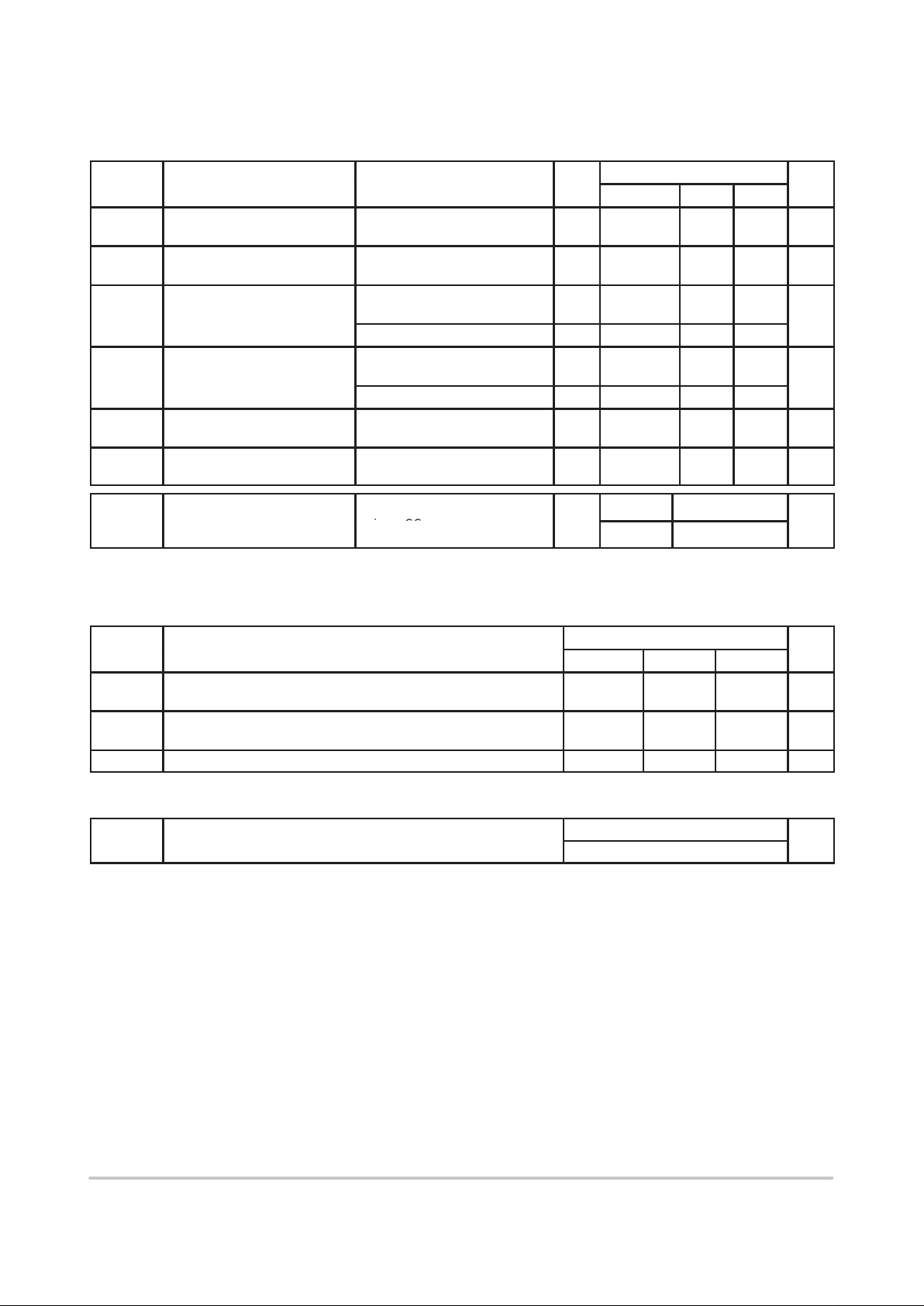
DC CHARACTERISTICS (Voltages Referenced to GND)
Guaranteed Limit
Symbol Parameter Condition
V
CC
V
–55 to 25°C ≤85°C ≤125°C Unit
V
IH
Minimum High–Level Input
Voltage
V
out
= 0.1V
|I
out
| ≤ 20µA
4.5
5.5
2.0
2.0
2.0
2.0
2.0
2.0
V
V
IL
Maximum Low–Level Input
Voltage
V
out
= VCC – 0.1V
|I
out
| ≤ 20µA
4.5
5.5
0.8
0.8
0.8
0.8
0.8
0.8
V
V
OH
Minimum High–Level Output
Voltage
Vin = V
IL
|I
out
| ≤ 20µA
4.5
5.5
4.4
5.4
4.4
5.4
4.4
5.4
V
Vin = V
IL
|I
out
| ≤ 4.0mA 4.5 3.98 3.84 3.70
V
OL
Maximum Low–Level Output
Voltage
Vin = V
IH
|I
out
| ≤ 20µA
4.5
5.5
0.1
0.1
0.1
0.1
0.1
0.1
V
Vin = V
IH
|I
out
| ≤ 4.0mA 4.5 0.26 0.33 0.40
I
in
Maximum Input Leakage
Current
Vin = VCC or GND 5.5 ±0.1 ±1.0 ±1.0 µA
I
CC
Maximum Quiescent Supply
Current (per Package)
Vin = VCC or GND
I
out
= 0µA
5.5 1 10 40 µA
∆I
CC
Additional Quiescent Supply
Vin = 2.4V , Any One Input
p
≥ –55°C 25 to 125°C
C
urren
t
V
in
=
V
CC
or
GND, Oth
er Inputs
I
out
= 0µA
5.5
2.9 2.4
mA
1. Information on typical parametric values can be found in Chapter 2 of the ON Semiconductor High–Speed CMOS Data Book (DL129/D).
2. Total Supply Current = ICC + Σ∆ICC.
AC CHARACTERISTICS (V
CC
= 5.0V ±10%, CL = 50pF, Input tr = tf = 6ns)
Guaranteed Limit
Symbol Parameter –55 to 25°C ≤85°C ≤125°C Unit
t
PLH
,
t
PHL
Maximum Propagation Delay, Input A to Output Y
(Figures 1 and 2)
15
17
19
21
22
26
ns
t
TLH
,
t
THL
Maximum Output Transition Time, Any Output
(Figures 1 and 2)
15 19 22 ns
C
in
Maximum Input Capacitance 10 10 10 pF
NOTE: For propagation delays with loads other than 50 pF, and information on typical parametric values, see Chapter 2 of the ON
Semiconductor High–Speed CMOS Data Book (DL129/D).
Typical @ 25°C, VCC = 5.0 V
C
PD
Power Dissipation Capacitance (Per Inverter)*
22
pF
*Used to determine the no–load dynamic power consumption: PD = CPD V
CC
2
f + ICC VCC. For load considerations, see Chapter 2 of the
ON Semiconductor High–Speed CMOS Data Book (DL129/D).
 Loading...