

Motorola MC74HC85DT, MC74HC85N Datasheet

SEMICONDUCTOR TECHNICAL DATA
1
REV 6
Motorola, Inc. 1995
10/95
High–Performance Silicon–Gate CMOS
The MC74HC85 is identical in pinout and function to the LS85. This device
is similar in function to the MM74C85 and L85, but has a different pinout. The
device inputs are compatible with standard CMOS outputs; with pullup
resistors, they are compatible with LSTTL outputs.
This 4–Bit Magnitude Comparator compares two 4–bit nibbles and gives a
high voltage level on either the A > B
out
, A = B
out
, or A < B
out
output, leaving
the other two at a low voltage level. This device also has A > Bin, A = Bin, and
A < Bin inputs, eliminating the need for external gates when cascading.
• Output Drive Capability: 10 LSTTL Loads
• Outputs Directly Interface to CMOS, NMOS, and TTL
• Operating Voltage Range: 2 to 6 V
• Low Input Current: 1 µA
• High Noise Immunity Characteristic of CMOS Devices
• In Compliance with the Requirements Defined by JEDEC Standard
No. 7A
• Chip Complexity: 248 FETs or 62 Equivalent Gates
LOGIC DIAGRAM
5
6
7
10
A > B
out
A = B
out
A < B
out
A0
PIN 16 = V
CC
PIN 8 = GND
COMPARISON
OUTPUTS
DATA
INPUTS
CASCADING
INPUTS
12
13
15
9
11
14
1
4
3
2
A1
A2
A3
B0
B1
B2
B3
A > B
in
A = B
in
A < B
in
PIN ASSIGNMENT
13
14
15
16
9
10
11
125
4
3
2
1
8
7
6
A1
A2
B2
A3
V
CC
B0
A0
B1
A
t
B
in
B3
A = B
in
A
u
B
in
A u B
out
A = B
out
A
t
B
out
GND
N SUFFIX
PLASTIC PACKAGE
CASE 648–08
ORDERING INFORMATION
MC74HCXXN
MC74HCXXDT
Plastic
TSSOP
1
16
1
16
DT SUFFIX
TSSOP PACKAGE
CASE 948F–01
MC74HC85
MOTOROLA High–Speed CMOS Logic Data
DL129 — Rev 6
2
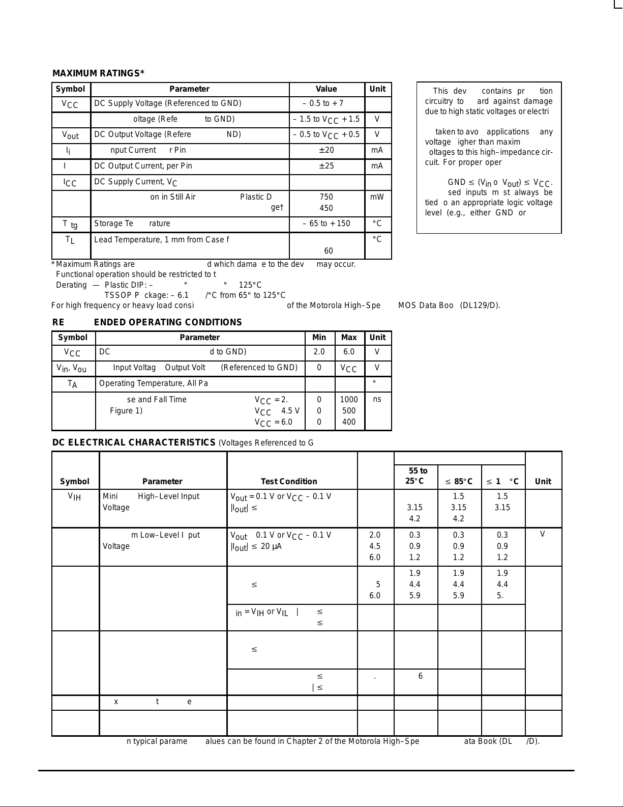
MAXIMUM RATINGS*
Symbol
Parameter
Value
Unit
V
CC
DC Supply Voltage (Referenced to GND)
– 0.5 to + 7.0
V
V
in
DC Input Voltage (Referenced to GND)
– 1.5 to VCC + 1.5
V
V
out
DC Output Voltage (Referenced to GND)
– 0.5 to VCC + 0.5
V
I
in
DC Input Current, per Pin
± 20
mA
I
out
DC Output Current, per Pin
± 25
mA
I
CC
DC Supply Current, VCC and GND Pins
± 50
mA
P
D
Power Dissipation in Still Air Plastic DIP†
TSSOP Package†
750
450
mW
T
stg
Storage Temperature
– 65 to + 150
_
C
T
L
Lead Temperature, 1 mm from Case for 10 Seconds
(Plastic DIP or TSSOP)
260
_
C
*Maximum Ratings are those values beyond which damage to the device may occur.
Functional operation should be restricted to the Recommended Operating Conditions.
†Derating — Plastic DIP: – 10 mW/_C from 65_ to 125_C
TSSOP Package: – 6.1 mW/_C from 65_ to 125_C
For high frequency or heavy load considerations, see Chapter 2 of the Motorola High–Speed CMOS Data Book (DL129/D).
RECOMMENDED OPERATING CONDITIONS
Symbol
Parameter
Min
Max
Unit
V
CC
DC Supply Voltage (Referenced to GND)
2.0
6.0
V
Vin, V
out
DC Input Voltage, Output Voltage (Referenced to GND)
0
V
CC
V
T
A
Operating Temperature, All Package Types
– 55
+ 125
_
C
tr, t
f
Input Rise and Fall Time VCC = 2.0 V
(Figure 1) VCC = 4.5 V
VCC = 6.0 V
0
0
0
1000
500
400
ns
DC ELECTRICAL CHARACTERISTICS (Voltages Referenced to GND)
Guaranteed Limit
Symbol
Parameter
Test Conditions
V
CC
V
– 55 to
25_C
v
85_Cv 125_C
Unit
V
IH
Minimum High–Level Input
Voltage
V
out
= 0.1 V or VCC – 0.1 V
|I
out
| v 20 µA
2.0
4.5
6.0
1.5
3.15
4.2
1.5
3.15
4.2
1.5
3.15
4.2
V
V
IL
Maximum Low–Level Input
Voltage
V
out
= 0.1 V or VCC – 0.1 V
|I
out
| v 20 µA
2.0
4.5
6.0
0.3
0.9
1.2
0.3
0.9
1.2
0.3
0.9
1.2
V
Vin = VIH or V
IL
|I
out
| v 20 µA
2.0
4.5
6.0
1.9
4.4
5.9
1.9
4.4
5.9
1.9
4.4
5.9
Vin = VIH or VIL|I
out
| v 4.0 mA
|I
out
| v 5.2 mA
4.5
6.0
3.98
5.48
3.84
5.34
3.70
5.20
Vin = VIH or V
IL
|I
out
| v 20 µA
2.0
4.5
6.0
0.1
0.1
0.1
0.1
0.1
0.1
0.1
0.1
0.1
Vin = VIH or VIL|I
out
| v 4.0 mA
|I
out
| v 5.2 mA
4.5
6.0
0.26
0.26
0.33
0.33
0.40
0.40
I
in
Maximum Input Leakage Current
Vin = VCC or GND
6.0
± 0.1
± 1.0
± 1.0
µA
I
CC
Maximum Quiescent Supply
Current (per Package)
Vin = VCC or GND
I
out
= 0 µA
6.0
8
80
160
µA
NOTE: Information on typical parametric values can be found in Chapter 2 of the Motorola High–Speed CMOS Data Book (DL129/D).
This device contains protection
circuitry to guard against damage
due to high static voltages or electric
fields. However, precautions must
be taken to avoid applications of any
voltage higher than maximum rated
voltages to this high–impedance circuit. For proper operation, Vin and
V
out
should be constrained to the
range GND v (Vin or V
out
) v VCC.
Unused inputs must always be
tied to an appropriate logic voltage
level (e.g., either GND or VCC).
Unused outputs must be left open.
V
OH
V
OL
Minimum High–Level Output
Voltage
Maximum Low–Level Output
Voltage
V
V

MC74HC85
High–Speed CMOS Logic Data
DL129 — Rev 6
3 MOTOROLA
AC ELECTRICAL CHARACTERISTICS (C
L
= 50 pF, Input tr = tf = 6 ns)
Guaranteed Limit
Symbol
Parameter
V
CC
V
– 55 to
25_C
v
85_Cv 125_C
Unit
t
PLH
,
t
PHL
Maximum Propagation Delay, Inputs A or B to Outputs A> B
or A < B
(Figures 1 and 2)
2.0
4.5
6.0
230
46
39
290
58
49
345
69
59
ns
t
PLH
,
t
PHL
Maximum Propagation Delay, Inputs A or B to Output A = B
(Figures 1 and 2)
2.0
4.5
6.0
200
40
34
250
50
43
300
60
51
ns
t
PLH
,
t
PHL
Maximum Propagation Delay, Inputs A < B or A = B to Output A > B
(Figures 1 and 2)
2.0
4.5
6.0
175
35
30
220
44
37
265
53
45
ns
t
PLH
,
t
PHL
Maximum Propagation Delay, Inputs A>B or A = B to Output A < B
(Figures 1 and 2)
2.0
4.5
6.0
175
35
30
220
44
37
265
53
45
ns
t
PLH
,
t
PHL
Maximum Propagation Delay, Input A = B to Output A = B
(Figures 1 and 2)
2.0
4.5
6.0
145
29
25
180
36
31
220
44
38
ns
t
TLH
,
t
THL
Maximum Output Transition Time, Any Output
(Figures 1 and 2)
2.0
4.5
6.0
75
15
13
95
19
16
110
22
19
ns
C
in
Maximum Input Capacitance
—
10
10
10
pF
NOTES:
1. For propagation delays with loads other than 50 pF, see Chapter 2 of the Motorola High–Speed CMOS Data Book (DL129/D).
2. Information on typical parametric values can be found in Chapter 2 of the Motorola High–Speed CMOS Data Book (DL129/D).
Typical @ 25°C, VCC = 5.0 V
50
*Used to determine the no–load dynamic power consumption: PD = CPD V
CC
2
f + ICC VCC. For load considerations, see Chapter 2 of the
Motorola High–Speed CMOS Data Book (DL129/D).
Figure 1. Switching Waveforms
10%
10%
90%
50%
90%
50%
50%
t
r
t
f
INPUTS
OUTPUTS
t
PLH
t
PHL
t
PLH
t
PHL
t
THL
t
TLH
OUTPUTS
V
CC
GND
*Includes all probe and jig capacitance
CL*
TEST POINT
DEVICE
UNDER
TEST
OUTPUT
Figure 2. Test Circuit
C
PD
Power Dissipation Capacitance (Per Package)*
pF
 Loading...