

MOTOROLA MC74HC4852AFL2, MC74HC4852AFR1, MC74HC4852AFR2, MC74HC4852AN, MC74HC4852AFEL Datasheet
...
Semiconductor Components Industries, LLC, 2000
March, 2000 – Rev. 4
1 Publication Order Number:
MC74HC4851A/D
MC74HC4851A,
MC74HC4852A
Analog Multiplexers/
Demultiplexers with
Injection Current Effect
Control
Automotive Customized
These devices are pin compatible to standard HC405x and
MC1405xB analog mux/demux devices, but feature injection current
effect control. This makes them especially suited for usage in
automotive applications where voltages in excess of normal logic
voltage are common.
The injection current effect control allows signals at disabled analog
input channels to exceed the supply voltage range without affecting
the signal of the enabled analog channel. This eliminates the need for
external diode/ resistor networks typically used to keep the analog
channel signals within the supply voltage range.
The devices utilize low power silicon gate CMOS technology. The
Channel Select and Enable inputs are compatible with standard CMOS
outputs.
• Injection Current Cross–Coupling Less than 1mV/mA (See Figure 9)
• Pin Compatible to HC405X and MC1405XB Devices
• Power Supply Range (V
CC
– GND) = 2.0 to 6.0 V
• In Compliance With the Requirements of JEDEC Standard No. 7A
• Chip Complexity: 154 FETs or 36 Equivalent Gates
http://onsemi.com
MARKING
DIAGRAMS
1
16
PDIP–16
N SUFFIX
CASE 648
HC485xAN
AWLYYWW
SOIC–16
D SUFFIX
CASE 751B
TSSOP–16
DT SUFFIX
CASE 948F
1
16
HC485xAD
AWLYWW
HC48
5xA
ALYW
1
16
A = Assembly Location
WL or L = Wafer Lot
YY or Y = Year
WW or W = Work Week
SOIC–16 WIDE
DW SUFFIX
CASE 751G
1
16
HC485xADW
AWLYWW
See detailed ordering and shipping information in the package
dimensions section on page 10 of this data sheet.
ORDERING INFORMATION
MC74HC4851A, MC74HC4852A
http://onsemi.com
2
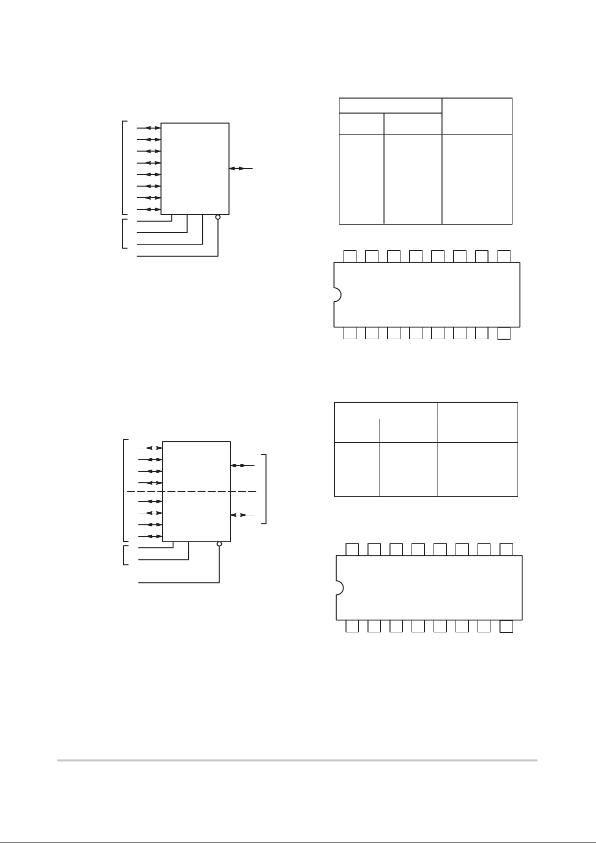
Figure 1. MC74HC4851A Logic Diagram
Single–Pole, 8–Position Plus Common Off
X0
13
X1
14
X2
15
X3
12
X4
1
X5
5
X6
2
X7
4
A
11
B
10
C
9
ENABLE
6
MULTIPLEXER/
DEMULTIPLEXER
X
3
ANALOG
INPUTS/
CHANNEL
INPUTS
PIN 16 = V
CC
PIN 8 = GND
COMMON
OUTPUT/
INPUT
1516 14 13 12 11 10
21 34567
V
CC
9
8
X2 X1 X0 X3 A B C
X4 X6 X X7 X5 Enable NC GND
Figure 2. MC74HC4851A 16–Lead Pinout (Top View)
OUTPUTS
SELECT
L
L
L
L
H
H
H
H
X
L
L
H
H
L
L
H
H
X
L
H
L
H
L
H
L
H
X
FUNCTION TABLE – MC74HC4851A
Control Inputs
ON Channels
Enable
Select
CBA
X0
X1
X2
X3
X4
X5
X6
X7
NONE
L
L
L
L
L
L
L
L
H
Figure 3. MC74HC4852A Logic Diagram
Double–Pole, 4–Position Plus Common Off
X0
12
X1
14
X2
15
X3
11
Y0
1
Y1
5
Y2
2
Y3
4
A
10
B
9
ENABLE
6
X SWITCH
Y SWITCH
X
13
ANALOG
INPUTS/OUTPUTS
CHANNEL-SELECT
INPUTS
PIN 16 = V
CC
PIN 8 = GND
COMMON
OUTPUTS/INPUTS
L
L
H
H
X
L
H
L
H
X
FUNCTION TABLE – MC74HC4852A
Control Inputs
ON Channels
Enable
Select
BA
X0
X1
X2
X3
L
L
L
L
H
X = Don’t Care
Figure 4. MC74HC4852A 16–Lead Pinout (Top View)
1516 14 13 12 11 10
21 34567
V
CC
9
8
X2 X1 X X0 X3 A B
Y0 Y2 Y Y3 Y1 Enable NC GND
Y
3
Y0
Y1
Y2
Y3
NONE
MC74HC4851A, MC74HC4852A
http://onsemi.com
3
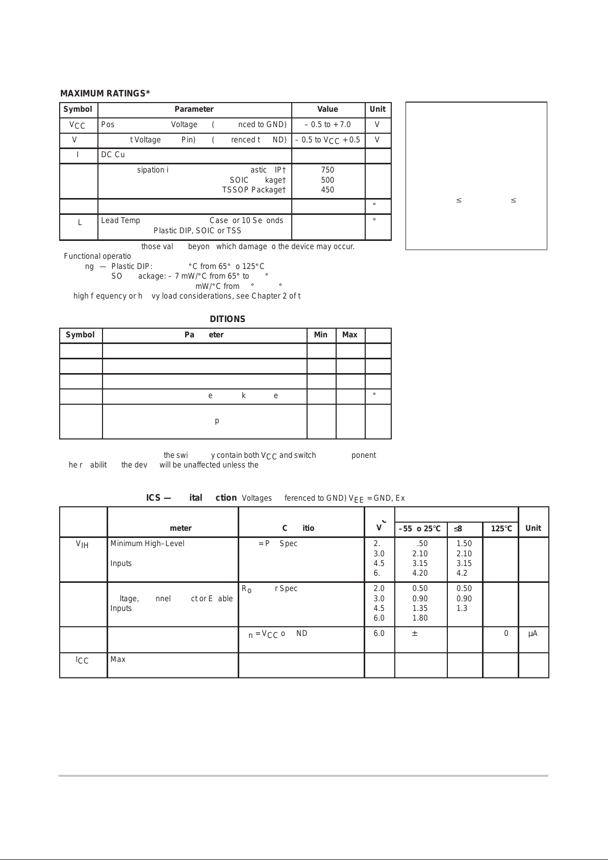
MAXIMUM RATINGS*
Symbol
Parameter
Value
Unit
V
CC
Positive DC Supply Voltage (Referenced to GND)
– 0.5 to + 7.0
V
V
in
DC Input Voltage (Any Pin) (Referenced to GND)
– 0.5 to VCC + 0.5
V
I
DC Current, Into or Out of Any Pin
± 25
mA
ÎÎ
Î
P
D
ОООООООООООО
Î
Power Dissipation in Still Air, Plastic DIP†
SOIC Package†
TSSOP Package†
ÎÎÎ
Î
750
500
450
Î
Î
mW
T
stg
Storage Temperature Range
– 65 to + 150
_
C
ÎÎ
Î
T
L
ОООООООООООО
Î
Lead Temperature, 1 mm from Case for 10 Seconds
Plastic DIP, SOIC or TSSOP Package
ÎÎÎ
Î
260
Î
Î
_
C
*Maximum Ratings are those values beyond which damage to the device may occur.
Functional operation should be restricted to the Recommended Operating Conditions.
†Derating — Plastic DIP: – 10 mW/_C from 65_ to 125_C
SOIC Package: – 7 mW/_C from 65_ to 125_C
TSSOP Package: – 6.1 mW/_C from 65_ to 125_C
For high frequency or heavy load considerations, see Chapter 2 of the ON Semiconductor High–Speed CMOS Data Book (DL129/D).
RECOMMENDED OPERATING CONDITIONS
Symbol
Parameter
Min
ÎÎ
Max
Unit
V
CC
Positive DC Supply Voltage (Referenced to GND)
2.0
ÎÎ
6.0
V
V
in
DC Input Voltage (Any Pin) (Referenced to GND)
GND
ÎÎ
V
CC
V
VIO*
Static or Dynamic Voltage Across Switch
0.0
ÎÎ
1.2
V
T
A
Operating Temperature Range, All Package T ypes
– 55
ÎÎ
+ 125
_
C
ÎÎ
Î
tr, t
f
ООООООООООООО
Î
Input Rise/Fall Time VCC = 2.0 V
(Channel Select or Enable Inputs) VCC = 4.5 V
VCC = 6.0 V
Î
Î
0
0
0
ÎÎ
ÎÎ
1000
500
400
Î
Î
ns
*For voltage drops across switch greater than 1.2V (switch on), excessive VCC current may be
drawn; i.e., the current out of the switch may contain both VCC and switch input components.
The reliability of the device will be unaffected unless the Maximum Ratings are exceeded.
DC CHARACTERISTICS — Digital Section (Voltages Referenced to GND) V
EE
= GND, Except Where Noted
V
Guaranteed Limit
Symbol Parameter Condition
V
CC
V
–55 to 25°C ≤85°C ≤125°C
Unit
V
IH
Minimum High–Level Input
Voltage, Channel–Select or Enable
Inputs
Ron = Per Spec 2.0
3.0
4.5
6.0
1.50
2.10
3.15
4.20
1.50
2.10
3.15
4.20
1.50
2.10
3.15
4.20
V
V
IL
Maximum Low–Level Input
Voltage, Channel–Select or Enable
Inputs
Ron = Per Spec 2.0
3.0
4.5
6.0
0.50
0.90
1.35
1.80
0.50
0.90
1.35
1.80
0.50
0.90
1.35
1.80
V
I
in
Maximum Input Leakage Current
on Digital Pins (Enable/A/B/C)
Vin = VCC or GND 6.0 ± 0.1 ± 1.0 ± 1.0 µA
I
CC
Maximum Quiescent Supply
Current (per Package)
V
in(digital)
= VCC or GND
V
in(analog)
= GND
6.0 2 20 40 µA
NOTE: Information on typical parametric values can be found in Chapter 2 of the ON Semiconductor High–Speed CMOS Data Book (DL129/D).
This device contains protection
circuitry to guard against damage
due to high static voltages or electric
fields. However, precautions must
be taken to avoid applications of any
voltage higher than maximum rated
voltages to this high–impedance circuit. For proper operation, Vin and
V
out
should be constrained to the
range GND v (Vin or V
out
) v VCC.
Unused inputs must always be
tied to an appropriate logic voltage
level (e.g., either GND or VCC).
Unused outputs must be left open.
MC74HC4851A, MC74HC4852A
http://onsemi.com
4
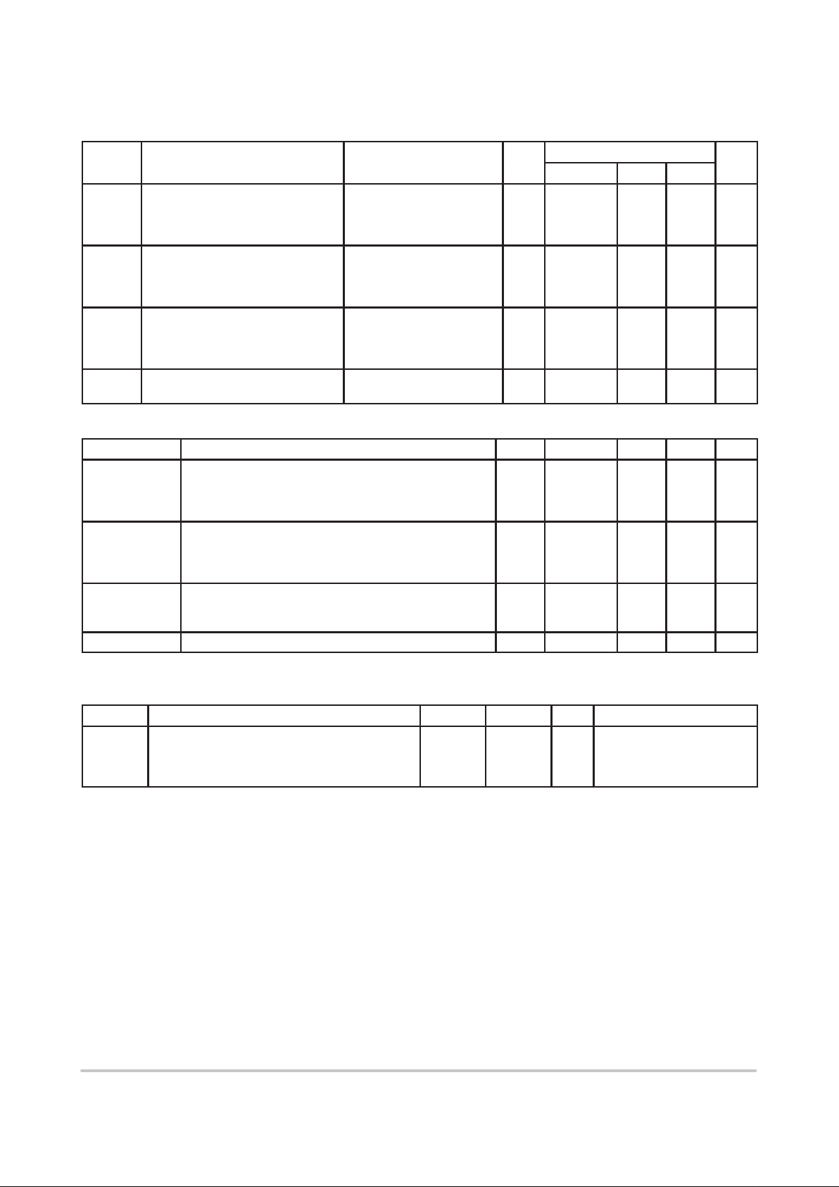
DC CHARACTERISTICS — Analog Section
Guaranteed Limit
Symbol Parameter Condition V
CC
–55 to 25°C ≤85°C ≤125°C
Unit
R
on
Maximum “ON” Resistance Vin = VIL or VIH;VIS = VCC to
GND; IS ≤ 2.0 mA
2.0
3.0
4.5
6.0
1700
1100
550
400
1750
1200
650
500
1800
1300
750
600
Ω
∆R
on
Delta “ON” Resistance Vin = VIL or VIH; VIS = VCC/2
IS ≤ 2.0 mA
2.0
3.0
4.5
6.0
300
160
80
60
400
200
100
80
500
240
120
100
Ω
I
off
Maximum Off–Channel Leakage
Current,
Any One Channel
Common Channel
Vin = VCC or GND
6.0 ±0.1
±0.2
±0.5
±2.0
±1.0
±4.0
µA
I
on
Maximum On–Channel Leakage
Channel–to–Channel
Vin = VCC or GND
6.0 ±0.2 ±2.0 ±4.0
µA
AC CHARACTERISTICS (C
L
= 50 pF, Input tr = tf = 6 ns)
Symbol Parameter V
CC
–55 to 25°C ≤85°C ≤125°C Unit
t
PHL
,
t
PLH
Maximum Propagation Delay , Analog Input to Analog Output 2.0
3.0
4.5
6.0
160
80
40
30
180
90
45
35
200
100
50
40
ns
t
PHL
, t
PHZ,PZH
t
PLH
, t
PLZ,PZL
Maximum Propagation Delay , Enable or Channel–Select to
Analog Output
2.0
3.0
4.5
6.0
260
160
80
60
280
180
90
70
300
200
100
80
ns
C
in
Maximum Input Capacitance Digital Pins
(All Switches Off) Any Single Analog Pin
(All Switches Off) Common Analog Pin
10
35
130
10
35
130
10
35
130
pF
C
PD
Power Dissipation Capacitance Typical 5.0 20 pF
INJECTION CURRENT COUPLING SPECIFICATIONS (V
CC
= 5V, TA = –55°C to +125°C)
Symbol Parameter Typ Max Unit Condition
V∆
out
Maximum Shift of Output Voltage of Enabled Analog
Channel
0.1
1.0
0.5
5.0
1.0
5.0
2.0
20
mV Iin* ≤ 1mA, RS ≤ 3,9kΩ
Iin* ≤ 10mA, RS ≤ 3,9kΩ
Iin* ≤ 1mA, RS ≤ 20kΩ
Iin* ≤ 10mA, RS ≤ 20kΩ
* Iin = T otal current injected into all disabled channels.
 Loading...