

MOTOROLA MC74HC4538AN, MC74HC4538DTEL, MC74HC4538AFR2, MC74HC4538AFEL, MC74HC4538AFL1 Datasheet
...
Semiconductor Components Industries, LLC, 2000
March, 2000 – Rev. 7
1 Publication Order Number:
MC74HC4538A/D
MC74HC4538A
Dual Precision
Monostable Multivibrator
(Retriggerable, Resettable)
The MC74HC4538A is identical in pinout to the MC14538B. The
device inputs are compatible with standard CMOS outputs; with
pullup resistors, they are compatible with LSTTL outputs.
This dual monostable multivibrator may be triggered by either the
positive or the negative edge of an input pulse, and produces a
precision output pulse over a wide range of pulse widths. Because the
device has conditioned trigger inputs, there are no trigger–input rise
and fall time restrictions. The output pulse width is determined by the
external timing components, Rx and Cx. The device has a reset
function which forces the Q output low and the Q
output high,
regardless of the state of the output pulse circuitry.
• Unlimited Rise and Fall Times Allowed on the Trigger Inputs
• Output Pulse is Independent of the Trigger Pulse Width
• ± 10% Guaranteed Pulse Width Variation from Part to Part (Using
the Same Test Jig)
• Output Drive Capability: 10 LSTTL Loads
• Outputs Directly Interface to CMOS, NMOS and TTL
• Operating Voltage Range: 3.0 to 6.0 V
• Low Input Current: 1.0 µA
• High Noise Immunity Characteristic of CMOS Devices
• In Compliance with the Requirements Defined by JEDEC Standard
No. 7A
• Chip Complexity: 145 FETs or 36 Equivalent Gates
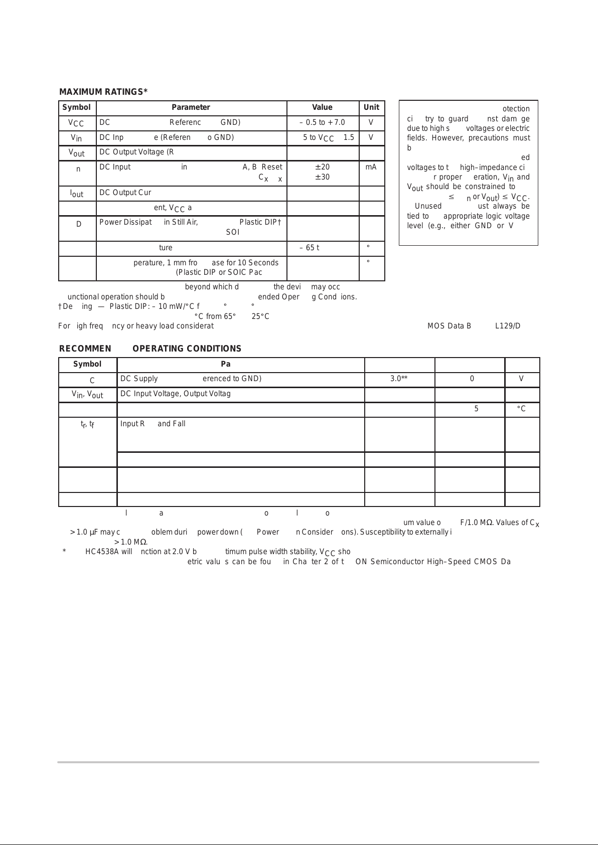
LOGIC DIAGRAM
PIN 16 = V
CC
PIN 8 = GND
RX AND CX ARE EXTERNAL COMPONENTS
PIN 1 AND PIN 15 MUST BE HARD WIRED TO GND
CX1R
X
1
V
CC
Q1
RESET 1
B1
A1
TRIGGER
INPUTS
Q1
12
4
5
3
6
7
CX2R
X
2
V
CC
Q2
RESET 2
B2
A2
TRIGGER
INPUTS
Q2
15 14
12
11
13
10
9
SO–16
D SUFFIX
CASE 751B
http://onsemi.com
1
16
PDIP–16
N SUFFIX
CASE 648
1
16
MARKING
DIAGRAMS
1
16
MC74HC4538AN
AWLYYWW
1
16
HC4538A
AWLYWW
A = Assembly Location
WL = Wafer Lot
YY = Year
WW = Work Week
Device Package Shipping
ORDERING INFORMATION
MC74HC4538AN PDIP–16 2000 / Box
MC74HC4538AD SOIC–16
48 / Rail
MC74HC4538ADR2 SOIC–16 2500 / Reel
PIN ASSIGNMENT
13
14
15
16
9
10
11
125
4
3
2
1
8
7
6
A2
RESET 2
CX2/RX2
GND
V
CC
Q2
Q2
B2
A1
RESET 1
CX1/RX1
GND
GND
Q1
Q1
B1
FUNCTION TABLE
Inputs Outputs
Reset A B Q Q
HH
HL
H X L Not Triggered
H H X Not Triggered
H L,H, H Not Triggered
H L L,H, Not Triggered
LX X LH
X X Not Triggered
MC74HC4538A
http://onsemi.com
2
MAXIMUM RATINGS*
Symbol
Parameter
Value
Unit
V
CC
DC Supply Voltage (Referenced to GND)
– 0.5 to + 7.0
V
V
in
DC Input Voltage (Referenced to GND)
– 1.5 to VCC + 1.5
V
V
out
DC Output Voltage (Referenced to GND)
– 0.5 to VCC + 0.5
ÎÎ
Î
I
in
ОООООООООООО
Î
DC Input Current, per Pin A, B, Reset
Cx, R
x
ÎÎÎ
Î
± 20
± 30
Î
Î
mA
I
out
DC Output Current, per Pin
± 25
mA
I
CC
DC Supply Current, VCC and GND Pins
± 50
mA
P
D
Power Dissipation in Still Air, Plastic DIP†
SOIC Package†
750
500
mW
T
stg
Storage Temperature
– 65 to + 150
_
C
ÎÎ
Î
T
L
ОООООООООООО
Î
Lead Temperature, 1 mm from Case for 10 Seconds
(Plastic DIP or SOIC Package)
ÎÎÎ
Î
260
Î
Î
_
C
*Maximum Ratings are those values beyond which damage to the device may occur.
Functional operation should be restricted to the Recommended Operating Conditions.
†Derating — Plastic DIP: – 10 mW/_C from 65_ to 125_C
SOIC Package: – 7 mW/_C from 65_ to 125_C
For high frequency or heavy load considerations, see Chapter 2 of the ON Semiconductor High–Speed CMOS Data Book (DL129/D).
RECOMMENDED OPERATING CONDITIONS
Symbol
Parameter
Min
Max
Unit
V
CC
DC Supply Voltage (Referenced to GND)
3.0**
6.0
V
Vin, V
out
DC Input Voltage, Output Voltage (Referenced to GND)
0
V
CC
V
T
A
Operating Temperature, All Package Types
– 55
+ 125
_
C
ÎÎÎ
Î
tr, t
f
ОООООООООООООООО
Î
Input Rise and Fall Time VCC = 2.0 V
(Figure 7) VCC = 4.5 V
VCC = 6.0 V
ÎÎÎ
Î
0
0
0
ÎÎÎÎ
Î
1000
500
400
Î
Î
ns
A or B (Figure 5)
—
No Limit
ÎÎÎ
Î
R
x
ОООООООООООООООО
Î
External Timing Resistor VCC < 4.5 V
VCC ≥ 4.5 V
ÎÎÎ
Î
1.0
2.0
ÎÎÎÎ
Î
*
*
Î
Î
kΩ
C
x
External Timing Capacitor
0
*
µF
*The maximum allowable values of Rx and Cx are a function of the leakage of capacitor Cx, the leakage of the HC4538A, and leakage due
to board layout and surface resistance. For most applications, Cx/Rx should be limited to a maximum value of 10 µF/1.0 MΩ. Values of C
x
> 1.0 µF may cause a problem during power down (see Power Down Considerations). Susceptibility to externally induced noise signals may
occur for Rx > 1.0 MΩ.
**The HC4538A will function at 2.0 V but for optimum pulse width stability, VCC should be above 3.0 V .
NOTE: Information on typical parametric values can be found in Chapter 2 of the ON Semiconductor High–Speed CMOS Data Book
(DL129/D).
This device contains protection
circuitry to guard against damage
due to high static voltages or electric
fields. However, precautions must
be taken to avoid applications of any
voltage higher than maximum rated
voltages to this high–impedance circuit. For proper operation, Vin and
V
out
should be constrained to the
range GND v (Vin or V
out
) v VCC.
Unused inputs must always be
tied to an appropriate logic voltage
level (e.g., either GND or VCC).
Unused outputs must be left open.
MC74HC4538A
http://onsemi.com
3
DC CHARACTERISTICS FOR THE MC54/74HC4538A
Guaranteed Limits
ÎÎ
ÎÎÎОООООÎОООООООÎÎ
Î
V
ÎÎÎ
Î
– 55 to
25_C
ÎÎÎ
Î
v
85_C
ÎÎÎ
Î
v
125_C
ÎÎ
ÎÎ
Symbol
Parameter
Test Conditions
V
CC
Volts
Min
Max
Min
Max
Min
Max
ÎÎ
Unit
ÎÎ
Î
V
IH
ООООО
Î
Minimum High–Level
Input Voltage
ООООООО
Î
V
out
= 0.1 V or VCC – 0.1 V
|I
out
| v 20 µA
Î
Î
2.0
4.5
6.0
Î
Î
1.5
3.15
4.2
ÎÎÎ
Î
1.5
3.15
4.2
ÎÎÎ
Î
1.5
3.15
4.2
Î
Î
ÎÎ
ÎÎ
V
ÎÎ
Î
V
IL
ООООО
Î
Maximum Low–Level
Input Voltage
ООООООО
Î
V
out
= 0.1 V or VCC – 0.1 V
|I
out
| v 20 µA
Î
Î
2.0
4.5
6.0
ÎÎÎ
Î
0.5
1.35
1.8
ÎÎÎ
Î
0.5
1.35
1.8
ÎÎÎ
Î
0.5
1.35
1.8
ÎÎ
ÎÎ
V
ÎÎ
Î
V
OH
ООООО
Î
Minimum High–Level
Output Voltage
ООООООО
Î
Vin = VIH or V
IL
|I
out
| v 20 µA
Î
Î
2.0
4.5
6.0
Î
Î
1.9
4.4
5.9
ÎÎÎ
Î
1.9
4.4
5.9
ÎÎÎ
Î
1.9
4.4
5.9
Î
Î
ÎÎ
ÎÎ
V
ÎÎ
Î
ÎÎ
Î
ООООО
Î
ООООО
Î
ООООООО
Î
ООООООО
Î
Vin = VIH or V
IL
|I
out
| v –4.0 mA
|I
out
| v –5.2 mA
Î
Î
Î
Î
4.5
6.0
Î
Î
Î
Î
3.98
5.48
Î
Î
Î
Î
Î
Î
Î
Î
3.84
5.34
Î
Î
Î
Î
Î
Î
Î
Î
3.7
5.2
Î
Î
Î
Î
ÎÎ
ÎÎ
ÎÎ
ÎÎ
Î
V
OL
ООООО
Î
Maximum Low–Level
Output Voltage
ООООООО
Î
Vin = VIH or V
IL
|I
out
| v 20 µA
Î
Î
2.0
4.5
6.0
ÎÎÎ
Î
0.1
0.1
0.1
ÎÎÎ
Î
0.1
0.1
0.1
ÎÎÎ
Î
0.1
0.1
0.1
ÎÎ
ÎÎ
V
ÎÎÎОООООÎООООООО
Î
Vin = VIH or V
IL
|I
out
| v 4.0 mA
|I
out
| v 5.2 mA
Î
Î
4.5
6.0
ÎÎÎ
Î
0.26
0.26
ÎÎÎ
Î
0.33
0.33
ÎÎÎ
Î
0.4
0.4
ÎÎ
ÎÎ
ÎÎ
Î
ÎÎ
Î
I
in
ООООО
Î
ООООО
Î
Maximum Input
Leakage Current
(A, B, Reset)
ООООООО
Î
ООООООО
Î
Vin = VCC or GND
Î
Î
Î
Î
6.0
Î
Î
Î
Î
Î
Î
Î
Î
± 0.1
Î
Î
Î
Î
Î
Î
Î
Î
± 1.0
Î
Î
Î
Î
Î
Î
Î
Î
± 1.0
ÎÎ
ÎÎ
ÎÎ
µA
ÎÎ
Î
I
in
ООООО
Î
Maximum Input
Leakage Current
(Rx, Cx)
ООООООО
Î
Vin = VCC or GND
Î
Î
6.0
ÎÎÎ
Î
± 50
ÎÎÎ
Î
± 500
ÎÎÎ
Î
± 500
ÎÎ
ÎÎ
nA
ÎÎ
Î
ÎÎ
Î
I
CC
ООООО
Î
ООООО
Î
Maximum Quiescent
Supply Current
(per package)
Standby State
ООООООО
Î
ООООООО
Î
Vin = VCC or GND
Q1 and Q2 = Low
I
out
= 0 µA
Î
Î
Î
Î
6.0
Î
Î
Î
Î
Î
Î
Î
Î
130
Î
Î
Î
Î
Î
Î
Î
Î
220
Î
Î
Î
Î
Î
Î
Î
Î
350
ÎÎ
ÎÎ
ÎÎ
µA
ÎÎ
Î
I
CC
ООООО
Î
Maximum Supply
Current
p
p
ООООООО
Î
Vin = VCC or GND
Q1 and Q2 = High
ÎÎÎÎÎ
Î
25_C
ÎÎÎ
Î
– 45_C to
85_C
ÎÎÎ
Î
– 55_C to
125_C
ÎÎ
ÎÎ
(er ackage)
Active State
I
ou
t
= 0
µA
Pins 2 and 14 = 0.5 V
CC
6.0
400
600
800
ÎÎ
µA
MC74HC4538A
http://onsemi.com
4
AC CHARACTERISTICS FOR THE MC54/74HC4538A (C
L
= 50 pF, Input tr = tf = 6.0 ns)
Guaranteed Limits
ÎÎ
– 55 to
25_C
v
85_C
v
125_C
ÎÎ
Symbol
Parameter
V
CC
Volts
Min
Max
Min
Max
Min
Max
ÎÎ
Unit
ÎÎ
Î
ÎÎ
Î
t
PLH
ООООООООООООО
Î
ООООООООООООО
Î
Maximum Propagation Delay
Input A or B to Q
(Figures 6 and 8)
Î
Î
Î
Î
2.0
4.5
6.0
Î
Î
Î
Î
Î
Î
Î
Î
175
35
30
Î
Î
Î
Î
Î
Î
Î
Î
220
44
37
Î
Î
Î
Î
Î
Î
Î
Î
265
53
45
ÎÎ
ÎÎ
ÎÎ
ns
ÎÎ
Î
t
PHL
ООООООООООООО
Î
Maximum Propagation Delay
Input A or B to NQ
(Figures 6 and 8)
Î
Î
2.0
4.5
6.0
ÎÎÎ
Î
195
39
33
ÎÎÎ
Î
245
49
42
ÎÎÎ
Î
295
59
50
ÎÎ
ÎÎ
ns
ÎÎ
Î
t
PHL
ООООООООООООО
Î
Maximum Propagation Delay
Reset to Q
(Figures 7 and 8)
Î
Î
2.0
4.5
6.0
ÎÎÎ
Î
175
35
30
ÎÎÎ
Î
220
44
37
ÎÎÎ
Î
265
53
45
ÎÎ
ÎÎ
ns
ÎÎ
Î
ÎÎ
Î
t
PLH
ООООООООООООО
Î
ООООООООООООО
Î
Maximum Propagation Delay
Reset to NQ
(Figures 7 and 8)
Î
Î
Î
Î
2.0
4.5
6.0
Î
Î
Î
Î
Î
Î
Î
Î
175
35
30
Î
Î
Î
Î
Î
Î
Î
Î
220
44
37
Î
Î
Î
Î
Î
Î
Î
Î
265
53
45
ÎÎ
ÎÎ
ÎÎ
ns
ÎÎ
Î
t
TLH
t
THL
ООООООООООООО
Î
Maximum Output Transition Time, Any Output
(Figures 7 and 8)
Î
Î
2.0
4.5
6.0
ÎÎÎ
Î
75
15
13
ÎÎÎ
Î
95
19
16
ÎÎÎ
Î
110
22
19
ÎÎ
ÎÎ
ns
ÎÎ
Î
C
in
ООООООООООООО
Î
Maximum Input Capacitance (A. B, Reset)
(Cx, Rx)
Î
Î
—
ÎÎÎ
Î
10
25
ÎÎÎ
Î
10
25
ÎÎÎ
Î
10
25
ÎÎ
ÎÎ
pF
NOTE: For propagation delays with loads other than 50 pF, and information on typical parametric values, see Chapter 2 of the ON
Semiconductor High–Speed CMOS Data Book (DL129/D).
Typical @ 25°C, VCC = 5.0 V
C
PD
Power Dissipation Capacitance (Per Multivibrator)*
150
pF
*Used to determine the no–load dynamic power consumption: PD = CPD V
CC
2
f + ICC VCC. For load considerations, see Chapter 2 of the
ON Semiconductor High–Speed CMOS Data Book (DL129/D).
TIMING CHARACTERISTICS FOR THE MC54/74HC4538A (Input t
r
= tf = 6.0 ns)
Guaranteed Limits
ÎÎ
– 55 to
25_C
v
85_C
v
125_C
ÎÎ
Symbol
Parameter
V
CC
Volts
Min
Max
Min
Max
Min
Max
ÎÎ
Unit
ÎÎ
Î
ÎÎ
Î
t
rec
ООООООООООООО
Î
ООООООООООООО
Î
Minimum Recovery Time, Inactive to A or B
(Figure 7)
Î
Î
Î
Î
2.0
4.5
6.0
Î
Î
Î
Î
0
0
0
Î
Î
Î
Î
Î
Î
Î
Î
0
0
0
Î
Î
Î
Î
Î
Î
Î
Î
0
0
0
Î
Î
Î
Î
ÎÎ
ÎÎ
ÎÎ
ns
ÎÎ
Î
t
w
ООООООООООООО
Î
Minimum Pulse Width, Input A or B
(Figure 6)
Î
Î
2.0
4.5
6.0
Î
Î
60
12
10
ÎÎÎ
Î
75
15
13
ÎÎÎ
Î
90
18
15
Î
Î
ÎÎ
ÎÎ
ns
ÎÎ
Î
t
w
ООООООООООООО
Î
Minimum Pulse Width, Reset
(Figure 7)
Î
Î
2.0
4.5
6.0
Î
Î
60
12
10
ÎÎÎ
Î
75
15
13
ÎÎÎ
Î
90
18
15
Î
Î
ÎÎ
ÎÎ
ns
ÎÎ
Î
ÎÎ
Î
tr, t
f
ООООООООООООО
Î
ООООООООООООО
Î
Maximum Input Rise and Fall Times, Reset
(Figure 7)
Î
Î
Î
Î
2.0
4.5
6.0
Î
Î
Î
Î
Î
Î
Î
Î
1000
500
400
Î
Î
Î
Î
Î
Î
Î
Î
1000
500
400
Î
Î
Î
Î
Î
Î
Î
Î
1000
500
400
ÎÎ
ÎÎ
ÎÎ
ns
ÎÎÎООООООООООООО
Î
A or B
(Figure 7)
Î
Î
2.0
4.5
6.0
ООООООООООО
Î
No Limit
ÎÎ
ÎÎ
 Loading...