

Motorola MC54HC4049J, MC54HC4050J, MC74HC4050N, MC74HC4050D Datasheet
SEMICONDUCTOR TECHNICAL DATA
1
REV 6
Motorola, Inc. 1995
10/95
!
High–Performance Silicon–Gate CMOS
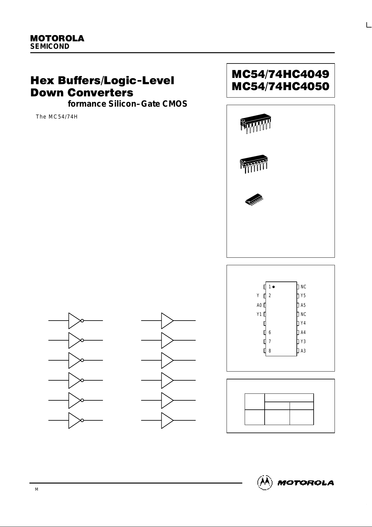
The M C54/74HC4049 c onsists o f six i nverting b uffers, a nd t he
MC54/74HC4050 consists of six noninverting buffers. They are identical in
pinout to the MC14049UB and MC14050B metal–gate CMOS buffers. The
device inputs are compatible with standard CMOS outputs; with pullup
resistors, they are compatible with LSTTL outputs.
The input p rotection circuitry on these devices has been modified by
eliminating the VCC diodes to allow the use of input voltages up to 15 volts.
Thus, the devices may be used as logic–level translators that convert from a
high voltage to a low voltage while operating at the low–voltage power
supply. They allow MC14000–series CMOS operating up to 15 volts to be
interfaced with High–Speed CMOS at 2 to 6 volts. The protection diodes to
GND are Zener diodes, which protect the inputs from both positive and
negative voltage transients.
• Output Drive Capability: 10 LSTTL Loads
• Outputs Directly Interface to CMOS, NMOS, and TTL
• Operating Voltage Range: 2 to 6 V
• Low Input Current: 5 µA
• High Noise Immunity Characteristic of CMOS Devices
• In Compliance with the Requirements Defined by JEDEC Standard
No. 7A
• Chip Complexity: 36 FETs or 9 Equivalent Gates (4049)
24 FETs or 6 Equivalent Gates (4050)
LOGIC DIAGRAMS
Y0A0
A1
A2
A3
A4
A5
Y1
Y2
Y3
Y4
Y5
7
9
11
14
2
4
6
10
12
15
PIN 1 = V
CC
PIN 8 = GND
PINS 13, 16 = NO CONNECTION
HC4049
(INVERTING BUFFER)
Y0A0
A1
A2
A3
A4
A5
Y1
Y2
Y3
Y4
Y5
7
9
11
14
2
4
6
10
12
15
HC4050
(NONINVERTING BUFFER)
5
3
PIN ASSIGNMENT
FUNCTION TABLE
13
14
15
16
9
10
11
125
4
3
2
1
8
7
6
Y4
NC
A5
Y5
NC
A3
Y3
A4
Y1
A0
Y0
V
CC
GND
A2
Y2
A1
A
Y Outputs
Input HC4049 HC4060
L H L
H L H
NC = NO CONNECTION
D SUFFIX
SOIC PACKAGE
CASE 751B–05
N SUFFIX
PLASTIC PACKAGE
CASE 648–08
ORDERING INFORMATION
MC54HCXXXXJ
MC74HCXXXXN
MC74HCXXXXD
Ceramic
Plastic
SOIC
1
16
1
16
J SUFFIX
CERAMIC PACKAGE
CASE 620–10
1
16
MC54/74HC4049 MC54/74HC4050
MOTOROLA High–Speed CMOS Logic Data
DL129 — Rev 6
2
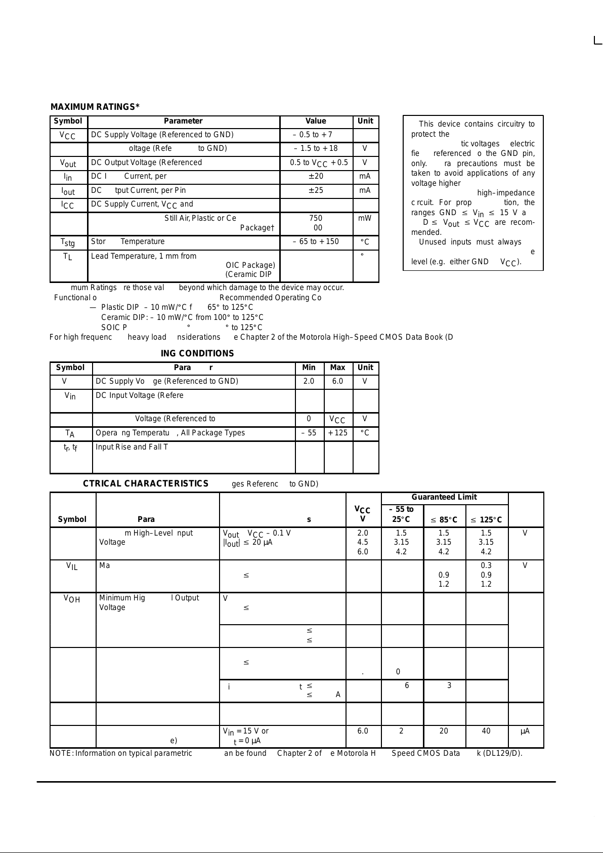
MAXIMUM RATINGS*
Symbol
Parameter
Value
Unit
V
CC
DC Supply Voltage (Referenced to GND)
– 0.5 to + 7.0
V
V
in
DC Input Voltage (Referenced to GND)
– 1.5 to + 18
V
V
out
DC Output Voltage (Referenced to GND)
– 0.5 to VCC + 0.5
V
I
in
DC Input Current, per Pin
± 20
mA
I
out
DC Output Current, per Pin
± 25
mA
I
CC
DC Supply Current, VCC and GND Pins
± 50
mA
P
D
Power Dissipation in Still Air,Plastic or Ceramic DIP†
SOIC Package†
750
500
mW
T
stg
Storage Temperature
– 65 to + 150
_
C
T
L
Lead Temperature, 1 mm from Case for 10 Seconds
(Plastic DIP or SOIC Package)
(Ceramic DIP)
260
300
_
C
*Maximum Ratings are those values beyond which damage to the device may occur.
Functional operation should be restricted to the Recommended Operating Conditions.
†Derating — Plastic DIP: – 10 mW/_C from 65_ to 125_C
Ceramic DIP: – 10 mW/_C from 100_ to 125_C
SOIC Package: – 7 mW/_C from 65_ to 125_C
For high frequency or heavy load considerations, see Chapter 2 of the Motorola High–Speed CMOS Data Book (DL129/D).
RECOMMENDED OPERATING CONDITIONS
Symbol
Parameter
Min
Max
Unit
V
CC
DC Supply Voltage (Referenced to GND)
2.0
6.0
V
V
in
DC Input Voltage (Referenced to GND)
0
V
CC
to 15
V
V
out
DC Output Voltage (Referenced to GND)
0
V
CC
V
T
A
Operating Temperature, All Package Types
– 55
+ 125
_
C
tr, t
f
Input Rise and Fall Time VCC = 2.0 V
(Figure 1) VCC = 4.5 V
VCC = 6.0 V
0
0
0
1000
500
400
ns
DC ELECTRICAL CHARACTERISTICS (Voltages Referenced to GND)
Guaranteed Limit
Symbol
Parameter
Test Conditions
V
CC
V
– 55 to
25_C
v
85_Cv 125_C
Unit
V
IH
Minimum High–Level Input
Voltage
V
out
= VCC – 0.1 V
|I
out
| v 20 µA
2.0
4.5
6.0
1.5
3.15
4.2
1.5
3.15
4.2
1.5
3.15
4.2
V
V
IL
Maximum Low–Level Input
Voltage
V
out
= 0.1 V or VCC – 0.1 V
|I
out
| v 20 µA
2.0
4.5
6.0
0.3
0.9
1.2
0.3
0.9
1.2
0.3
0.9
1.2
V
V
OH
Minimum High–Level Output
Voltage
Vin = V
IH
|I
out
| v 20 µA
2.0
4.5
6.0
1.9
4.4
5.9
1.9
4.4
5.9
1.9
4.4
5.9
V
Vin = VIH or VIL|I
out
| v 4.0 mA
|I
out
| v 5.2 mA
4.5
6.0
3.98
5.48
3.84
5.34
3.70
5.20
V
OL
Maximum Low–Level Output
Voltage
Vin = VIH or V
IL
|I
out
| v 20 µA
2.0
4.5
6.0
0.1
0.1
0.1
0.1
0.1
0.1
0.1
0.1
0.1
V
Vin = VIH or VIL|I
out
| v 4.0 mA
|I
out
| v 5.2 mA
4.5
6.0
0.26
0.26
0.33
0.33
0.40
0.40
I
in
Maximum Input Leakage Current
Vin = VCC or GND
Vin = 15 V
6.0
6.0
± 0.1
0.5
± 1.0
5.0
± 1.0
5.0
µA
I
CC
Maximum Quiescent Supply
Current (per Package)
Vin = 15 V or GND
I
out
= 0 µA
6.0
2
20
40
µA
NOTE: Information on typical parametric values can be found in Chapter 2 of the Motorola High–Speed CMOS Data Book (DL129/D).
This device contains circuitry to
protect the inputs against damage
due to high static voltages or electric
fields referenced to the GND pin,
only. Extra precautions must be
taken to avoid applications of any
voltage higher than maximum rated
voltages to this high–impedance
circuit. For proper operation, the
ranges GND v Vin v 15 V and
GND v V
out
v VCC are recom-
mended.
Unused inputs must always be
tied to an appropriate logic voltage
level (e.g., either GND or VCC).
 Loading...