

Motorola MC74HC4046AN, MC74HC4046AD Datasheet
SEMICONDUCTOR TECHNICAL DATA
3–1
REV 6
Motorola, Inc. 1995
10/95
High–Performance Silicon–Gate CMOS
The MC574HC4046A is similar in function to the MC14046 Metal gate
CMOS device. The device inputs are compatible with standard CMOS
outputs; with pullup resistors, they are compatible with LSTTL outputs.
The HC4046A phase–locked loop contains three phase comparators, a
voltage–controlled oscillator (VCO) and unity gain op–amp DEM
OUT
. The
comparators have two common signal inputs, COMPIN, and SIGIN. Input
SIGIN and COMPIN can be used directly coupled to large voltage signals, or
indirectly coupled (with a series capacitor to small voltage signals). The
self–bias circuit adjusts small voltage signals in the linear region of the
amplifier. Phase comparator 1 (an exclusive OR gate) provides a digital error
signal PC1
OUT
and m aintains 90 d egrees phase shift at the center
frequency between SIGIN and COMPIN signals (both at 50% duty cycle).
Phase comparator 2 (with leading–edge sensing logic) provides digital error
signals P C2
OUT
and P CP
OUT
and maintains a 0 degree phase shift
between SIGIN and COMPIN signals (duty cycle is immaterial). The linear
VCO produces an output signal VCO
OUT
whose frequency is determined by
the voltage of input VCOIN signal and the capacitor and resistors connected
to pins C1A, C1B, R1 and R2. The unity gain op–amp output DEM
OUT
with
an external resistor is used where the VCOIN signal is needed but no loading
can be tolerated. The inhibit input, when high, disables the VCO and all
op–amps to minimize standby power consumption.
Applications include FM and FSK modulation and demodulation, frequency synthesis and multiplication, frequency discrimination, tone decoding,
data synchronization and conditioning, voltage–to–frequency conversion
and motor speed control.
• Output Drive Capability: 10 LSTTL Loads
• Low Power Consumption Characteristic of CMOS Devices
• Operating Speeds Similar to LSTTL
• Wide Operating Voltage Range: 3.0 to 6.0 V
• Low Input Current: 1.0
µA Maximum (except SIG
IN
and COMPIN)
• In Compliance with the Requirements Defined by JEDEC Standard
No. 7A
• Low Quiescent Current: 80 µA Maximum (VCO disabled)
• High Noise Immunity Characteristic of CMOS Devices
• Diode Protection on all Inputs
• Chip Complexity: 279 FETs or 70 Equivalent Gates
Pin No. Symbol Name and Function
1
2
3
4
5
6
7
8
9
10
11
12
13
14
15
16
PCP
OUT
PC1
OUT
COMP
IN
VCO
OUT
INH
C1A
C1B
GND
VCO
IN
DEM
OUT
R1
R2
PC2
OUT
SIG
IN
PC3
OUT
V
CC
Phase Comparator Pulse Output
Phase Comparator 1 Output
Comparator Input
VCO Output
Inhibit Input
Capacitor C1 Connection A
Capacitor C1 Connection B
Ground (0 V) V
SS
VCO Input
Demodulator Output
Resistor R1 Connection
Resistor R2 Connection
Phase Comparator 2 Output
Signal Input
Phase Comparator 3 Output
Positive Supply Voltage
PIN ASSIGNMENT
D SUFFIX
SOIC PACKAGE
CASE 751B–05
N SUFFIX
PLASTIC PACKAGE
CASE 648–08
1
16
1
16
ORDERING INFORMATION
MC74HCXXXXAN
MC74HCXXXXAD
Plastic
SOIC
13
14
15
16
9
10
11
125
4
3
2
1
8
7
6
R2
PC2
out
SIG
in
PC3
out
V
CC
VCO
in
DEM
out
R1
VCO
out
COMP
in
PC1
out
PCP
out
GND
C1B
C1A
INH
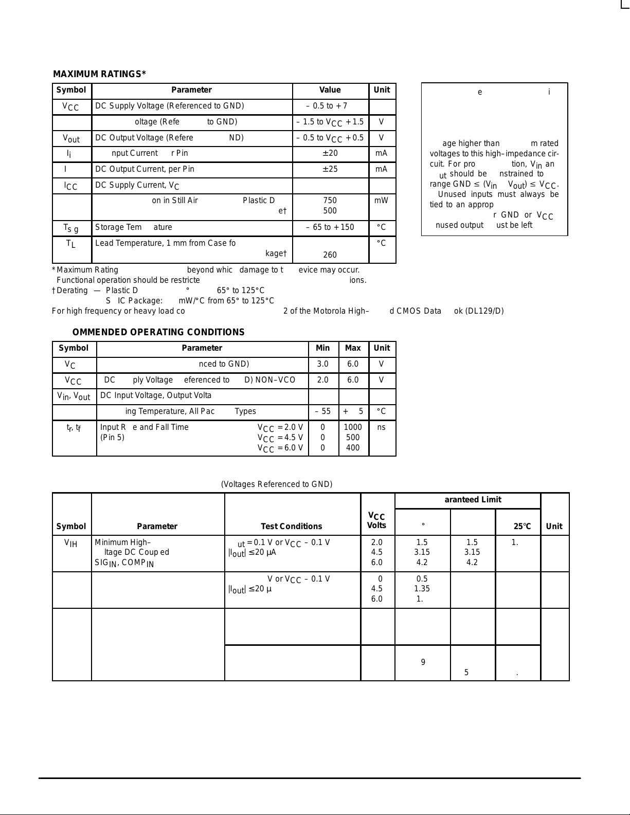
MC74HC4046A
MOTOROLA High–Speed CMOS Logic Data
DL129 — Rev 6
3–2
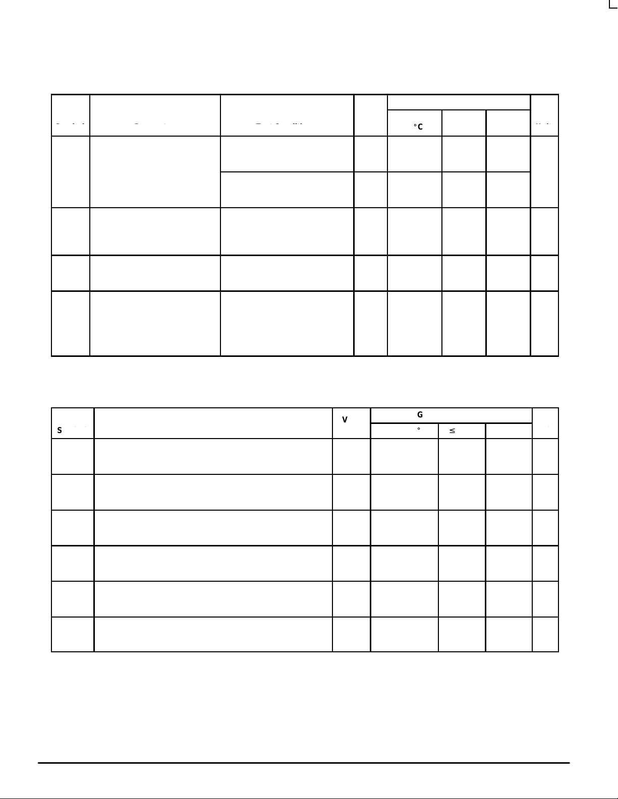
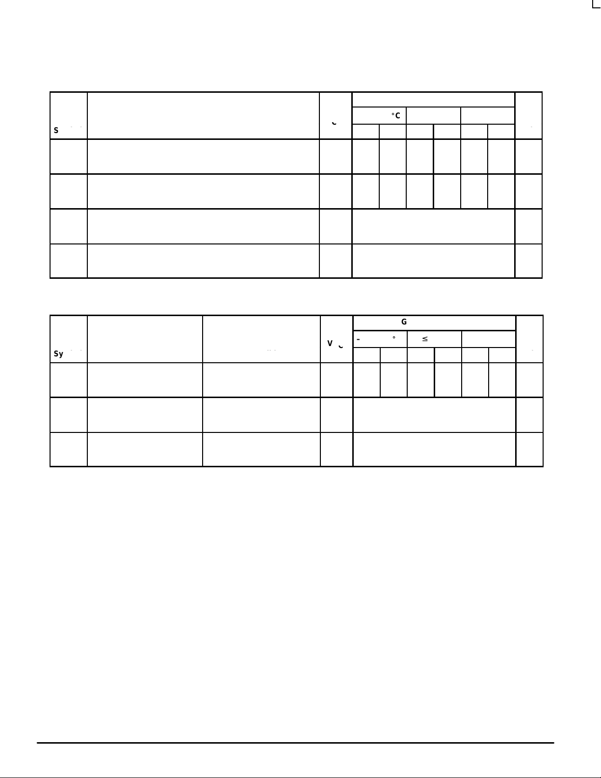
MAXIMUM RATINGS*
Symbol
Parameter
Value
Unit
V
CC
DC Supply Voltage (Referenced to GND)
– 0.5 to + 7.0
V
V
in
DC Input Voltage (Referenced to GND)
– 1.5 to VCC + 1.5
V
V
out
DC Output Voltage (Referenced to GND)
– 0.5 to VCC + 0.5
V
I
in
DC Input Current, per Pin
± 20
mA
I
out
DC Output Current, per Pin
± 25
mA
I
CC
DC Supply Current, VCC and GND Pins
± 50
mA
P
D
Power Dissipation in Still Air Plastic DIP†
SOIC Package†
750
500
mW
T
stg
Storage Temperature
– 65 to + 150
_
C
T
L
Lead Temperature, 1 mm from Case for 10 Seconds
Plastic DIP and SOIC Package†
260
_
C
*Maximum Ratings are those values beyond which damage to the device may occur.
Functional operation should be restricted to the Recommended Operating Conditions.
†Derating — Plastic DIP: – 10 mW/_C from 65_ to 125_C
SOIC Package: – 7 mW/_C from 65_ to 125_C
For high frequency or heavy load considerations, see Chapter 2 of the Motorola High–Speed CMOS Data Book (DL129/D).
RECOMMENDED OPERATING CONDITIONS
Symbol
Parameter
Min
Max
Unit
V
CC
DC Supply Voltage (Referenced to GND)
3.0
6.0
V
V
CC
DC Supply Voltage (Referenced to GND) NON–VCO 2.0 6.0 V
Vin, V
out
DC Input Voltage, Output Voltage (Referenced to GND)
0
V
CC
V
T
A
Operating Temperature, All Package Types
– 55
+ 125
_
C
tr, t
f
Input Rise and Fall Time VCC = 2.0 V
(Pin 5) VCC = 4.5 V
VCC = 6.0 V
0
0
0
1000
500
400
ns
[Phase Comparator Section]
DC ELECTRICAL CHARACTERISTICS
(Voltages Referenced to GND)
Guaranteed Limit
Symbol
Parameter
Test Conditions
V
CC
Volts
– 55 to
25_C
≤ 85°C
≤ 125°C
Unit
V
IH
Minimum High–Level Input
Voltage DC Coupled
SIGIN, COMP
IN
V
out
= 0.1 V or VCC – 0.1 V
|I
out
| ≤ 20 µA
2.0
4.5
6.0
1.5
3.15
4.2
1.5
3.15
4.2
1.5
3.15
4.2
V
V
IL
Maximum Low–Level Input
Voltage DC Coupled
SIGIN, COMP
IN
V
out
= 0.1 V or VCC – 0.1 V
|I
out
| ≤ 20 µA
2.0
4.5
6.0
0.5
1.35
1.8
0.5
1.35
1.8
0.5
1.35
1.8
V
V
OH
Minimum High–Level
Output Voltage
PCP
OUT
, PCn
OUT
Vin = VIH or V
IL
|I
out
| ≤ 20 µA
2.0
4.5
6.0
1.9
4.4
5.9
1.9
4.4
5.9
1.9
4.4
5.9
V
Vin = VIH or V
IL
|I
out
| ≤ 4.0 mA
|I
out
| ≤ 5.2 mA
4.5
6.0
3.98
5.48
3.84
5.34
3.7
5.2
(continued)
This device contains protection
circuitry to guard against damage
due to high static voltages or electric
fields. However, precautions must
be taken to avoid applications of any
voltage higher than maximum rated
voltages to this high–impedance circuit. For proper operation, Vin and
V
out
should be constrained to the
range GND v (Vin or V
out
) v VCC.
Unused inputs must always be
tied to an appropriate logic voltage
level (e.g., either GND or VCC).
Unused outputs must be left open.
MC74HC4046A
High–Speed CMOS Logic Data
DL129 — Rev 6
3–3 MOTOROLA
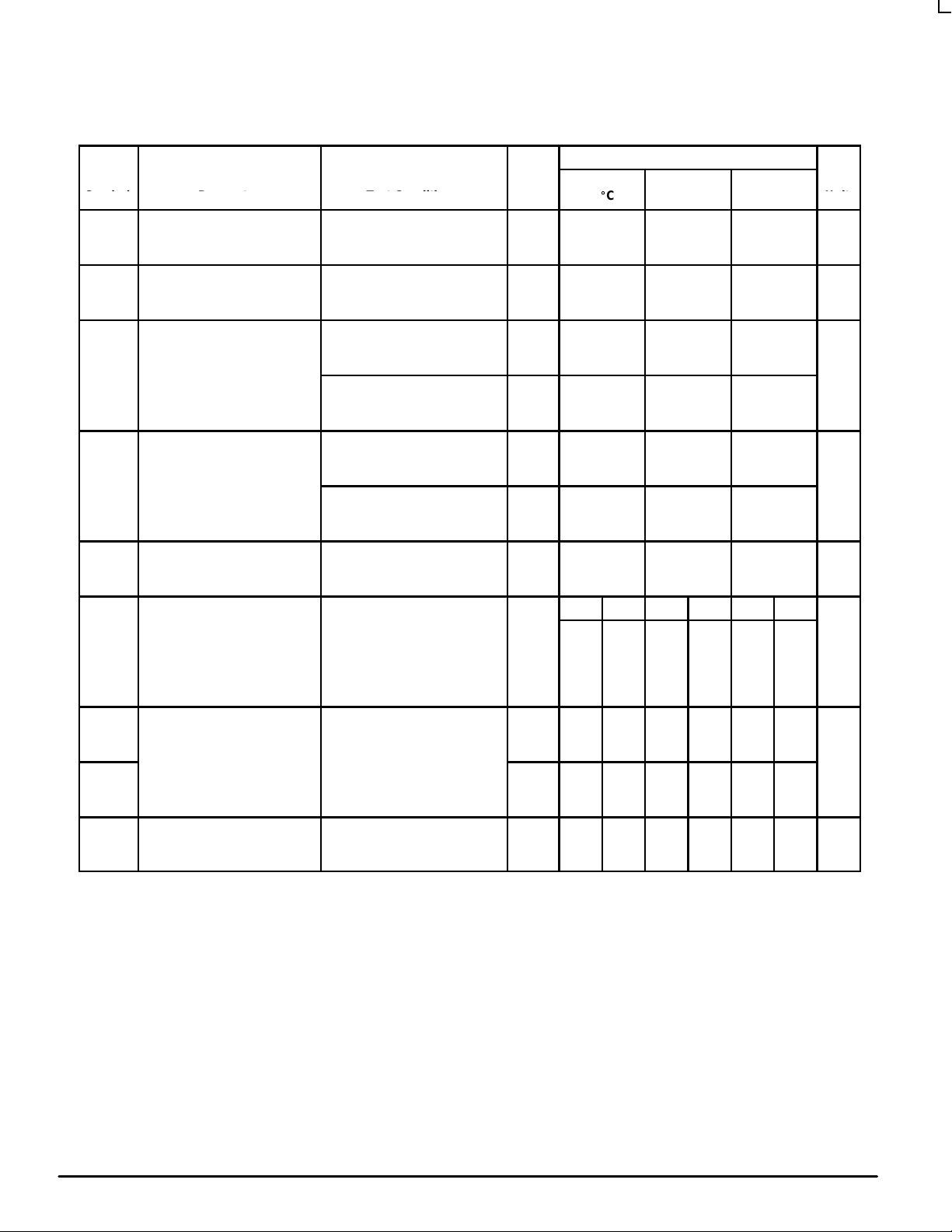
[Phase Comparator Section]
DC ELECTRICAL CHARACTERISTICS – continued
(Voltages Referenced to GND)
Guaranteed Limit
Symbol
Parameter
Test Conditions
V
CC
Volts
– 55 to
25_C
≤ 85°C
≤ 125°C
Unit
V
OL
Maximum Low–Level
Output Voltage Qa–Qh
PCP
OUT
, PCn
OUT
V
out
= 0.1 V or VCC – 0.1 V
|I
out
| ≤ 20 µA
2.0
4.5
6.0
0.1
0.1
0.1
0.1
0.1
0.1
0.1
0.1
0.1
V
Vin = VIH or V
IL
|I
out
| ≤ 4.0 mA
|I
out
| ≤ 5.2 mA
4.5
6.0
0.26
0.26
0.33
0.33
0.4
0.4
I
in
Maximum Input Leakage Current
SIGIN, COMP
IN
Vin = VCC or GND
2.0
3.0
4.5
6.0
± 3.0
± 7.0
± 18.0
± 30.0
± 4.0
± 9.0
± 23.0
± 38.0
± 5.0
± 11.0
± 27.0
± 45.0
µA
I
OZ
Maximum Three–State
Leakage Current
PC2
OUT
Output in High–Impedance State
Vin = VIH or V
IL
V
out
= VCC or GND
6.0 ± 0.5 ± 5.0 ± 10 µA
I
CC
Maximum Quiescent Supply
Current (per Package)
(VCO disabled)
Pins 3, 5 and 14 at V
CC
Pin 9 at GND; Input Leakage at
Pins 3 and 14 to be excluded
Vin = VCC or GND
|I
out
| = 0 µA
6.0 4.0 40 160 µA
NOTE: Information on typical parametric values can be found in Chapter 2 of the Motorola High–Speed CMOS Data Book (DL129/D).
[Phase Comparator Section]
AC ELECTRICAL CHARACTERISTICS
(CL = 50 pF, Input tr = tf = 6.0 ns)
Guaranteed Limit
Symbol
Parameter
V
CC
Volts
– 55 to 25_C
≤ 85°C ≤ 125°C
Unit
t
PLH
,
t
PHL
Maximum Propagation Delay, SIGIN/COMPIN to PC1
OUT
(Figure 1)
2.0
4.5
6.0
175
35
30
220
44
37
265
53
45
ns
t
PLH
,
t
PHL
Maximum Propagation Delay, SIGIN/COMPIN to PCP
OUT
(Figure 1)
2.0
4.5
6.0
340
68
58
425
85
72
510
102
87
ns
t
PLH
,
t
PHL
Maximum Propagation Delay, SIGIN/COMPIN to PC3
OUT
(Figure 1)
2.0
4.5
6.0
270
54
46
340
68
58
405
81
69
ns
t
PLZ
,
t
PHZ
Maximum Propagation Delay, SIGIN/COMPIN Output
Disable Time to PC2
OUT
(Figures 2 and 3)
2.0
4.5
6.0
200
40
34
250
50
43
300
60
51
ns
t
PZH
,
t
PZL
Maximum Propagation Delay, SIGIN/COMPIN Output
Enable Time to PC2
OUT
(Figures 2 and 3)
2.0
4.5
6.0
230
46
39
290
58
49
345
69
59
ns
t
TLH
,
t
THL
Maximum Output Transition Time
(Figure 1)
2.0
4.5
6.0
75
15
13
95
19
16
110
22
19
ns
MC74HC4046A
MOTOROLA High–Speed CMOS Logic Data
DL129 — Rev 6
3–4
[VCO Section]
DC ELECTRICAL CHARACTERISTICS
(Voltages Referenced to GND)
Guaranteed Limit
Symbol
Parameter
Test Conditions
V
CC
Volts
– 55 to
25_C
≤ 85°C
≤ 125°C
Unit
V
IH
Minimum High–Level
Input Voltage
INH
V
out
= 0.1 V or VCC – 0.1 V
|I
out
| ≤ 20 µA
3.0
4.5
6.0
2.1
3.15
4.2
2.1
3.15
4.2
2.1
3.15
4.2
V
V
IL
Maximum Low–Level
Input Voltage
INH
V
out
= 0.1 V or VCC – 0.1 V
|I
out
| ≤ 20 µA
3.0
4.5
6.0
0.90
1.35
1.8
0.9
1.35
1.8
0.9
1.35
1.8
V
V
OH
Minimum High–Level
Output Voltage
VCO
OUT
Vin= VIH or V
IL
|I
out
| ≤ 20 µA
3.0
4.5
6.0
1.9
4.4
5.9
1.9
4.4
5.9
1.9
4.4
5.9
V
Vin= VIH or V
IL
|I
out
| ≤ 4.0 mA
|I
out
| ≤ 5.2 mA
4.5
6.0
3.98
5.48
3.84
5.34
3.7
5.2
V
OL
Maximum Low–Level
Output Voltage
VCO
OUT
V
out
= 0.1 V or VCC – 0.1 V
|I
out
| ≤ 20 µA
3.0
4.5
6.0
0.1
0.1
0.1
0.1
0.1
0.1
0.1
0.1
0.1
V
Vin= VIH or V
IL
|I
out
| ≤ 4.0 mA
|I
out
| ≤ 5.2 mA
4.5
6.0
0.26
0.26
0.33
0.33
0.4
0.4
I
in
Maximum Input
Leakage Current
INH, VCO
IN
Vin= VCC or GND 6.0 0.1 1.0 1.0 µA
Min Max Min Max Min Max
Operating Voltage Range at
VCOIN over the range
specified for R1; For linearity
see Fig. 15A, Parallel value of
R1 and R2 should be > 2.7 kΩ
INH = V
IL
3.0
4.5
6.0
0.1
0.1
0.1
1.0
2.5
4.0
0.1
0.1
0.1
1.0
2.5
4.0
0.1
0.1
0.1
1.0
2.5
4.0
V
R1 Resistor Range 3.0
4.5
6.0
3.0
3.0
3.0
300
300
300
3.0
3.0
3.0
300
300
300
3.0
3.0
3.0
300
300
300
kΩ
R2 3.0
4.5
6.0
3.0
3.0
3.0
300
300
300
3.0
3.0
3.0
300
300
300
3.0
3.0
3.0
300
300
300
C1 Capacitor Range 3.0
4.5
6.0
40
40
40
No
Limit
pF
V
VCO
IN
MC74HC4046A
High–Speed CMOS Logic Data
DL129 — Rev 6
3–5 MOTOROLA
[VCO Section]
AC ELECTRICAL CHARACTERISTICS
(CL = 50 pF, Input tr = tf = 6.0 ns)
Guaranteed Limit
V
– 55 to 25_C
≤ 85°C
≤ 125°C
Symbol
Parameter
V
CC
Volts
Min Max Min Max Min Max
Unit
∆f/T Frequency Stability with
Temperature Changes
(Figure 13A, B, C)
3.0
4.5
6.0
%/K
fo VCO Center Frequency
(Duty Factor = 50%)
(Figure 14A, B, C, D)
3.0
4.5
6.0
3
11
13
MHz
∆fVCO VCO Frequency Linearity 3.0
4.5
6.0
See Figures 15A, B, C %
∂ VCO Duty Factor at VCO
OUT
3.0
4.5
6.0
Typical 50% %
[Demodulator Section]
DC ELECTRICAL CHARACTERISTICS
Guaranteed Limit
V
– 55 to 25_C
≤ 85°C
≤ 125°C
Symbol
Parameter
Test Conditions
V
CC
Volts
Min Max Min Max Min Max
Unit
RS Resistor Range At RS > 300 kΩ the
Leakage Current can
Influence VDEM
OUT
3.0
4.5
6.0
50
50
50
300
300
300
kΩ
V
OFF
Offset Voltage
VCOIN to VDEM
OUT
Vi = VVCOIN = 1/2 VCC;
Values taken over RS
Range.
3.0
4.5
6.0
See Figure 12 mV
RD Dynamic Output
Resistance at DEM
OUT
VDEM
OUT
= 1/2 V
CC
3.0
4.5
6.0
Typical 25 Ω Ω
 Loading...