

MOTOROLA MC74HC244AH, MC74HC244AFR1, MC74HC244ADWR2, MC74HC244AF, MC74HC244AFL1 Datasheet
...
Semiconductor Components Industries, LLC, 2000
March, 2000 – Rev. 8
1 Publication Order Number:
MC74HC244A/D
MC74HC244A
Octal 3-State Noninverting
Buffer/Line Driver/
Line Receiver
High–Performance Silicon–Gate CMOS
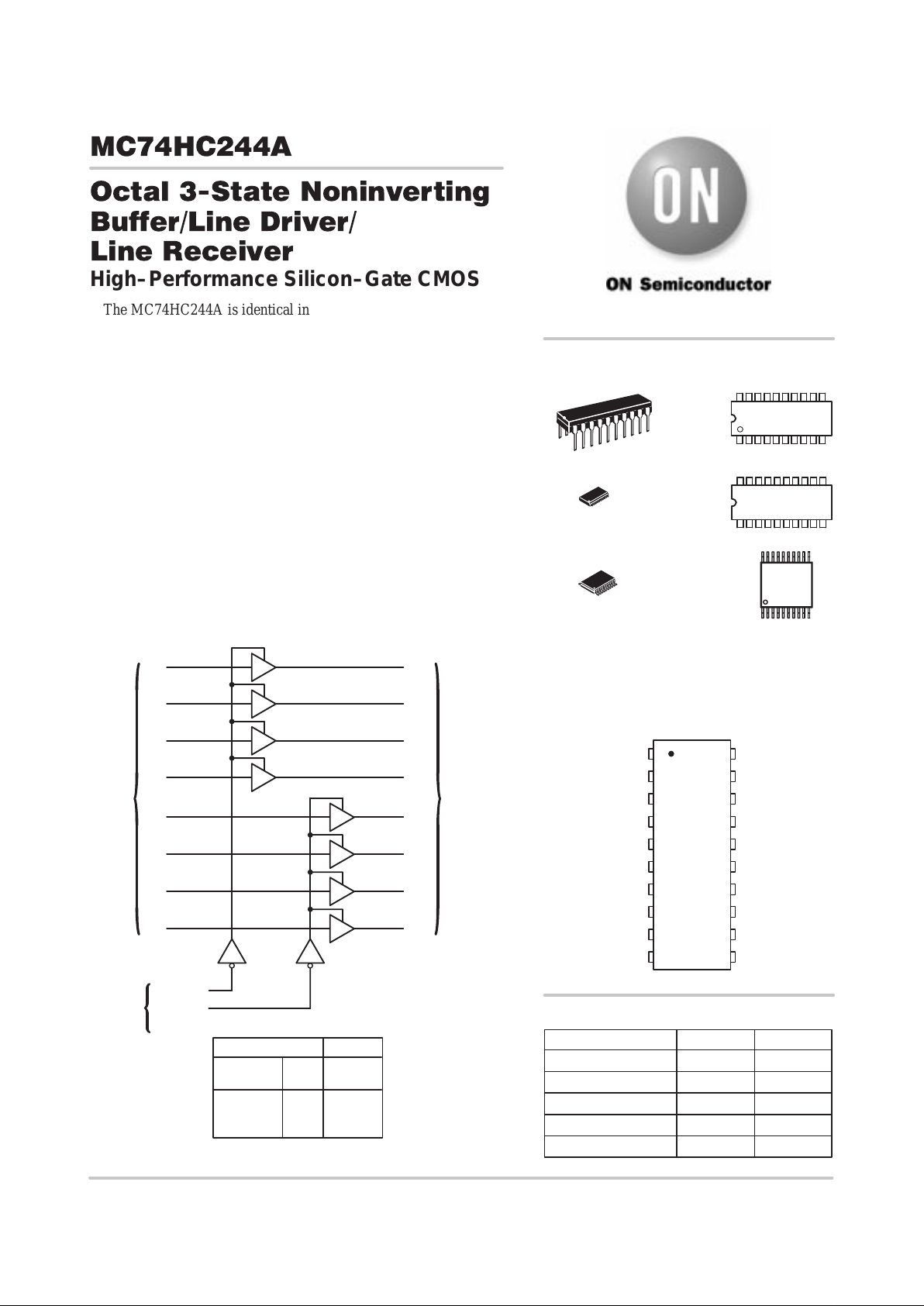
The MC74HC244A is identical in pinout to the LS244. The device
inputs are compatible with standard CMOS outputs; with pullup
resistors, they are compatible with LSTTL outputs.
This octal noninverting buffer/line driver/line receiver is designed
to be used with 3–state memory address drivers, clock drivers, and
other bus–oriented systems. The device has noninverting outputs and
two active–low output enables.
The HC244A is similar in function to the HC240A.
• Output Drive Capability: 15 LSTTL Loads
• Outputs Directly Interface to CMOS, NMOS, and TTL
• Operating Voltage Range: 2 to 6 V
• Low Input Current: 1 µA
• High Noise Immunity Characteristic of CMOS Devices
• In Compliance with the Requirements Defined by JEDEC Standard
No. 7A
• Chip Complexity: 136 FETs or 34 Equivalent Gates
LOGIC DIAGRAM
DATA
INPUTS
A1
A2
A3
A4
B1
B2
B3
B4
17
15
13
11
8
6
4
218
16
14
12
9
7
5
3
YB4
YB3
YB2
YB1
YA4
YA3
YA2
YA1
NONINVERTING
OUTPUTS
PIN 20 = V
CC
PIN 10 = GND
OUTPUT
ENABLES
ENABLE A
ENABLE B
1
19
FUNCTION TABLE
Inputs Outputs
Enable A,
Enable B A, B YA, YB
LLL
LHH
HXZ
Z = high impedance
http://onsemi.com
MARKING
DIAGRAMS
1
20
A = Assembly Location
WL = Wafer Lot
YY = Year
WW = Work Week
SOIC WIDE–20
DW SUFFIX
CASE 751D
HC244A
AWLYYWW
PDIP–20
N SUFFIX
CASE 738
1
20
MC74HC244AN
AWLYYWW
TSSOP–20
DT SUFFIX
CASE 948G
1
20
1
20
1
20
Device Package Shipping
ORDERING INFORMATION
MC74HC244AN PDIP–20 1440 / Box
MC74HC244ADW SOIC–WIDE
38 / Rail
MC74HC244ADWR2 SOIC–WIDE 1000 / Reel
MC74HC244ADT TSSOP–20 75 / Rail
MC74HC244ADTR2 TSSOP–20
2500 / Reel
HC
244A
ALYW
1
20
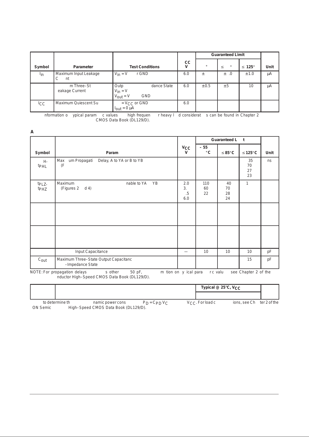
PIN ASSIGNMENT
A3
A2
YB4
A1
ENABLE A
GND
YB1
A4
YB2
YB3 5
4
3
2
1
10
9
8
7
6
14
15
16
17
18
19
20
11
12
13
YA2
B4
YA1
ENABLE B
V
CC
B1
YA4
B2
YA3
B3
MC74HC244A
http://onsemi.com
2
MAXIMUM RATINGS*
Symbol
Parameter
Value
Unit
V
CC
DC Supply Voltage (Referenced to GND)
– 0.5 to + 7.0
V
V
in
DC Input Voltage (Referenced to GND)
– 0.5 to VCC + 0.5
V
V
out
DC Output Voltage (Referenced to GND)
– 0.5 to VCC + 0.5
V
I
in
DC Input Current, per Pin
± 20
mA
I
out
DC Output Current, per Pin
± 35
mA
I
CC
DC Supply Current, VCC and GND Pins
± 75
mA
ÎÎ
Î
P
D
ОООООООООООО
Î
Power Dissipation in Still Air, Plastic DIP†
SOIC Package†
TSSOP Package†
ÎÎÎ
Î
750
500
450
Î
Î
mW
T
stg
Storage Temperature
– 65 to + 150
_
C
ÎÎ
Î
T
L
ОООООООООООО
Î
Lead Temperature, 1 mm from Case for 10 Seconds
(Plastic DIP, SOIC, SSOP or TSSOP Package)
ÎÎÎ
Î
260
Î
Î
_
C
*Maximum Ratings are those values beyond which damage to the device may occur.
Functional operation should be restricted to the Recommended Operating Conditions.
†Derating — Plastic DIP: – 10 mW/_C from 65_ to 125_C
SOIC Package: – 7 mW/_C from 65_ to 125_C
TSSOP Package: – 6.1 mW/_C from 65_ to 125_C
For high frequency or heavy load considerations, see Chapter 2 of the ON Semiconductor High–Speed CMOS Data Book (DL129/D).
RECOMMENDED OPERATING CONDITIONS
Symbol
Parameter
Min
ÎÎ
Max
Unit
V
CC
DC Supply Voltage (Referenced to GND)
2.0
ÎÎ
6.0
V
Vin, V
out
DC Input Voltage, Output Voltage (Referenced to GND)
0
ÎÎ
V
CC
V
T
A
Operating Temperature, All Package Types
– 55
ÎÎ
+ 125
_
C
ÎÎ
Î
tr, t
f
ООООООООООООО
Î
Input Rise and Fall Time VCC = 2.0 V
(Figure 1) VCC = 4.5 V
VCC = 6.0 V
Î
Î
0
0
0
ÎÎ
ÎÎ
1000
500
400
Î
Î
ns
DC ELECTRICAL CHARACTERISTICS (Voltages Referenced to GND)
Guaranteed Limit
ÎÎ
Î
Symbol
ООООООО
Î
Parameter
ООООООО
Î
Test Conditions
ÎÎ
Î
V
CC
V
ÎÎ
Î
– 55 to
25_C
ÎÎÎ
Î
Î
Î
v
85_C
ÎÎ
Î
v
125_C
Î
Î
Unit
ÎÎ
Î
ÎÎ
Î
V
IH
ООООООО
Î
ООООООО
Î
Minimum High–Level Input
Voltage
ООООООО
Î
ООООООО
Î
V
out
= VCC – 0.1 V
|I
out
| v 20 µA
ÎÎ
Î
ÎÎ
Î
2.0
3.0
4.5
6.0
ÎÎ
Î
ÎÎ
Î
1.5
2.1
3.15
4.2
ÎÎÎ
Î
Î
Î
Î
Î
Î
1.5
2.1
3.15
4.2
ÎÎ
Î
ÎÎ
Î
1.5
2.1
3.15
4.2
Î
Î
Î
Î
V
ÎÎ
Î
ÎÎ
Î
V
IL
ООООООО
Î
ООООООО
Î
Maximum Low–Level Input
Voltage
ООООООО
Î
ООООООО
Î
V
out
= 0.1 V
|I
out
| v 20 µA
ÎÎ
Î
ÎÎ
Î
2.0
3.0
4.5
6.0
ÎÎ
Î
ÎÎ
Î
0.5
0.9
1.35
1.8
ÎÎÎ
Î
Î
Î
Î
Î
Î
0.5
0.9
1.35
1.8
ÎÎ
Î
ÎÎ
Î
0.5
0.9
1.35
1.8
Î
Î
Î
Î
V
ÎÎ
Î
V
OH
ООООООО
Î
Minimum High–Level Output
Voltage
ООООООО
Î
Vin = V
IH
|I
out
| v 20 µA
ÎÎ
Î
2.0
4.5
6.0
ÎÎ
Î
1.9
4.4
5.9
ÎÎÎ
Î
Î
Î
1.9
4.4
5.9
ÎÎ
Î
1.9
4.4
5.9
Î
Î
V
ÎÎÎОООООООÎООООООО
Î
Vin = V
IH
|I
out
| v 2.4 mA
|I
out
| v 6.0 mA
|I
out
| v 7.8 mA
ÎÎ
Î
3.0
4.5
6.0
ÎÎ
Î
2.48
3.98
5.48
ÎÎÎ
Î
Î
Î
2.34
3.84
5.34
ÎÎ
Î
2.2
3.7
5.2
Î
Î
ÎÎ
Î
V
OL
ООООООО
Î
Maximum Low–Level Output
Voltage
ООООООО
Î
Vin = V
IL
|I
out
| v 20 µA
ÎÎ
Î
2.0
4.5
6.0
ÎÎ
Î
0.1
0.1
0.1
ÎÎÎ
Î
Î
Î
0.1
0.1
0.1
ÎÎ
Î
0.1
0.1
0.1
Î
Î
V
ÎÎÎОООООООÎООООООО
Î
Vin = V
IL
|I
out
| v 2.4 mA
|I
out
| v 6.0 mA
|I
out
| v 7.8 mA
ÎÎ
Î
3.0
4.5
6.0
ÎÎ
Î
0.26
0.26
0.26
ÎÎÎ
Î
Î
Î
0.33
0.33
0.33
ÎÎ
Î
0.4
0.4
0.4
Î
Î
This device contains protection
circuitry to guard against damage
due to high static voltages or electric
fields. However, precautions must
be taken to avoid applications of any
voltage higher than maximum rated
voltages to this high–impedance circuit. For proper operation, Vin and
V
out
should be constrained to the
range GND v (Vin or V
out
) v VCC.
Unused inputs must always be
tied to an appropriate logic voltage
level (e.g., either GND or VCC).
Unused outputs must be left open.
MC74HC244A
http://onsemi.com
3
DC ELECTRICAL CHARACTERISTICS (Voltages Referenced to GND)
Guaranteed Limit
Unit
v
125_C
ÎÎÎ
v
85_C
– 55 to
25_C
V
CC
V
Test Conditions
Parameter
Symbol
ÎÎ
Î
I
in
ООООООО
Î
Maximum Input Leakage
Current
ООООООО
Î
Vin = VCC or GND
ÎÎ
Î
6.0
ÎÎ
Î
± 0.1
ÎÎÎ
Î
Î
Î
± 1.0
ÎÎ
Î
± 1.0
Î
Î
µA
ÎÎ
Î
I
OZ
ООООООО
Î
Maximum Three–State
Leakage Current
ООООООО
Î
Output in High–Impedance State
Vin = VIL or V
IH
V
out
= VCC or GND
ÎÎ
Î
6.0
ÎÎ
Î
± 0.5
ÎÎÎ
Î
Î
Î
± 5.0
ÎÎ
Î
± 10
Î
Î
µA
ÎÎ
Î
I
CC
ООООООО
Î
Maximum Quiescent Supply
Current (per Package)
ООООООО
Î
Vin = VCC or GND
I
out
= 0 µA
ÎÎ
Î
6.0
ÎÎ
Î
4.0
ÎÎÎ
Î
Î
Î
40
ÎÎ
Î
160
Î
Î
µA
NOTE: Infor mation o n typi cal par ametric value s and high frequency or heavy load considerations can b e found in Chapter 2 of the ON
Semiconductor High–Speed CMOS Data Book (DL129/D).
AC ELECTRICAL CHARACTERISTICS (C
L
= 50 pF, Input tr = tf = 6 ns)
Guaranteed Limit
Symbol
Parameter
V
CC
V
– 55 to
25_C
ÎÎÎ
v85_Cv
125_C
Unit
ÎÎÎ
Î
ÎÎÎ
Î
t
PLH
,
t
PHL
ОООООООООООООО
Î
ОООООООООООООО
Î
Maximum Propagation Delay, A to YA or B to YB
(Figures 1 and 3)
ÎÎ
Î
ÎÎ
Î
2.0
3.0
4.5
6.0
ÎÎ
Î
ÎÎ
Î
96
50
18
15
ÎÎÎ
Î
Î
Î
Î
Î
Î
115
60
23
20
ÎÎ
Î
ÎÎ
Î
135
70
27
23
Î
Î
Î
Î
ns
ÎÎÎ
Î
ÎÎÎ
Î
t
PLZ
,
t
PHZ
ОООООООООООООО
Î
ОООООООООООООО
Î
Maximum Propagation Delay, Output Enable to YA or YB
(Figures 2 and 4)
ÎÎ
Î
ÎÎ
Î
2.0
3.0
4.5
6.0
ÎÎ
Î
ÎÎ
Î
110
60
22
19
ÎÎÎ
Î
Î
Î
Î
Î
Î
140
70
28
24
ÎÎ
Î
ÎÎ
Î
165
80
33
28
Î
Î
Î
Î
ns
ÎÎÎ
Î
ÎÎÎ
Î
t
PZL
,
t
PZH
ОООООООООООООО
Î
ОООООООООООООО
Î
Maximum Propagation Delay, Output Enable to YA or YB
(Figures 2 and 4)
ÎÎ
Î
ÎÎ
Î
2.0
3.0
4.5
6.0
ÎÎ
Î
ÎÎ
Î
110
60
22
19
ÎÎÎ
Î
Î
Î
Î
Î
Î
140
70
28
24
ÎÎ
Î
ÎÎ
Î
165
80
33
28
Î
Î
Î
Î
ns
ÎÎÎ
Î
ÎÎÎ
Î
t
TLH
,
t
THL
ОООООООООООООО
Î
ОООООООООООООО
Î
Maximum Output Transition Time, Any Output
(Figures 1 and 3)
ÎÎ
Î
ÎÎ
Î
2.0
3.0
4.5
6.0
ÎÎ
Î
ÎÎ
Î
60
23
12
10
ÎÎÎ
Î
Î
Î
Î
Î
Î
75
27
15
13
ÎÎ
Î
ÎÎ
Î
90
32
18
15
Î
Î
Î
Î
ns
C
in
Maximum Input Capacitance
—
10
ÎÎÎ
10
10
pF
ÎÎÎ
Î
C
out
ОООООООООООООО
Î
Maximum Three–State Output Capacitance (Output in
High–Impedance State)
ÎÎ
Î
—
ÎÎ
Î
15
ÎÎÎ
Î
Î
Î
15
ÎÎ
Î
15
Î
Î
pF
NOTE: For propagation delays with loads other than 50 pF, and information on typical parametric values, see Chapter 2 of the ON
Semiconductor High–Speed CMOS Data Book (DL129/D).
Typical @ 25°C, VCC = 5.0 V
C
PD
Power Dissipation Capacitance (Per Buffer)*
34
pF
*Used to determine the no–load dynamic power consumption: PD = CPD V
CC
2
f + ICC VCC. For load considerations, see Chapter 2 of the
ON Semiconductor High–Speed CMOS Data Book (DL129/D).
 Loading...