

Motorola MC74HC00AN, MC74HC00ADT, MC74HC00AD Datasheet
SEMICONDUCTOR TECHNICAL DATA
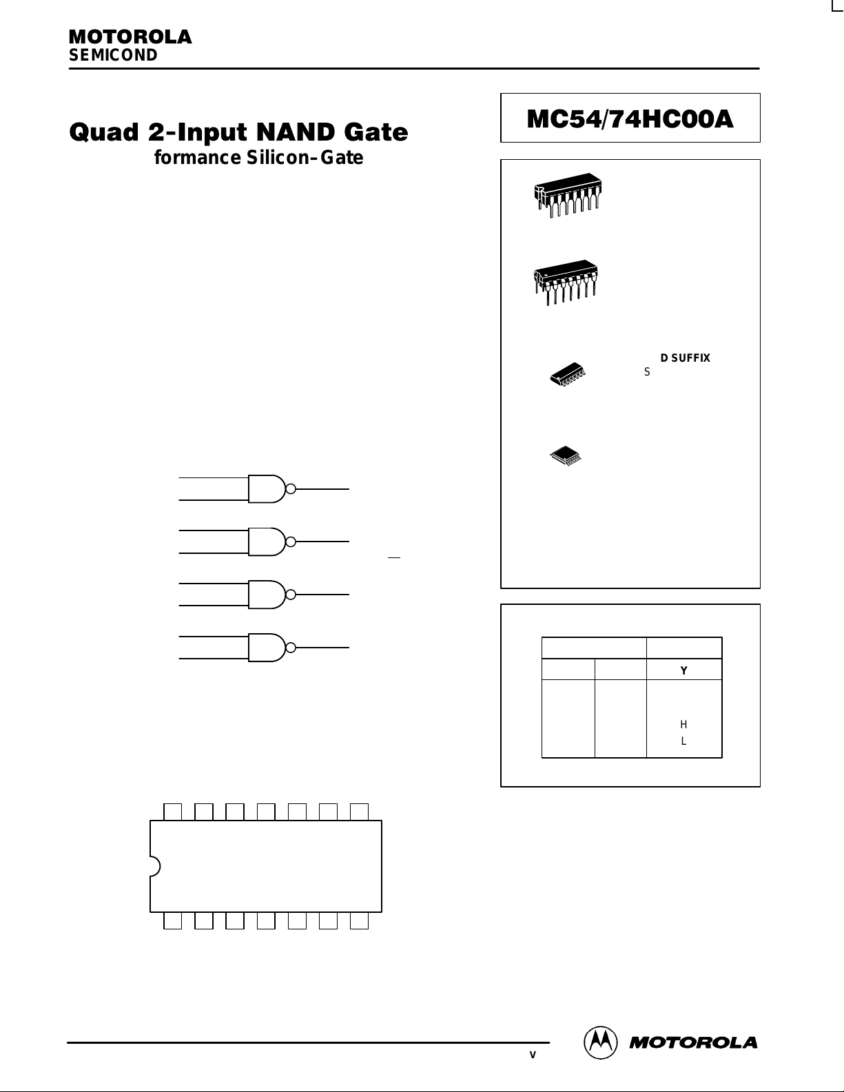
High–Performance Silicon–Gate CMOS
The MC54/74HC00A is identical in pinout to the LS00. The device
inputs are compatible with Standard CMOS outputs; with pullup resistors,
they are compatible with LSTTL outputs.
• Output Drive Capability: 10 LSTTL Loads
• Outputs Directly Interface to CMOS, NMOS and TTL
• Operating Voltage Range: 2 to 6V
• Low Input Current: 1µA
• High Noise Immunity Characteristic of CMOS Devices
• In Compliance With the JEDEC Standard No. 7A Requirements
• Chip Complexity: 32 FETs or 8 Equivalent Gates
LOGIC DIAGRAM
1
A1
2
B1
4
A2
5
B2
9
A3
10
B3
12
A4
13
B4
PIN 14 = V
PIN 7 = GND
CC
Pinout: 14–Lead Packages (Top View)
3
Y1
6
Y2
Y = AB
8
Y3
11
Y4
J SUFFIX
14
1
14
1
14
1
14
1
ORDERING INFORMATION
MC54HCXXAJ
MC74HCXXAN
MC74HCXXAD
MC74HCXXADT
FUNCTION TABLE
Inputs Output
AB
L
L
H
H
CERAMIC PACKAGE
CASE 632–08
N SUFFIX
PLASTIC PACKAGE
CASE 646–06
D SUFFIX
SOIC PACKAGE
CASE 751A–03
DT SUFFIX
TSSOP PACKAGE
CASE 948G–01
Ceramic
Plastic
SOIC
TSSOP
Y
L
H
L
H
H
H
H
L
10/95
Motorola, Inc. 1995
VCCB4 A4 Y4 B3 A3 Y3
1314 12 11 10 9 8
21 34567
A1 B1 Y1 A2 B2 Y2 GND
1
REV 7
MC54/74HC00A
Î
Î
Î
Î
Î
Î
Î
Î
Î
Î
Î
Î
Î
Î
Î
Î
Î
Î
Î
Î
Î
Î
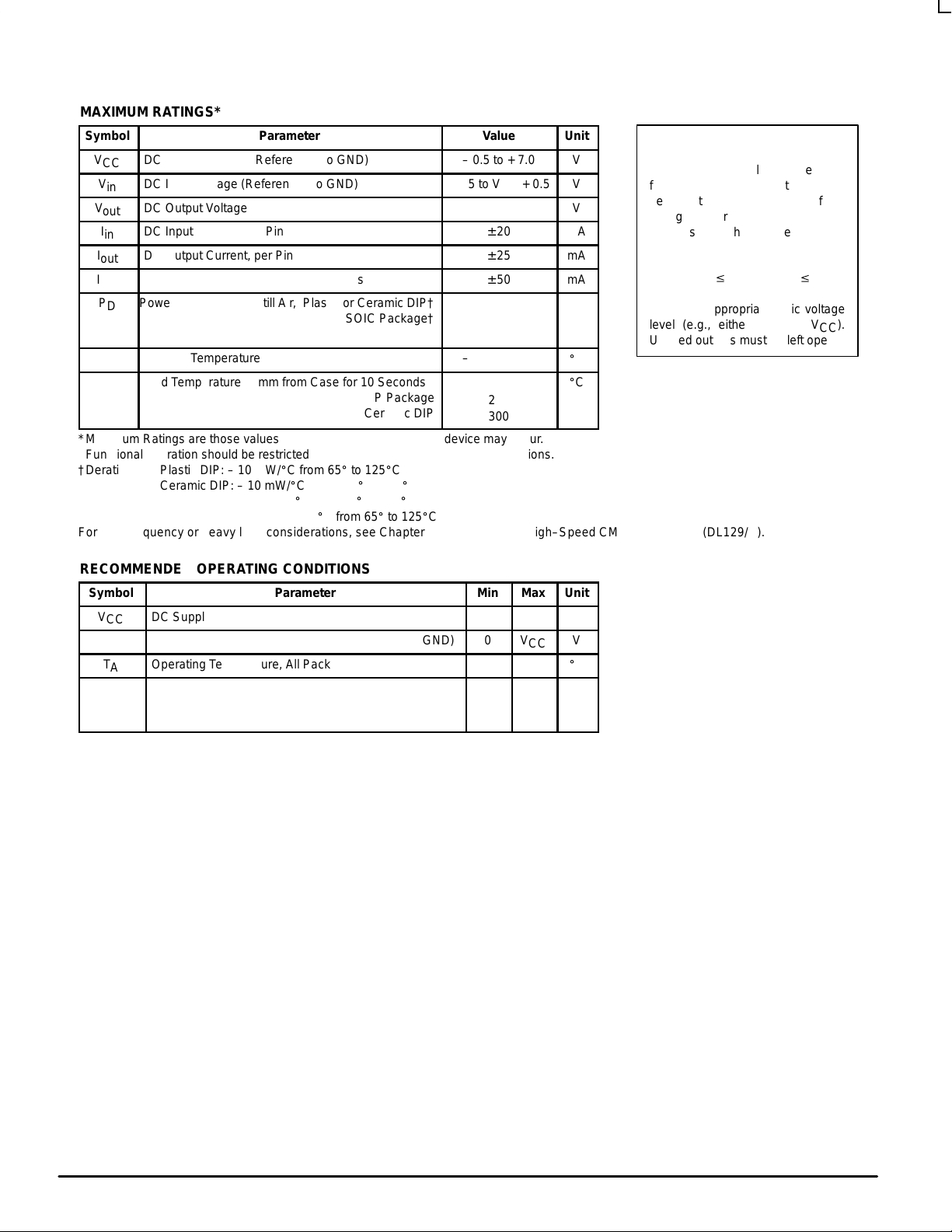
MAXIMUM RATINGS*
Symbol
V
V
I
I
Î
Î
T
Î
Î
Î
DC Supply Voltage (Referenced to GND)
CC
V
DC Input Voltage (Referenced to GND)
in
DC Output Voltage (Referenced to GND)
out
I
DC Input Current, per Pin
in
DC Output Current, per Pin
out
DC Supply Current, VCC and GND Pins
CC
P
Power Dissipation in Still Air, Plastic or Ceramic DIP†
D
ОООООООООООО
ОООООООООООО
Storage Temperature
stg
ОООООООООООО
T
Lead Temperature, 1 mm from Case for 10 Seconds
L
ОООООООООООО
ОООООООООООО
*Maximum Ratings are those values beyond which damage to the device may occur.
Functional operation should be restricted to the Recommended Operating Conditions.
†Derating — Plastic DIP: – 10 mW/_C from 65_ to 125_C
Ceramic DIP: – 10 mW/_C from 100_ to 125_C
SOIC Package: – 7 mW/_C from 65_ to 125_C
TSSOP Package: – 6.1 mW/_C from 65_ to 125_C
For high frequency or heavy load considerations, see Chapter 2 of the Motorola High–Speed CMOS Data Book (DL129/D).
Parameter
SOIC Package†
TSSOP Package†
Plastic DIP, SOIC or TSSOP Package
Ceramic DIP
Value
– 0.5 to + 7.0
– 0.5 to VCC + 0.5
– 0.5 to VCC + 0.5
± 20
± 25
± 50
750
500
ÎÎÎÎ
450
ÎÎÎÎ
– 65 to + 150
ÎÎÎÎ
ÎÎÎÎ
260
ÎÎÎÎ
300
Unit
V
V
V
mA
mA
mA
mW
Î
Î
_
C
Î
_
C
Î
Î
This device contains protection
circuitry to guard against damage
due to high static voltages or electric
fields. However, precautions must
be taken to avoid applications of any
voltage higher than maximum rated
voltages to this high–impedance circuit. For proper operation, Vin and
V
should be constrained to the
out
range GND v (Vin or V
Unused inputs must always be
tied to an appropriate logic voltage
level (e.g., either GND or VCC).
Unused outputs must be left open.
) v VCC.
out
RECOMMENDED OPERATING CONDITIONS
Symbol
V
CC
Vin, V
T
A
tr, t
ÎÎ
ÎÎ
DC Supply Voltage (Referenced to GND)
DC Input Voltage, Output Voltage (Referenced to GND)
out
Operating Temperature, All Package Types
Input Rise and Fall Time VCC = 2.0 V
f
ОООООООООООО
(Figure 1) VCC = 4.5 V
ОООООООООООО
Parameter
VCC = 6.0 V
Min
2.0
0
– 55
0
Î
0
0
Î
Max
6.0
V
CC
+ 125
1000
Î
500
400
Î
Unit
V
V
_
C
ns
Î
Î
MOTOROLA High–Speed CMOS Logic Data
2
DL129 — Rev 6
MC54/74HC00A
V
CC
V
CC
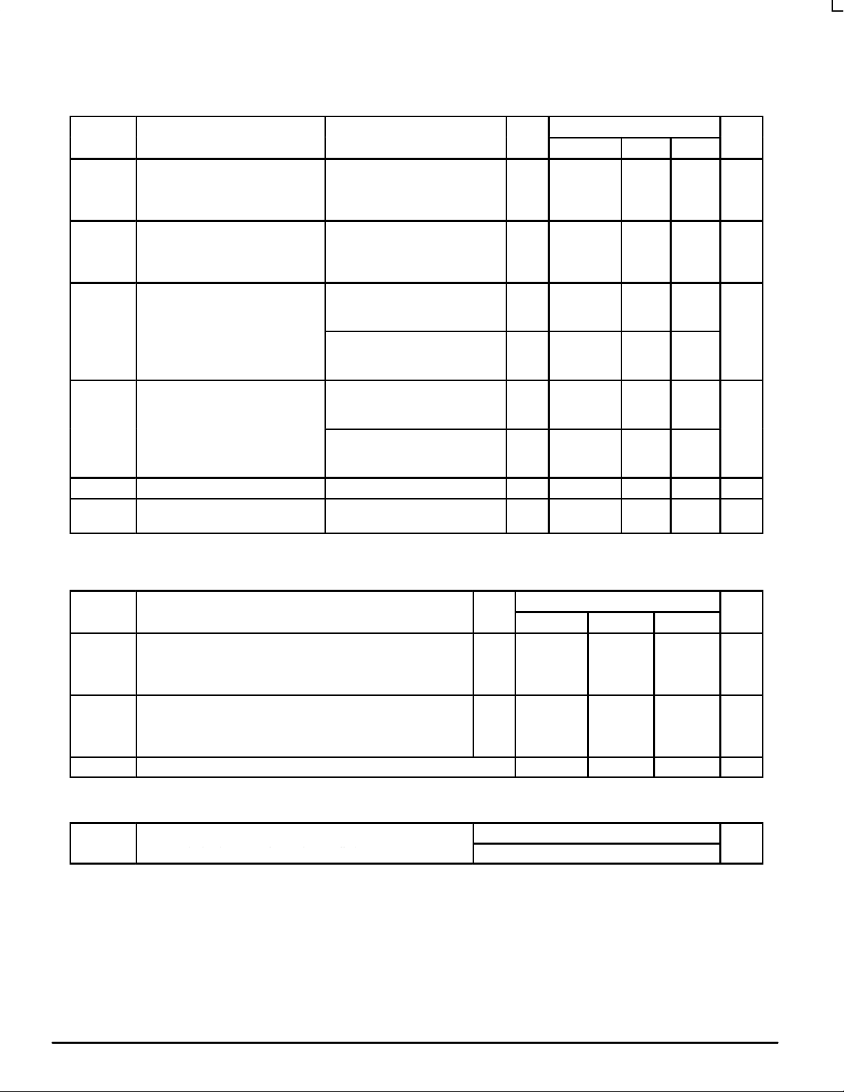
DC CHARACTERISTICS (Voltages Referenced to GND)
V
Symbol Parameter Condition
V
IH
V
IL
V
OH
V
OL
I
in
I
CC
NOTE:Information on typical parametric values can be found in Chapter 2 of the Motorola High–Speed CMOS Data Book (DL129/D).
Minimum High–Level Input Voltage V
Maximum Low–Level Input Voltage V
Minimum High–Level Output
Voltage
Maximum Low–Level Output
Voltage
Maximum Input Leakage Current Vin = VCC or GND 6.0 ±0.1 ±1.0 ±1.0 µA
Maximum Quiescent Supply
Current (per Package)
= 0.1V or VCC –0.1V
out
|I
| ≤ 20µA
out
= 0.1V or VCC – 0.1V
out
|I
| ≤ 20µA
out
Vin = VIH or V
|I
| ≤ 20µA
out
Vin =VIH or VIL|I
Vin = VIH or V
|I
| ≤ 20µA
out
Vin = VIH or VIL|I
Vin = VCC or GND
I
= 0µA
out
IL
IL
out
|I
out
|I
out
out
|I
out
|I
out
| ≤ 2.4mA
| ≤ 4.0mA
| ≤ 5.2mA
| ≤ 2.4mA
| ≤ 4.0mA
| ≤ 5.2mA
V
2.0
3.0
4.5
6.0
2.0
3.0
4.5
6.0
2.0
4.5
6.0
3.0
4.5
6.0
2.0
4.5
6.0
3.0
4.5
6.0
6.0 1.0 10 40 µA
Guaranteed Limit
–55 to 25°C ≤85°C ≤125°C Unit
1.50
2.10
3.15
4.20
0.50
0.90
1.35
1.80
1.9
4.4
5.9
2.48
3.98
5.48
0.1
0.1
0.1
0.26
0.26
0.26
1.50
2.10
3.15
4.20
0.50
0.90
1.35
1.80
1.9
4.4
5.9
2.34
3.84
5.34
0.1
0.1
0.1
0.33
0.33
0.33
1.50
2.10
3.15
4.20
0.50
0.90
1.35
1.80
1.9
4.4
5.9
2.20
3.70
5.20
0.1
0.1
0.1
0.40
0.40
0.40
V
V
V
V
AC CHARACTERISTICS (C
Symbol Parameter
t
,
PLH
t
PHL
t
TLH
t
THL
C
in
NOTE:For propagation delays with loads other than 50 pF , and information on typical parametric values, see Chapter 2 of the Motorola High–
C
PD
*Used to determine the no–load dynamic power consumption: PD = CPD V
Motorola High–Speed CMOS Data Book (DL129/D).
Maximum Propagation Delay, Input A or B to Output Y
(Figures 1 and 2)
,
Maximum Output Transition Time, Any Output
(Figures 1 and 2)
Maximum Input Capacitance 10 10 10 pF
Speed CMOS Data Book (DL129/D).
Power Dissipation Capacitance (Per Buffer)*
= 50 pF, Input tr = tf = 6 ns)
L
V
V
–55 to 25°C ≤85°C ≤125°C Unit
2.0
3.0
4.5
6.0
2.0
3.0
4.5
6.0
Typical @ 25°C, VCC = 5.0 V, VEE = 0 V
2
f + ICC VCC. For load considerations, see Chapter 2 of the
CC
Guaranteed Limit
75
30
15
13
75
27
15
13
22
95
40
19
16
95
32
19
16
110
55
22
19
110
36
22
19
ns
ns
pF
High–Speed CMOS Logic Data
DL129 — Rev 6
3 MOTOROLA
 Loading...