

4-176
FAST AND LS TTL DATA
QUAD PARALLEL REGISTER
The MC54/74F379 is a 4-bit register with a buffered common enable. This
device is similar to the F175 but features the common Enable rather than common Master Reset.
The F379 consists of four edge-triggered D-type flip-flops with individual
D inputs and Q and Q outputs. The Clock (CP) and Enable (E) inputs are common to all flip-flops. When E
is HIGH, the register will retain the present data
independent of the CP input. The Dn and E
inputs can change when the clock
is in either state, provided that the recommended setup and hold times are
observed. This circuit is designed to prevent false clocking by transitions on
the E
input.
• Edge-Triggered D-Type Inputs
• Buffered Positive Edge-Triggered Clock
• Buffered Common Enable Input
• True and Complement Outputs
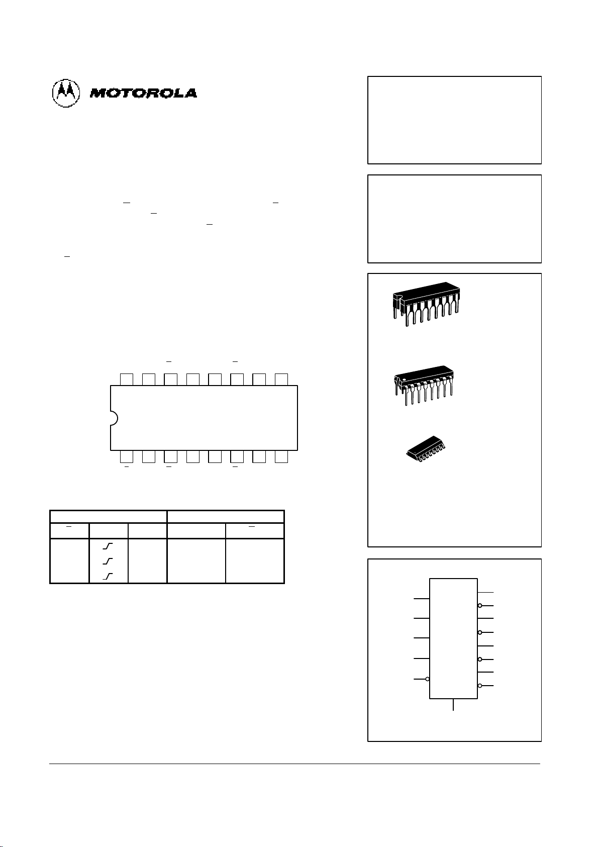
CONNECTION DIAGRAM (TOP VIEW)
1516 14 13 12 11 10
21 3 4 5 6 7
V
CC
9
8
Q3Q
3D3D2Q2Q2
CP
E
Q0Q
0D0D1Q1Q1
GND
FUNCTION TABLE
Inputs Outputs
E CP D
n
Q
n
Q
n
H X NC NC
L H H L
L L L H
H = HIGH Voltage Level
L = LOW Voltage Level
X = Don’t Care
NC = No Change
9
15
14
10
11
7
6
2
3
1
4
5
12
13
D
3
D
2
D
1
D
0
E
Q
3
Q
2
Q
1
Q
0
MC54/74F379
QUAD PARALLEL REGISTER
WITH ENABLE
FAST SCHOTTKY TTL
J SUFFIX
CERAMIC
CASE 620-09
N SUFFIX
PLASTIC
CASE 648-08
16
1
16
1
ORDERING INFORMATION
MC54FXXXJ Ceramic
MC74FXXXN Plastic
MC74FXXXD SOIC
16
1
D SUFFIX
SOIC
CASE 751B-03
LOGIC SYMBOL
VCC = PIN 16
GND = PIN 8
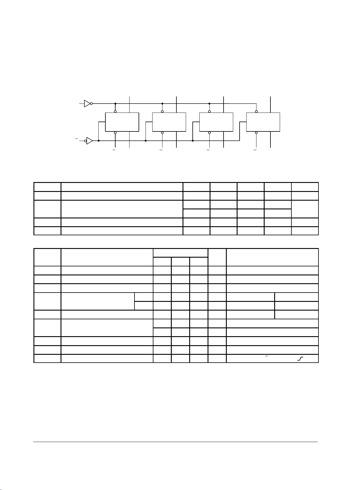
4-177
FAST AND LS TTL DATA
MC54/74F379
D
3
Q
3Q3
E
CP D
Q Q
D
2
Q
2Q2
E
CP D
Q Q
D
1
Q
1
Q
1
E
CP D
Q Q
E
CP
LOGIC DIAGRAM
D
0
Q
0
Q
0
E
CP D
Q Q
GUARANTEED OPERATING RANGES
Symbol Parameter Min Typ Max Unit
V
CC
Supply Voltage 54, 74 4.5 5.0 5.5 V
T
A
Operating Ambient Temperature Range 54 –55 25 125 °C
74 0 25 70
I
OH
Output Current — HIGH 54, 74 –1.0 mA
I
OL
Output Current — LOW 54, 74 20 mA
DC CHARACTERISTICS OVER OPERATING TEMPERATURE RANGE (unless otherwise specified)
Limits
Symbol Parameter Min Typ Max Unit Test Conditions
V
IH
Input HIGH Voltage 2.0 V Guaranteed Input HIGH Voltage
V
IL
Input LOW Voltage 0.8 V Guaranteed Input LOW Voltage
V
IK
Input Clamp Diode Voltage –1.2 V VCC = MIN, IIN = – 18 mA
V
OH
Output HIGH Voltage 54, 74 2.5 V IOL = – 1.0 mA VCC = 4.5 V
74 2.7 V IOL = – 1.0 mA VCC = 4.75 V
V
OL
Output LOW Voltage 0.5 V IOL = 20 mA VCC = MIN
I
IH
Input HIGH Current 20 µA VCC = MAX, VIN = 2.7 V
0.1 mA VCC = MAX, VIN = 7.0 V
I
IL
Input LOW Current –0.6 mA VCC = MAX, VIN = 0.5 V
I
OS
Output Short Circuit Current (Note 2) –60 –150 mA VCC = MAX, V
OUT
= 0 V
I
CC
Power Supply Current 28 40 mA VCC = MAX, D = E = GND, CP =
NOTES:
1. For conditions shown as MIN or MAX, use the appropriate value specified under recommended operating conditions for the applicable device type.
2. Not more than one output should be shorted at a time, nor for more than 1 second.
 Loading...