

Motorola MC74F378N, MC74F378D Datasheet
4-173
FAST AND LS TTL DATA
PARALLEL D REGISTER
WITH ENABLE
The MC54/74F378 is a 6-bit register with a buffered common enable. This
device is similar to the F174 but with common Enable rather than common
Master Reset.
The F378 consists of six edge-triggered D-type flip-flops with individual D
inputs and Q outputs. The Clock (CP) and Enable (E
) inputs are common to
all flip-flops.
When the E input is LOW, new data is entered into the register on the LOW to-HIGH transition of the CP input. When the E
input is HIGH the register will
retain the present data independent of the CP input. This circuit is designed
to prevent false clocking by transitions on the E input..
• 6-Bit High-Speed Parallel Register
• Positive Edge-Triggered D-Type Inputs
• Fully Buffered Common Clock and Enable Inputs
• Input Clamp Diodes Limit High-Speed Termination Effects
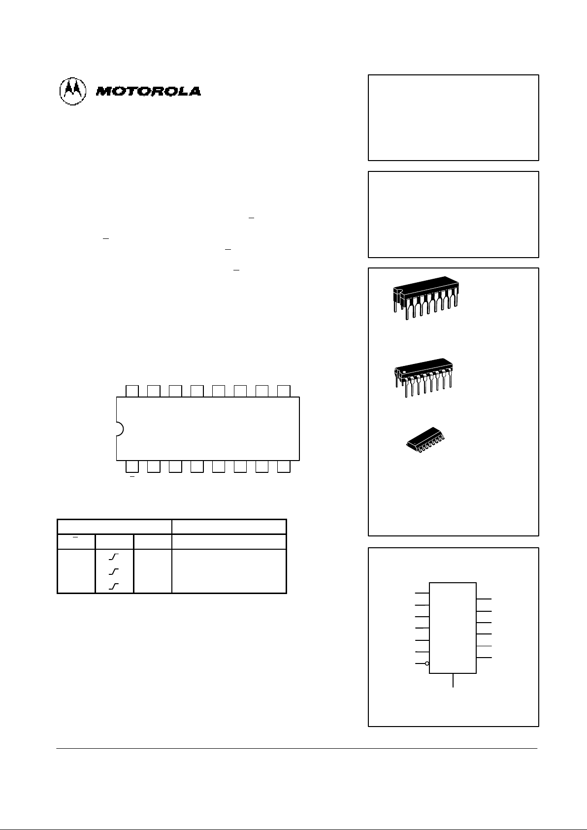
CONNECTION DIAGRAM (TOP VIEW)
1516 14 13 12 11 10
21 3 4 5 6 7
V
CC
9
8
Q5D5D4Q4D3Q3CP
E
Q0D0D1Q1D2Q2GND
FUNCTION TABLE
Inputs Output
E CP D
n
Q
n
H X No Change
L H H
L L L
H = HIGH Voltage Level
L = LOW Voltage Level
X = Don’t Care
Z = High Impedance
MC54/74F378
PARALLEL D REGISTER
WITH ENABLE
FAST SCHOTTKY TTL
J SUFFIX
CERAMIC
CASE 620-09
N SUFFIX
PLASTIC
CASE 648-08
16
1
16
1
ORDERING INFORMATION
MC54FXXXJ Ceramic
MC74FXXXN Plastic
MC74FXXXD SOIC
16
1
D SUFFIX
SOIC
CASE 751B-03
LOGIC SYMBOL
VCC = PIN 16
GND = PIN 8
14
13
12
11
10
9
7
6
5
4
3
2
15
D
5
D
3
D
2
D
1
D
0
D
4
Q
5
Q
3
Q
2
Q
1
Q
0
Q
4
CP
1
E

4-174
FAST AND LS TTL DATA
MC54/74F378
D
5
Q
5
CP D
E
Q
D
4
Q
4
CP D
E
Q
D
3
Q
3
CP D
E
Q
D
2
Q
2
CP D
E
Q
D
1
Q
1
CP D
E
Q
LOGIC DIAGRAM
D
0
Q
0
CP
E
CP D
E
Q
GUARANTEED OPERATING RANGES
Symbol Parameter Min Typ Max Unit
V
CC
Supply Voltage 54, 74 4.5 5.0 5.5 V
T
A
Operating Ambient Temperature Range 54 –55 25 125 °C
74 0 25 70
I
OH
Output Current — HIGH 54, 74 –1.0 mA
I
OL
Output Current — LOW 54, 74 20 mA
DC CHARACTERISTICS OVER OPERATING TEMPERATURE RANGE (unless otherwise specified)
Limits
Symbol Parameter Min Typ Max Unit Test Conditions
V
IH
Input HIGH Voltage 2.0 V Guaranteed Input HIGH Voltage
V
IL
Input LOW Voltage 0.8 V Guaranteed Input LOW Voltage
V
IK
Input Clamp Diode Voltage –1.2 V VCC = MIN, IIN = –18 mA
V
OH
Output HIGH Voltage 54, 74 2.5 V IOL = – 1.0 mA VCC = 4.50 V
74 2.7 V IOL = – 1.0 mA VCC = 4.75 V
V
OL
Output LOW Voltage 0.5 V IOL = 20 mA VCC = MIN
I
IH
Input HIGH Current 20 µA VCC = MAX, VIN = 2.7 V
0.1 mA VCC = MAX, VIN = 7.0 V
I
IL
Input LOW Current –0.6 mA VCC = MAX, VIN = 0.5 V
I
OS
Output Short Circuit Current (Note 2) – 60 –150 mA VCC = MAX, V
OUT
= 0 V
I
CC
Power Supply Current 30 45 mA VCC = MAX, VCP = 0 V
NOTES:
1. For conditions shown as MIN or MAX, use the appropriate value specified under recommended operating conditions for the applicable device type.
2. Not more than one output should be shorted at a time, nor for more than 1 second.
 Loading...