

4-278
FAST AND LS TTL DATA
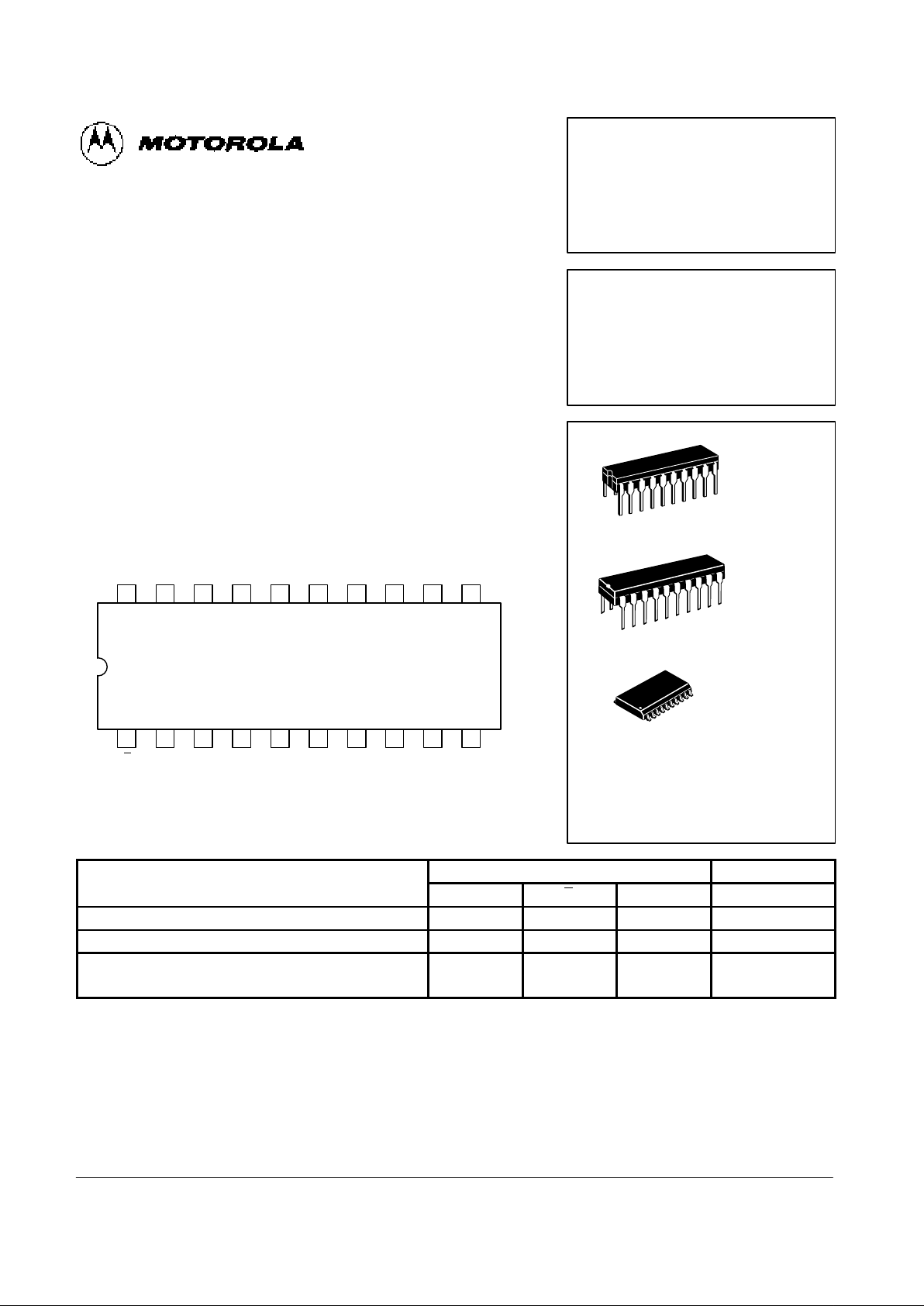
OCTAL D FLIP-FLOP WITH ENABLE
The MC74F377 is a high-speed 8-Bit Register. The register consists of
eight D-Type Flip-Flops with individual D inputs and Q outputs. The common
buffered clock (CP) input loads all flip-flops simultaneously when the Enable
(E) is LOW. This device is supplied in a 20-pin package.
• High Impedance NPN Base Inputs for Reduced Loading (20 µA in
HIGH and LOW States)
• Ideal for Addressable Register Applications
• Enable for Address and Data Synchronization Applications
• Eight Edge-Triggered D Flip-Flops
• Buffered Common Clock
• See: MC74F373 for Transparent Latch Version
MC74F374 for 3-State Version
20 14
2 3 4 5 6 7 8 9 10
D
0
E
Q
0
D1Q
1
D
2
Q
2
D
3
GNDQ
3
11121315171819 16
V
CCQ7D7D6
Q
6
D
5
Q
5
D
4
CPQ
4
1
CONNECTION DIAGRAM (TOP VIEW)
FUNCTION TABLE
Inputs Outputs
Operating Mode CP E D
n
Q
n
Load “1” ↑ l h H
Load “0” ↑ l l L
Hold (do nothing) ↑ h X No Change
X H X No Change
H = HIGH voltage level steady state; h = HIGH voltage level one setup time prior to the LOW-to-HIGH Clock transition; L = LOW voltage level steady state; l =
LOW voltage level one setup time prior to the LOW-to-HIGH clock transition; X = Don’t Care; ↑ = LOW-to-HIGH clock transition
DW SUFFIX
SOIC
CASE 751D-03
20
1
N SUFFIX
PLASTIC
CASE 738-03
20
1
J SUFFIX
CERAMIC
CASE 732-03
20
1
MC74F377
OCTAL D FLIP-FLOP
WITH ENABLE
ORDERING INFORMATION
MC74FXXXJ Ceramic
MC74FXXXN Plastic
MC74FXXXDW SOIC
FAST SCHOTTKY TTL
4-279
FAST AND LS TTL DATA
MC74F377
FUNCTIONAL DESCRIPTION
The MC74F377 has eight edge-triggered D-type flip-flops
with individual D inputs and Q outputs. The common buffered
Clock (CP) input loads all flip-flops simultaneously, when the
Enable (E
) is LOW.
The register is fully edge-triggered. The state of each D input, one setup time before the LOW-to-HIGH clock transition,
is transferred to the corresponding flip-flop’s Q output.
The E input must be stable one setup time prior to the LOWto-HIGH clock transition for predictable operation.
GUARANTEED OPERATING RANGES
Symbol Parameter Min Typ Max Unit
V
CC
Supply Voltage 74 4.5 5.0 5.5 V
T
A
Operating Ambient Temperature Range 74 0 25 70 °C
I
OH
Output Current — HIGH 74 –1.0 mA
I
OL
Output Current — LOW 74 20 mA
DC CHARACTERISTICS OVER OPERATING TEMPERATURE RANGE (unless otherwise specified)
Limits
Symbol Parameter Min Typ Max Unit Test Conditions
V
IH
Input HIGH Voltage 2.0 V Guaranteed Input HIGH Voltage
V
IL
Input LOW Voltage 0.8 V Guaranteed Input LOW Voltage
V
IK
Input Clamp Diode Voltage –1.2 V IIN = –18 mA VCC = MIN
V
OH
Output HIGH Voltage 2.5 2.5 V IOH = –1.0 mA VCC = 4.5 V
2.7 2.7 VCC = 4.75 V
V
OL
Output LOW Voltage 0.35 0.5 V IOL = 20 mA VCC = MIN
I
IH
Input HIGH Current 20 µA VIN = 2.7 V VCC = MAX
I
IL
Input LOW Current –20 µA VIN = 0.5 V VCC = MAX
I
OS
Output Short Circuit Current (Note 2) –60 –150 mA V
OUT
= 0 V VCC = MAX
I
CC
Total Supply Current I
CCH
55 72 mA Dn = 4.5 V, CP = ↑,
E
= GND
VCC = MAX
I
CCL
70 90 mA Dn = E = GND, CP = ↑
NOTES:
1. For conditions shown as MIN or MAX, use the appropriate value specified under recommended operating conditions for the applicable device type.
2. Not more than one output should be shorted at a time, nor for more than 1 second.
AC ELECTRICAL CHARACTERISTICS
74F 74F
TA = +25°C TA = 0 to +70°C
VCC = +5.0 V VCC = 5.0 V ± 10%
CL = 50 pF CL = 50 pF
Symbol Parameter Min Typ Max Min Max Unit
f
MAX
Maximum Clock Frequency 110 120 100 MHz
t
PLH
Propagation Delay 4.0 6.5 8.5 4.0 10 ns
t
PHL
CP to Q
n
4.0 7.0 9.0 4.0 10.5
 Loading...