

4-170
FAST AND LS TTL DATA
OCTAL D-TYPE FLIP-FLOP
WITH 3-STATE OUTPUTS
The MC54/74F374 is a high-speed, low-power octal D-type flip-flop featuring separate D-type inputs for each flip-flop and 3-state outputs for bus oriented applications. A buffered Clock (CP) and Output Enable (OE) are common to all flip-flops.
• Edge-triggered D-Type Inputs
• Buffered Positive Edge-triggered Clock
• 3-State Outputs for Bus-Oriented Applications
• ESD
>
4000 Volts
20 14
2 3 4 5 6 7 8 9 10
D
0
OE
O
0
D1O
1
D
2
O
2
D
3
GNDO
3
11121315171819 16
V
CCO7D7D6
O
6
D
5
O
5
D
4
CPO
4
1
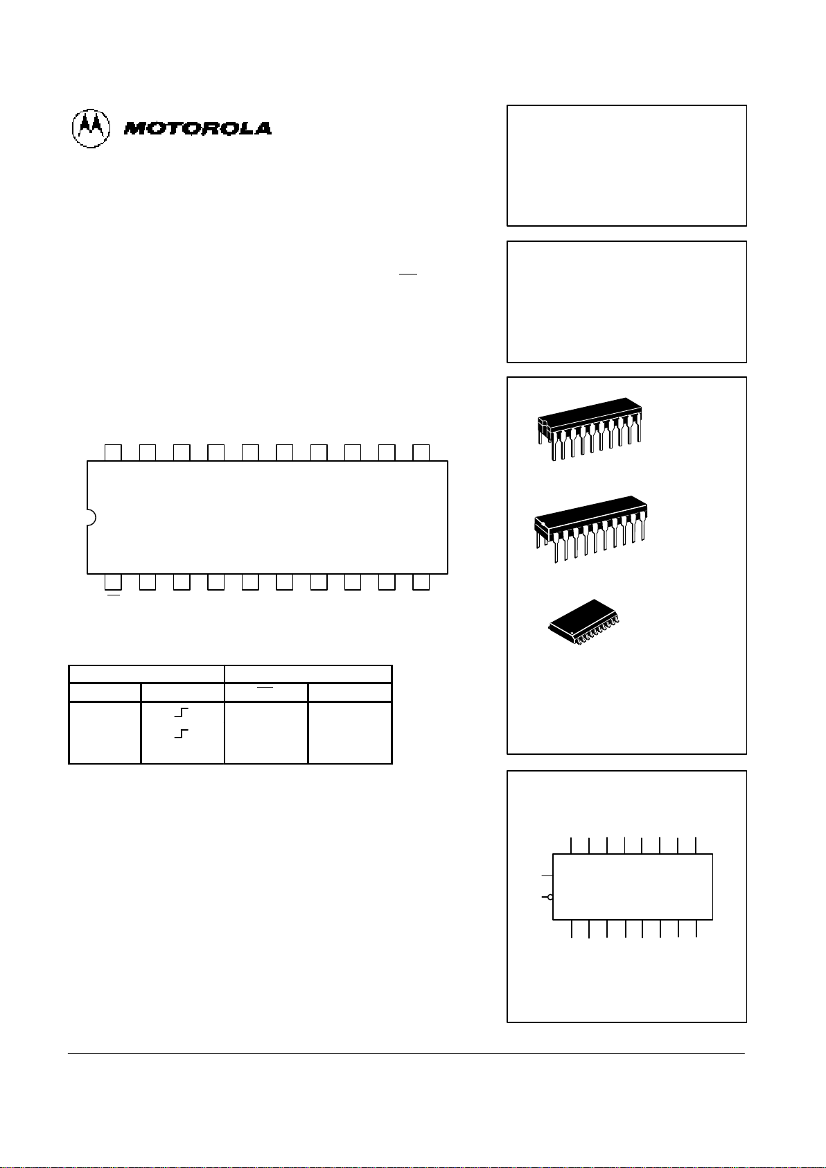
CONNECTION DIAGRAM (TOP VIEW)
FUNCTION TABLE
Inputs Outputs
D
n
CP OE O
n
H L H
L L L
X X H Z
H = HIGH Voltage Level
L = LOW Voltage Level
X = Don’t Care
Z = High Impedance
DW SUFFIX
SOIC
CASE 751D-03
20
1
N SUFFIX
PLASTIC
CASE 738-03
20
1
J SUFFIX
CERAMIC
CASE 732-03
20
1
MC54/74F374
OCTAL D-TYPE FLIP-FLOP
WITH 3-STATE OUTPUTS
FAST SCHOTTKY TTL
ORDERING INFORMATION
MC54FXXXJ Ceramic
MC74FXXXN Plastic
MC74FXXXDW SOIC
LOGIC SYMBOL
VCC = PIN 20
GND = PIN 10
3 4 7 8 13 14 17 18
11
1
2 5 6 9 12 15 16 19
D0 D1 D2 D3 D4 D5 D6 D
7
CP
OE
O0 O1 O2 O3 O4 O5 O6 O
7
4-171
FAST AND LS TTL DATA
MC54/74F374
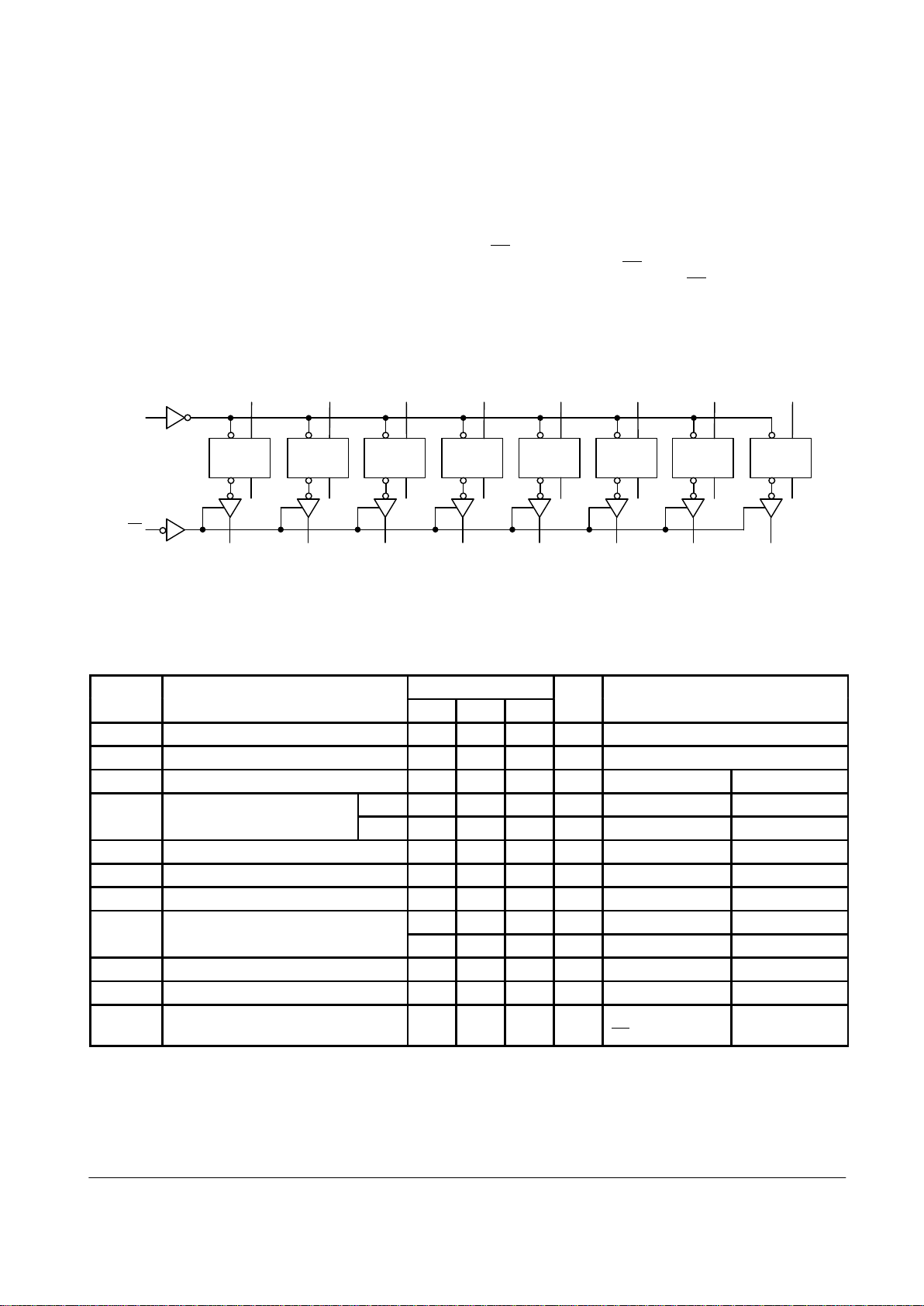
FUNCTIONAL DESCRIPTION
The F374 consists of eight edge-triggered flip-flops with
individual D-type inputs and 3-state true outputs. The buffered
clock and buffered Output Enable are common to all flip-flops.
The eight flip-flops will store the state of their individual D
inputs that meet the setup and hold time requirements on the
LOW-to-HIGH Clock (CP) transition. With the Output Enable
(OE
) LOW, the contents of the eight flip-flops are available at
the outputs. When the OE
is HIGH, the outputs go to the high
impedance state. Operation of the OE
input does not affect the
state of the flip-flops.
O
7
D
7
CP D
Q Q
O
6
D
6
CP D
Q Q
O
5
D
5
CP D
Q Q
O
4
D
4
CP D
Q Q
O
3
D
3
CP D
Q Q
O
2
D
2
CP D
Q Q
O
1
D
1
CP D
Q Q
O
0
OE
CP
LOGIC DIAGRAM
D
0
CP D
Q Q
DC CHARACTERISTICS OVER OPERATING TEMPERATURE RANGE (unless otherwise specified)
Limits
Symbol Parameter Min Typ Max Unit Test Conditions
V
IH
Input HIGH Voltage 2.0 V Guaranteed Input HIGH Voltage
V
IL
Input LOW Voltage 0.8 V Guaranteed Input LOW Voltage
V
IK
Input Clamp Diode Voltage –1.2 V IIN = –18 mA VCC = MIN
V
OH
Output HIGH Voltage 54, 74 2.4 3.3 V IOH = – 3.0 mA VCC = 4.5 V
74 2.7 3.3 V IOH = – 3.0 mA VCC = 4.75 V
V
OL
Output LOW Voltage 0.35 0.5 V IOL = 24 mA VCC = MIN
I
OZH
Output OFF Current — HIGH 50 µA V
OUT
= 2.7 V VCC = MAX
I
OZL
Output OFF Current — LOW –50 µA V
OUT
= 0.5 V VCC = MAX
I
IH
Input HIGH Current 20 µA VIN = 2.7 V VCC = MAX
100 µA VIN = 7.0 V VCC = MAX
I
IL
Input LOW Current –0.6 mA VIN = 0.5 V VCC = MAX
I
OS
Output Short Circuit Current (Note 2) –60 –150 mA V
OUT
= 0 V VCC = MAX
I
CCZ
Power Supply Current (All Outputs OFF) 55 86 mA Dn, = GND
OE
= 4.5 V
VCC = MAX
NOTES:
1. For conditions shown as MIN or MAX, use the appropriate value specified under recommended operating conditions for the applicable device type.
2. Not more than one output should be shorted at a time, nor for more than 1 second.
 Loading...