

Motorola MC74F373DW, MC54F373J, MC74F373N Datasheet
4-167
FAST AND LS TTL DATA
OCTAL TRANSPARENT LATCH
WITH 3-STATE OUTPUTS
The MC54/74F373 consists of eight latches with 3-state outputs for bus organized system applications. The flip-flops appear transparent to the data
when Latch Enable (LE) is HIGH. When LE is LOW, the data that meets the
setup times is latched. Data appears on the bus when the Output Enable (OE
)
is LOW. When OE
is HIGH the bus output is in the high impedance state.
• Eight Latches in a Single Package
• 3-State Outputs for Bus Interfacing
• ESD
>
4000 Volts
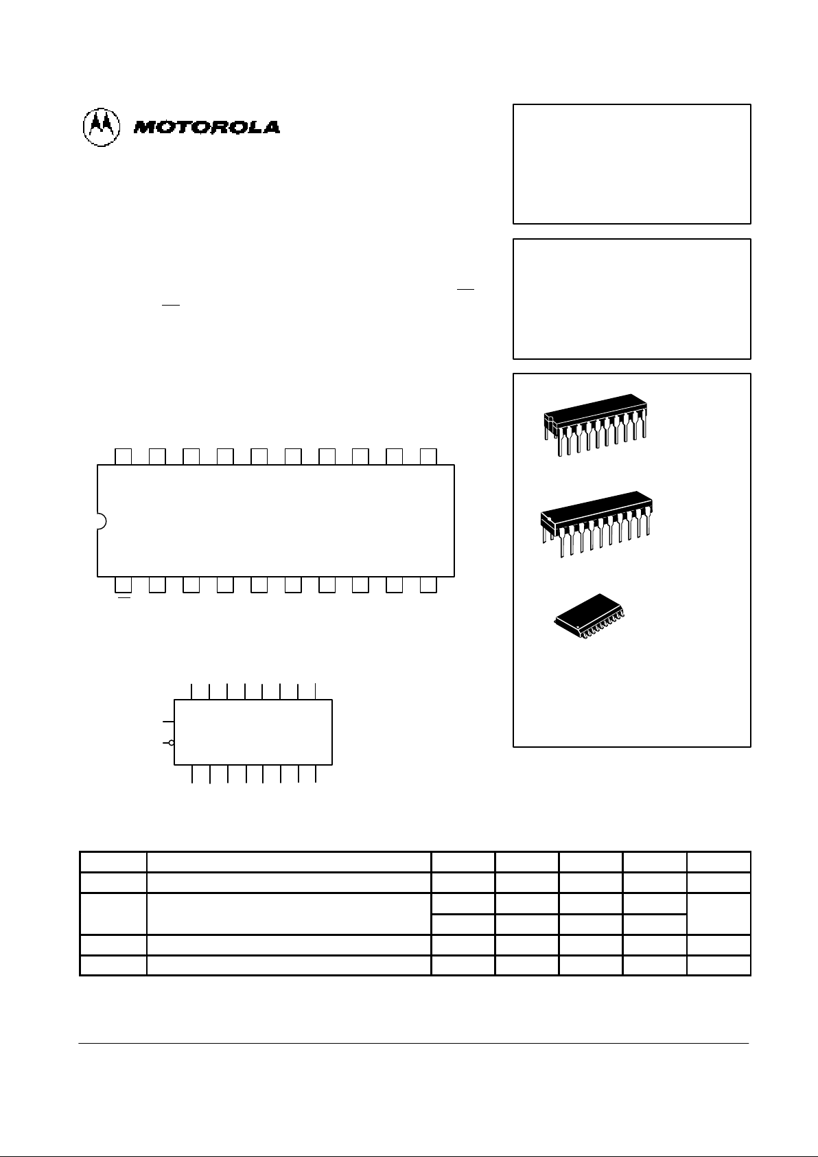
20 14
2 3 4 5 6 7 8 9 10
D
0
OE
O
0
D1O
1
D
2
O
2
D
3
GNDO
3
11121315171819 16
V
CCO7D7D6
O
6
D
5
O
5
D
4
LEO
4
1
CONNECTION DIAGRAM (TOP VIEW)
LOGIC SYMBOL
VCC = PIN 20
GND = PIN 10
3 4 7 8 13 14 17 18
11
1
2 5 6 9 12 15 16 19
D0 D1 D2 D3 D4 D5 D6 D
7
LE
OE
O0 O1 O2 O3 O4 O5 O6 O
7
GUARANTEED OPERATING RANGES
Symbol Parameter Min Typ Max Unit
V
CC
Supply Voltage 54, 74 4.5 5.0 5.5 V
T
A
Operating Ambient Temperature Range 54 –55 25 125 °C
74 0 25 70
I
OH
Output Current — HIGH 54, 74 –3.0 mA
I
OL
Output Current — LOW 54, 74 24 mA
DW SUFFIX
SOIC
CASE 751D-03
20
1
N SUFFIX
PLASTIC
CASE 738-03
20
1
J SUFFIX
CERAMIC
CASE 732-03
20
1
MC54/74F373
OCTAL TRANSPARENT LATCH
WITH 3-STATE OUTPUTS
FAST SCHOTTKY TTL
ORDERING INFORMATION
MC54FXXXJ Ceramic
MC74FXXXN Plastic
MC74FXXXDW SOIC
4-168
FAST AND LS TTL DATA
MC54/74F373
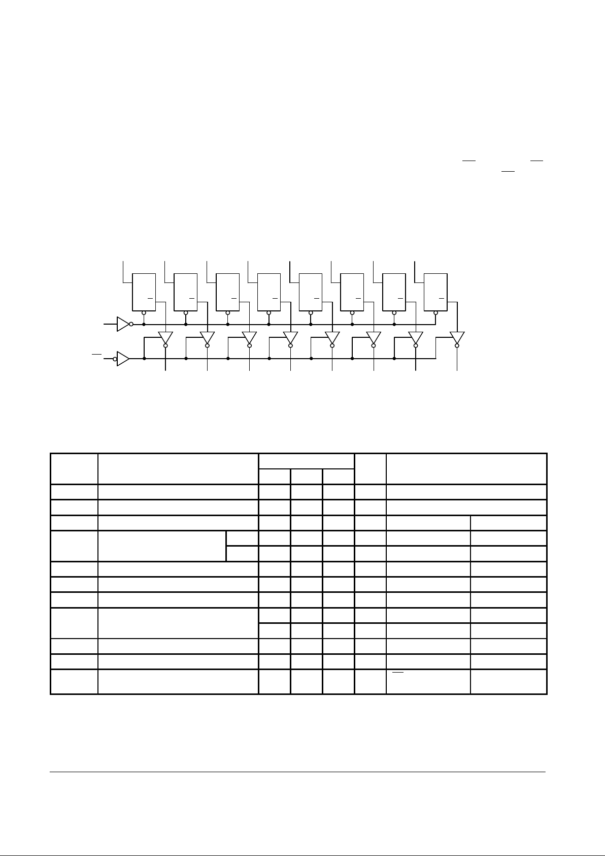
FUNCTIONAL DESCRIPTION
The F373 contains eight D-type latches with 3-state output
buffers. When the Latch Enable (LE) input is HIGH, data on the
Dn inputs enters the latches. In this condition the latches are
transparent; i.e., a latch output will change state each time its
D input changes. When LE is LOW the latches store the
information that was present on the D inputs one setup time
preceding the HIGH-to-LOW transition of LE. The 3-state buffers are controlled by the Output Enable (OE
) input. When (OE)
is LOW, the buffers are in the bi-state mode. When OE
is HIGH
the buffers are in the high impedance mode, but this does not
interfere with entering new data into the latches.
D
7
O
7
D
G
O
D
6
O
6
D
G
O
D
5
O
5
D
G
O
D
4
O
4
D
G
O
D
3
O
3
D
G
O
D
2
O
2
D
G
O
D
1
O
1
D
G
O
LOGIC DIAGRAM
NOTE:
This diagram is provided only for the understanding of logic
operations and should not be used to estimate propagation delays.
LE
OE
D
0
O
0
D
G
O
DC CHARACTERISTICS OVER OPERATING TEMPERATURE RANGE (unless otherwise specified)
Limits
Symbol Parameter Min Typ Max Unit Test Conditions
V
IH
Input HIGH Voltage 2.0 V Guaranteed Input HIGH Voltage
V
IL
Input LOW Voltage 0.8 V Guaranteed Input LOW Voltage
V
IK
Input Clamp Diode Voltage –1.2 V IIN = –18 mA VCC = MIN
V
OH
Output HIGH Voltage 54, 74 2.4 3.3 V IOH = – 3.0 mA VCC = 4.5 V
74 2.7 3.3 V IOH = – 3.0 mA VCC = 4.75 V
V
OL
Output LOW Voltage 0.35 0.5 V IOL = 24 mA VCC = MIN
I
OZH
Output OFF Current — HIGH 50 µA V
OUT
= 2.7 V VCC = MAX
I
OZL
Output OFF Current — LOW –50 µA V
OUT
= 0.5 V VCC = MAX
I
IH
Input HIGH Current 20 µA VIN = 2.7 V VCC = MAX
100 µA VIN = 7.0 V VCC = MAX
I
IL
Input LOW Current –0.6 mA VIN = 0.5 V VCC = MAX
I
OS
Output Short Circuit Current (Note 2) –60 –150 mA V
OUT
= 0 V VCC = MAX
I
CCZ
Power Supply Current (All Outputs OFF) 35 55 mA OE = 4.5 V
Dn, LE = GND
VCC = MAX
NOTES:
1. For conditions shown as MIN or MAX, use the appropriate value specified under recommended operating conditions for the applicable device type.
2. Not more than one output should be shorted at a time, nor for more than 1 second.
 Loading...