

Motorola MC74F256N, MC54F256J, MC74F256D Datasheet
4-123
FAST AND LS TTL DATA
DUAL 4-BIT
ADDRESSABLE LATCH
The MC54/74F256 dual addressable latch has four distinct modes of operation which are selectable by controlling the Clear and Enable inputs (see
Function Table). In the addressable latch mode, data at the Data (D) inputs
is written into the addressed latches. The addressed latches will follow the
Data input with all unaddressed latches remaining in their previous states.
In the memory mode, all latches remain in their previous states and are unaffected by the Data or Address inputs. T o eliminate the possibility of entering
erroneous data in the latches, the enable should be held HIGH (inactive) while
the address lines are changing. In the dual 1-of-4 decoding or demultiplexing
mode (MR
= E = LOW), addressed outputs will follow the level of the D inputs
with all other outputs LOW. In the clear mode, all outputs are LOW and uneffected by the Address and Data inputs.
• Combines Dual Demultiplexer and 8-Bit Latch
• Serial-to-Parallel Capability
• Output from Each Storage Bit Available
• Random (Addressable) Data Entry
• Easily Expandable
• Common Clear Input
• Useful as Dual 1-of-4 Active HIGH Decoder
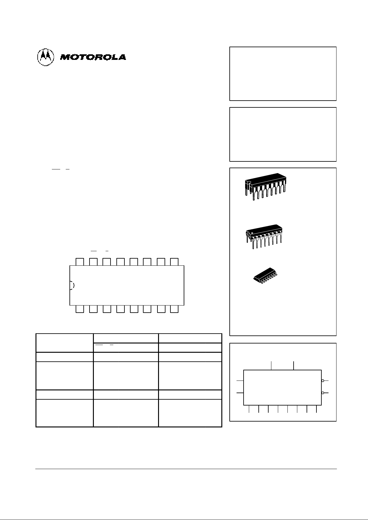
14 13 12 11 10 9
1 2 3 4 5 6
7
16 15
8
V
CC
A
0
MR
E DbQ
3b
Q
1b
Q
2b
Q
0b
A1DaQ0aQ1aQ2aQ3aGND
CONNECTION DIAGRAM
FUNCTION TABLE
Inputs Outputs
Operating Mode MR E D A0A1Q0Q1Q2Q
3
Master Reset L H X X X L L L L
L L d L L Q=d L L L
Demultiplex (Active
L L d H L L Q=d L L
HIGH Decoder when
L L d L H L L Q=d L
D = H)
L L d H H L L L Q=d
Store (Do Nothing) H H X X X q
0
q
1
q
2
q
3
H L d L L Q=d q
1
q
2
q
3
Addressable
H L d H L q0Q=d q
2
q
3
Latch
H L d L H q
0
q1Q=d q
3
H L d H H q
0
q
1
q2Q=d
H = HIGH Voltage Level Steady State
L = LOW Voltage Level Steady State
X = Immaterial
d = HIGH or LOW Data one setup time prior to the LOW-to-HIGH Enable transition.
q = Lower case letters indicate the state of the referenced output established during the last cycle
in which it was addressed or cleared.
MC54/74F256
DUAL 4-BIT
ADDRESSABLE LATCH
J SUFFIX
CERAMIC
CASE 620-09
N SUFFIX
PLASTIC
CASE 648-08
16
1
16
1
ORDERING INFORMATION
MC54FXXXJ Ceramic
MC74FXXXN Plastic
MC74FXXXD SOIC
16
1
D SUFFIX
SOIC
CASE 751B-03
LOGIC SYMBOL
D
a
D
b
E
MR
A
0
A
1
Q0aQ1aQ2aQ3aQ0bQ1bQ2bQ
3b
FAST SCHOTTKY TTL
3 13
1
2
14
15
4 5 6 7 9 10 11 12
4-124
FAST AND LS TTL DATA
MC54/74F256
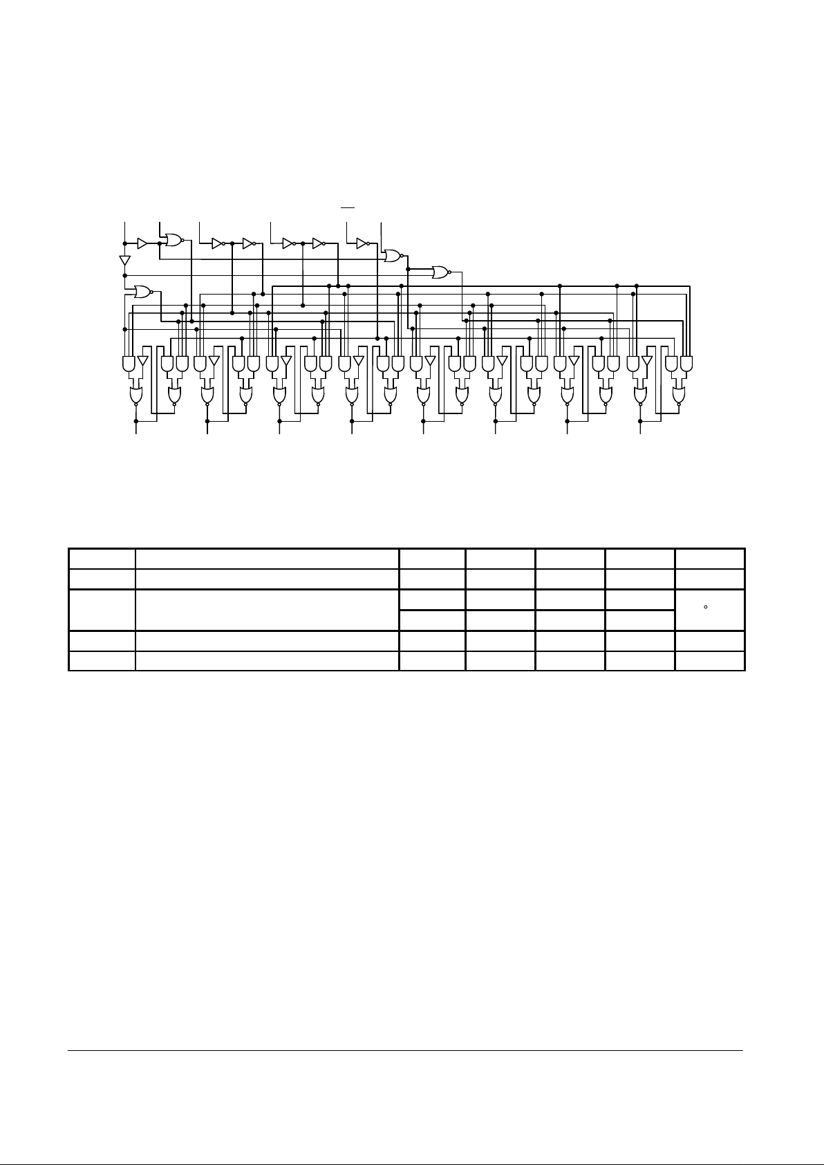
LOGIC DIAGRAM
Please note that this diagram is provided only for the understanding of logic operations and should not be used to estimate propagation delays.
E D
a
A
0
A
1
MR D
b
Q
0a
Q
1a
Q
2a
Q
3a
Q
0b
Q
1b
Q
2b
Q
3b
GUARANTEED OPERATING RANGES
Symbol Parameter Min Typ Max Unit
V
CC
Supply Voltage 54, 74 4.5 5.0 5.5 V
54 –55 25 125
TAOperating Ambient Temperature Range
74 0 25 70
°C
I
OH
Output Current — High 54, 74 –1.0 mA
I
OL
Output Current — Low 54, 74 20 mA
 Loading...