

Motorola MC74F253D, MC74F253N, MC54F253J Datasheet
4-120
FAST AND LS TTL DATA
DUAL 4-INPUT MULTIPLEXER
WITH 3-STATE OUTPUTS
The MC54/74F253 is a Dual 4-Input Multiplexer with 3-State Outputs. It can
select two bits of data from four sources using common select inputs. The outputs may be individually switched to a high-impedance state with a HIGH on
the respective Output Enable (OE
) inputs, allowing the outputs to interface di-
rectly with bus-oriented systems.
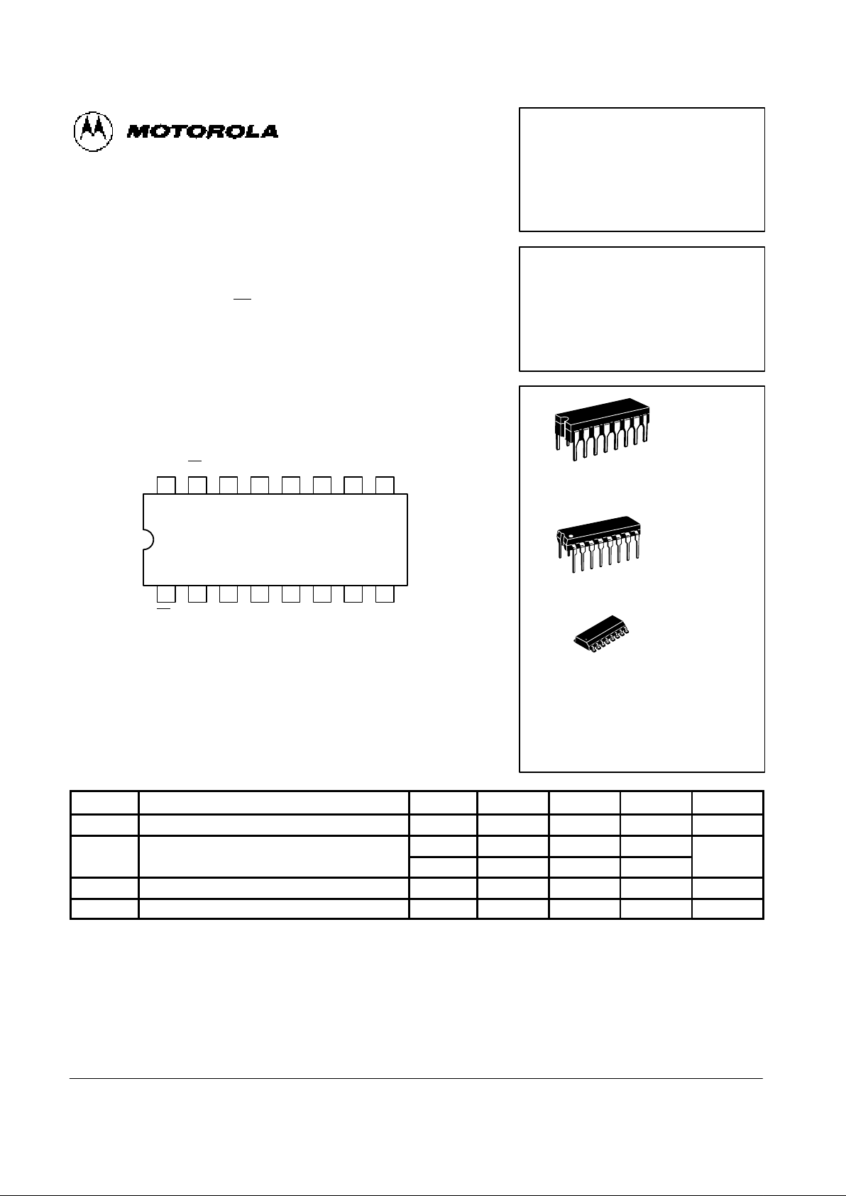
1516 14 13 12 11 10
21 3 4 5 6 7
V
CC
9
8
OE
b
GND
S0I
3bI2bI1bI0bZb
OE
aS1I3aI2aI1aI0aZa
CONNECTION DIAGRAM DIP (TOP VIEW)
GUARANTEED OPERATING RANGES
Symbol Parameter Min Typ Max Unit
V
CC
Supply Voltage 54, 74 4.5 5.0 5.5 V
T
A
Operating Ambient Temperature Range 54 –55 25 125 °C
74 0 25 70
I
OH
Output Current — High 54, 74 –3.0 mA
I
OL
Output Current — Low 54, 74 24 mA
FAST SCHOTTKY TTL
DUAL 4-INPUT MULTIPLEXER
WITH 3-STATE OUTPUTS
MC54/74F253
J SUFFIX
CERAMIC
CASE 620-09
N SUFFIX
PLASTIC
CASE 648-08
16
1
16
1
ORDERING INFORMATION
MC54FXXXJ Ceramic
MC74FXXXN Plastic
MC74FXXXD SOIC
16
1
D SUFFIX
SOIC
CASE 751B-03
H = HIGH Voltage Level
L = LOW Voltage Level
X = Don’t Care
Z = High Impedance (off)
Address inputs S0 and S1
are common to both sections.
4-121
FAST AND LS TTL DATA
MC54/74F253
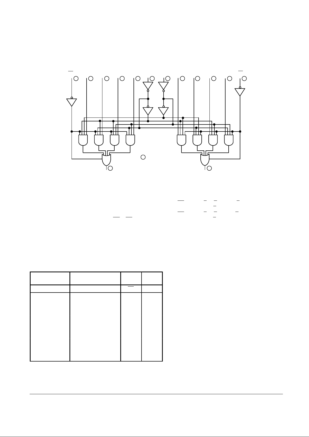
9 7
16210 1411
LOGIC DIAGRAM
OE
b
1
3b
1
2b
1
1b
1
0b
S
0
S
1
1
3a
1
2a
1
1a
1
0a
OE
a
Z
a
Z
b
VCC = PIN 16
GND = PIN 8
= PIN NUMBERS
3 4 5121315
FUNCTIONAL DESCRIPTION
The F253 contains two identical 4-input Multiplexers with
3-State Outputs. They select two bits from four sources selected by common Select Inputs (S0, S1). The 4-input multiplexers have individual Output Enable (OE
a
, OEb) inputs
which, when HIGH, force the outputs to a high impedance
(high Z) state.
The F253 is the logic implementation of a 2-pole, 4-position
switch, where the position of the switch is determined by the
logic levels supplied to the two select inputs. The logic equations for the outputs are shown below:
Za = OE
a
• (I0a • S1 • S0 + I1a • S1 • S0 +
I2a • S1 • S
0
+ 13a • S1 • S0)
Zb = OE
b
• (I0b • S1 • S0 + I1b • S1 • S0 +
I2b • S1 • S
0
+ I3b • S1 • S0)
If the outputs of 3-state devices are tied together, all but one
device must be in the high impedance state to avoid high currents that would exceed the maximum ratings. Designers
should ensure that Output Enable signals to 3-state devices
whose outputs are tied together are designed so that there is
no overlap.
FUNCTION TABLE
Select
Inputs
Data Inputs
Output
Enable
Output
S
0
S
1
I
0
I
1
I
2
I
3
OE Z
X X X X X X H Z
L L L X X X L L
L L H X X X L H
H L X L X X L L
H L X H X X L H
L H X X L X L L
L H X X H X L H
H H X X X L L L
H H X X X H L H
 Loading...