

Motorola MC74ACT374N, MC74AC374N, MC74AC374DW Datasheet
5-1
FACT DATA
The MC74AC374/74ACT374 is a high-speed, low-power octal D-type flip-flop
featuring separate D-type inputs for each flip-flop and 3-state outputs for busoriented applications. A buffered Clock (CP) and Output Enable (OE
) are common
to all flip-flops.
• Buffered Positive Edge-Triggered Clock
• 3-State Outputs for Bus-Oriented Applications
• Outputs Source/Sink 24 mA
• See MC74AC273 for Reset Version
• See MC74AC377 for Clock Enable Version
• See MC74AC373 for Transparent Latch Version
• See MC74AC574 for Broadside Pinout Version
• See MC74AC564 for Broadside Pinout Version with Inverted Outputs
• ′ACT374 Has TTL Compatible Inputs
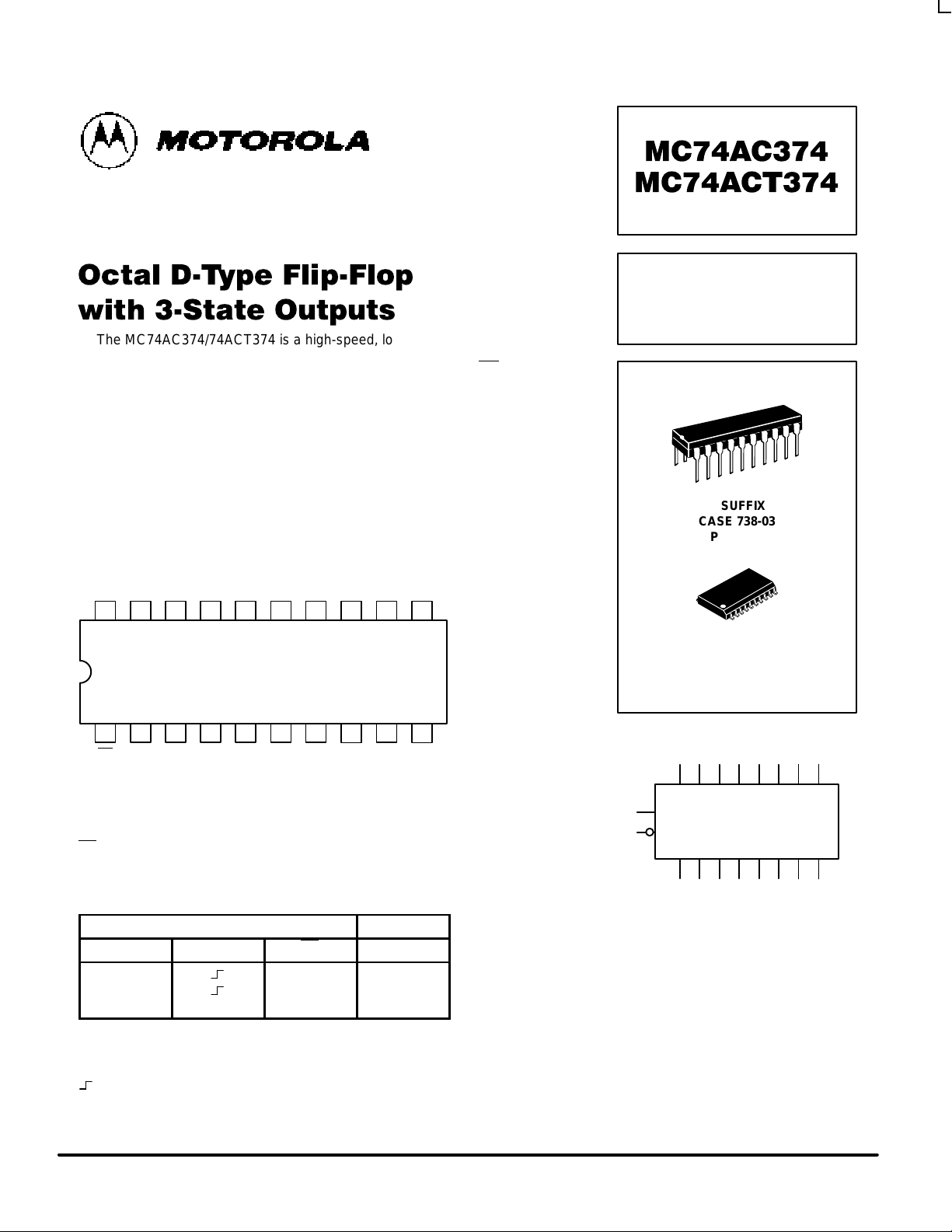
1920 18 17 16 15 14
21 3 4 5 6 7
V
CC
13
8
12
9
11
10
O7D7D6O6O5D5D4O4CP
OE
O0D0D1O1O2D2D3O3GND
PIN NAMES
D0–D7 Data Inputs
CP Clock Pulse Input
OE
3-State Output Enable Input
O0–O73-State Outputs
TRUTH TABLE
Inputs Outputs
D
n
CP OE O
n
H L H
L L L
X X H Z
H = HIGH Voltage Level
L = LOW Voltage Level
X = Immaterial
Z = High Impedance
= LOW-to-HIGH Transition
OCTAL D-TYPE
FLIP-FLOP WITH
3-STATE OUTPUTS
N SUFFIX
CASE 738-03
PLASTIC
DW SUFFIX
CASE 751D-04
PLASTIC
LOGIC SYMBOL
O0O1O2O3O4O5O6O
7
D0D1D2D3D4D5D6D
7
CP
OE
MC74AC374 MC74ACT374
5-2
FACT DATA
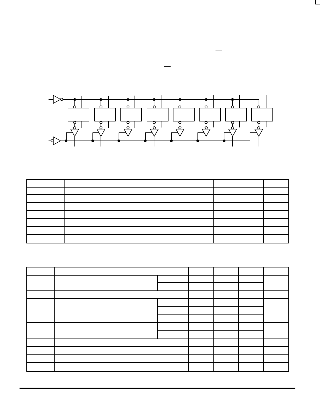
FUNCTIONAL DESCRIPTION
The MC74AC374/74ACT374 consists of eight edgetriggered flip-flops with individual D-type inputs and 3-state
true outputs. The buffered clock and buffered Output Enable
are common to all flip-flops. The eight flip-flops will store the
state of their individual D inputs that meet the setup and hold
time requirements on the LOW-to-HIGH Clock (CP) transition.
With the Output Enable (OE
) LOW, the contents of the eight
flip-flops are available at the outputs. When the OE
is HIGH,
the outputs go to the high impedance state. Operation of the
OE
input does not affect the state of the flip-flops.
CP D
Q Q
CP D
Q Q
CP D
Q Q
CP D
Q Q
CP D
Q Q
CP D
Q Q
CP D
Q Q
CP D
Q Q
LOGIC DIAGRAM
D
0
D
1
D
2
D
3
D
4
D
5
D
6
D
7
O
0
O
1
O
2
O
3
O
4
O
5
O
6
O
7
OE
CP
Please note that this diagram is provided only for the understanding of logic
operations and should not be used to estimate propagation delays.
MAXIMUM RATINGS*
Symbol Parameter Value Unit
V
CC
DC Supply Voltage (Referenced to GND) –0.5 to +7.0 V
V
in
DC Input Voltage (Referenced to GND) –0.5 to VCC +0.5 V
V
out
DC Output Voltage (Referenced to GND) –0.5 to VCC +0.5 V
I
in
DC Input Current, per Pin ±20 mA
I
out
DC Output Sink/Source Current, per Pin ±50 mA
I
CC
DC VCC or GND Current per Output Pin ±50 mA
T
stg
Storage Temperature –65 to +150 °C
* Maximum Ratings are those values beyond which damage to the device may occur. Functional operation should be restricted to the Recommended
Operating Conditions.
RECOMMENDED OPERATING CONDITIONS
Symbol Parameter Min Typ Max Unit
′AC 2.0 5.0 6.0
VCCSupply Voltage
′ACT 4.5 5.0 5.5
V
Vin, V
out
DC Input Voltage, Output Voltage (Ref. to GND) 0 V
CC
V
VCC @ 3.0 V 150
Input Rise and Fall Time (Note 1)
′AC Devices except Schmitt Inputs
VCC @ 4.5 V 40 ns/V
r
, t
f
′AC Devices except Schmitt Inputs
VCC @ 5.5 V 25
VCC @ 4.5 V 10
tr, t
f
Input Rise and Fall Time (Note 2)
′ACT Devices except Schmitt Inputs
VCC @ 5.5 V 8.0
ns/V
T
J
Junction Temperature (PDIP) 140 °C
T
A
Operating Ambient Temperature Range –40 25 85 °C
I
OH
Output Current — High –24 mA
I
OL
Output Current — Low 24 mA
1. Vin from 30% to 70% VCC; see individual Data Sheets for devices that differ from the typical input rise and fall times.
2. Vin from 0.8 V to 2.0 V; see individual Data Sheets for devices that differ from the typical input rise and fall times.
tr, t
f
Input Rise and Fall Time (Note 2)
MC74AC374 MC74ACT374
5-3
FACT DATA
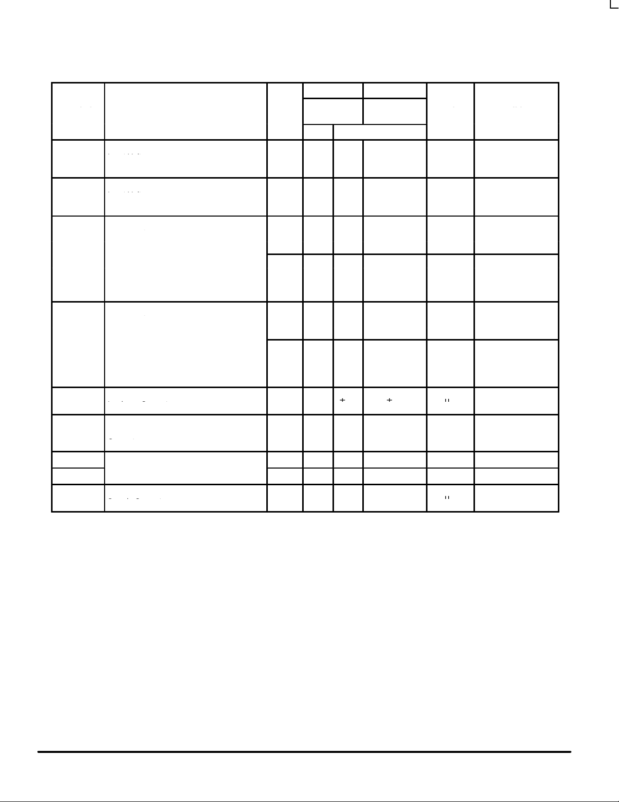
DC CHARACTERISTICS
74AC 74AC
Symbol
Parameter
V
CC
(V)
TA = +25°C
TA =
–40°C to +85°C
Unit
Conditions
Typ Guaranteed Limits
V
IH
3.0 1.5 2.1 2.1 V
OUT
= 0.1 V
4.5 2.25 3.15 3.15 V or VCC – 0.1 V
5.5 2.75 3.85 3.85
V
IL
3.0 1.5 0.9 0.9 V
OUT
= 0.1 V
4.5 2.25 1.35 1.35 V or VCC – 0.1 V
5.5 2.75 1.65 1.65
V
OH
3.0 2.99 2.9 2.9 I
OUT
= –50 µA
4.5 4.49 4.4 4.4 V
5.5 5.49 5.4 5.4
*VIN = VIL or V
IH
3.0 2.56 2.46
–12 mA
4.5 3.86 3.76
V
I
OH
–24 mA
5.5 4.86 4.76 –24 mA
V
OL
3.0 0.002 0.1 0.1 I
OUT
= 50 µA
4.5 0.001 0.1 0.1 V
5.5 0.001 0.1 0.1
*VIN = VIL or V
IH
3.0 0.36 0.44
12 mA
4.5 0.36 0.44
V
I
OL
24 mA
5.5 0.36 0.44 24 mA
I
IN
5.5
±0.1
±1.0
µA
VI = VCC, GND
I
OZ
VI (OE) = VIL, V
IH
5.5 ±0.5 ±5.0 µA VI = VCC, GND
VO = VCC, GND
I
OLD
5.5 75 mA V
OLD
= 1.65 V Max
I
OHD
Output Current
5.5 –75 mA V
OHD
= 3.85 V Min
I
CC
5.5
8.080µA
VIN = VCC or GND
* All outputs loaded; thresholds on input associated with output under test.
†Maximum test duration 2.0 ms, one output loaded at a time.
Note: IIN and ICC @ 3.0 V are guaranteed to be less than or equal to the respective limit @ 5.5 V VCC.
Minimum High Level
Input Voltage
Maximum Low Level
Input Voltage
Minimum High Level
Output Voltage
Maximum Low Level
Output Voltage
Maximum Input
Leakage Current
Maximum
3-State
Current
†Minimum Dynamic
Maximum Quiescent
Supply Current
 Loading...