

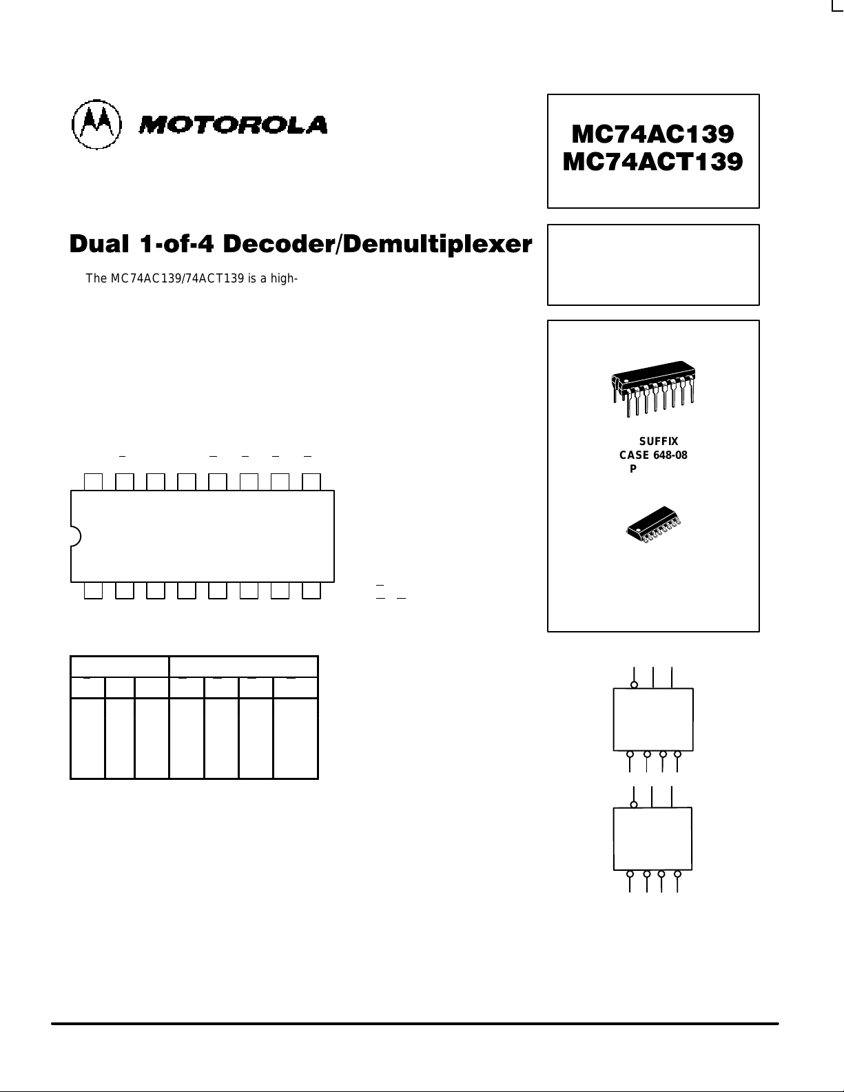
Motorola MC74ACT139N, MC74ACT139D, MC74AC139D Datasheet
5-1
FACT DATA
The MC74AC139/74ACT139 is a high-speed, dual 1-of-4 decoder/demultiplexer.
The device has two independent decoders, each accepting two inputs and providing
four mutually-exclusive active-LOW outputs. Each decoder has an active-LOW
Enable input which can be used as a data input for a 4-output demultiplexer. Each
half of the MC74AC139/74ACT139 can be used as a function generator providing
four minterms of two variables.
• Multifunction Capability
• Two Completely Independent 1-of-4 Decoders
• Active LOW Mutually Exclusive Outputs
• Outputs Source/Sink 24 mA
• ′ACT139 Has TTL Compatible Inputs
1516 14 13 12 11 10
21 3 4 5 6 7
V
CC
9
8
E
bA0bA1b
E
a
GND
O
0bO1bO2bO3b
A0aA1aO
0aO1aO2aO3a
PIN NAMES
A0, A1Address Inputs
E
Enable Inputs
O
0–O3
Outputs
TRUTH TABLE
Inputs Outputs
E A0A1O0O1O
2
O
3
H X X H H H H
L L L L H H H
L H L H L H H
L L H H H L H
L H H H H H L
H = HIGH Voltage Level
L = LOW Voltage Level
X = Immaterial
DUAL 1-OF-4
DECODER/DEMULTIPLEXER
N SUFFIX
CASE 648-08
PLASTIC
D SUFFIX
CASE 751B-05
PLASTIC
E A0A
1
O0O1O2O
3
DECODER a
LOGIC SYMBOL
E
A0A
1
O0O1O2O
3
DECODER b
MC74AC139 MC74ACT139
5-2
FACT DATA
E
a
A0aA
1a
E
b
A0bA
1b
0
0a
0
1a
0
2a
0
3a
0
0b
0
1b
0
2b
0
3b
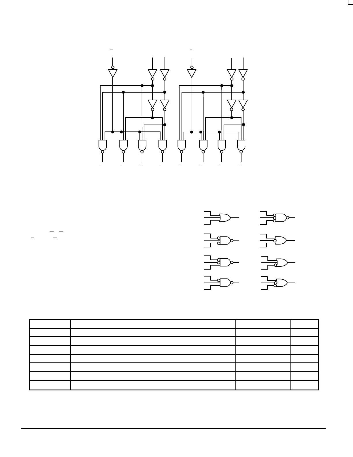
Please note that this diagram is provided only for the understanding of logic
operations and should not be used to estimate propagation delays.
LOGIC DIAGRAM
FUNCTIONAL DESCRIPTION
The MC74AC139/74ACT139 is a high-speed dual 1-of-4
decoder/demultiplexer. The device has two independent
decoders, each of which accepts two binary weighted inputs
(A0–A1) and provides four mutually exclusive active-LOW
outputs (O
0–O3
). Each decoder has an active-LOW enable
(E
). When E is HIGH all outputs are forced HIGH. The enable
can be used as the data input for a 4-output demultiplexer
application. Each half of the MC74AC139/74ACT139
generates all four minterms of two variables. These four
minterms are useful in some applications, replacing multiple
gate functions as shown in Figure a, and thereby reducing the
number of packages required in a logic network.
E
A
0
A
1
E
A
0
A
1
E
A
0
A
1
E
A
0
A
1
E
A
0
A
1
E
A
0
A
1
E
A
0
A
1
E
A
0
A
1
O
0
O
0
O
1
O
1
O
2
O
2
O
3
O
3
Figure a: Gate Functions (each half)
MAXIMUM RATINGS*
Symbol Parameter Value Unit
V
CC
DC Supply Voltage (Referenced to GND) –0.5 to +7.0 V
V
in
DC Input Voltage (Referenced to GND) –0.5 to VCC +0.5 V
V
out
DC Output Voltage (Referenced to GND) –0.5 to VCC +0.5 V
I
in
DC Input Current, per Pin ±20 mA
I
out
DC Output Sink/Source Current, per Pin ±50 mA
I
CC
DC VCC or GND Current per Output Pin ±50 mA
T
stg
Storage Temperature –65 to +150 °C
* Maximum Ratings are those values beyond which damage to the device may occur. Functional operation should be restricted to the Recommended
Operating Conditions.
 Loading...