

Motorola MC74AC05N, MC74AC05D Datasheet
5-1
FACT DATA
The MC74AC/ACT05 is identical in pinout to the LS05. The device inputs are
compatible with standard CMOS outputs; with pullup resistors, they are compatible
with TTL outputs.
• Outputs Source/Sink 24 mA
• ′ACT05 Has TTL Compatible Inputs
GND
Pinout: 14-Lead Packages (Top View)
1314 12 11 10 9 8
21 3 4 5 6 7
V
CCA6Y6A5Y5A4Y4
A1Y1A2Y2A3Y
3
FUNCTION TABLE
Input A Output Y
L
H
Z
L
MAXIMUM RATINGS*
Symbol Parameter Value Unit
V
CC
DC Supply Voltage (Referenced to GND) –0.5 to +7.0 V
V
in
DC Input Voltage (Referenced to GND) –0.5 to VCC + 0.5 V
V
out
DC Output Voltage (Referenced to GND) –0.5 to VCC + 0.5 V
I
in
DC Input Current, per Pin ± 20 mA
I
out
DC Output Sink/Source Current, per Pin ± 50 mA
I
CC
DC VCC or GND Current per Output Pin ± 50 mA
T
stg
Storage Temperature –65 to +150 °C
* Maximum Ratings are those values beyond which damage to the device may occur. Functional operation should be restricted to the Recommended
Operating Conditions.
HEX INVERTER WITH
OPEN-DRAIN OUTPUTS
N SUFFIX
CASE 646-06
PLASTIC PACKAGE
D SUFFIX
CASE 751A-03
PLASTIC PACKAGE
Z = High Impedance
MC74AC05 MC74ACT05
5-2
FACT DATA
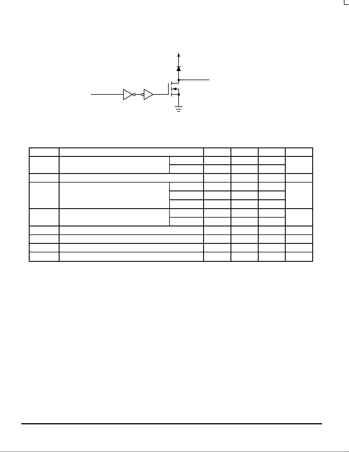
LOGIC DIAGRAM
Y*
2, 4, 6, 8, 10, 12
1, 3, 5, 9, 11, 13
A
PIN 14 = VCC
PIN 7 = GND
* DENOTES OPEN-DRAIN OUTPUTS
RECOMMENDED OPERATING CONDITIONS
Symbol Parameter Min Typ Min Unit
′AC 2.0 5.0 6.0
VCCSupply Voltage
′ACT 4.5 5.0 5.5
V
VREG DC Regulated Power Voltage (Ref. to GND) 0 V
CC
V
VCC @ 3.0 V 150
Input Rise and Fall Time (Note 1)
′AC Devices except Schmitt Inputs
VCC @ 4.5 V 40 ns/V
r
, t
f
′AC Devices except Schmitt Inputs
VCC @ 5.5 V 25
VCC @ 4.5 V 10
tr, t
f
Input Rise and Fall Time (Note 2)
′ACT Devices except Schmitt Inputs
VCC @ 5.5 V 8.0
ns/V
T
J
Junction Temperature (PDIP) 140 °C
T
A
Operating Ambient Temperature Range –40 25 85 °C
I
OH
Output Current — HIGH –24 mA
I
OL
Output Current — LOW 24 mA
1. Vin from 30% to 70% VCC; see individual Data Sheets for devices that differ from the typical input rise and fall times.
2. Vin from 0.8 V to 2.0 V; see individual Data Sheets for devices that differ from the typical input rise and fall times.
tr, t
f
Input Rise and Fall Time (Note 2)
 Loading...