

Motorola MC68341FT25, MC68341FT16, MC68341FT16V Datasheet

Parts Not Suitable for New Designs
For Additional Information
End-Of-Life Product Change Notice
MC68341
Integrated Processor
User’s Manual
Motorola reserves the right to make changes without further notice to any products herein. Motorola makes no warranty, representation or guarantee regarding
the suitability of its products for any particular purpose, nor does Motorola assume any liability arising out of the application or use of any product or circuit, and
specifically disclaims any and all liability, including without limitation consequential or incidental damages. "Typical" parameters can and do vary in different
applications. All operating parameters, including "Typicals" must be validated for each customer application by customer's technical experts. Motorola does not
convey any license under its patent rights nor the rights of others. Motorola products are not designed, intended, or authorized for use as components in systems
intended for surgical implant into the body, or other applications intended to support or sustain life, or for any other application in which the failure of the Motorola
product could create a situation where personal injury or death may occur. Should Buyer purchase or use Motorola products for any such unintended or
unauthorized application, Buyer shall indemnify and hold Motorola and its officers, employees, subsidiaries, affiliates, and distributors harmless against all claims,
costs, damages, and expenses, and reasonable attorney fees arising out of, directly or indirectly, any claim of personal injury or death associated with such
unintended or unauthorized use, even if such claim alleges that Motorola was negligent regarding the design or manufacture of the part. Motorola and are
registered trademarks of Motorola, Inc. Motorola, Inc. is an Equal Opportunity/Affirmative Action Employer.
µ
© MOTOROLA, 1993

PREFACE
The complete documentation package for the MC68341 consists of the MC68341UM/AD,
MC68341 Integrated Processor User’s Manual
Programmer’s Reference Manual,
Product Brief
.
and the MC68341P/D,
, M68000PM/AD,
MC68341 Integrated Processor
MC68000 Family
The
capabilities, registers, and operation of the MC68341; the
Reference Manual
Integrated Processor Product Brief
capabilities.
This user’s manual is organized as follows:
MC68341 Integrated Processor User’s Manual
provides instruction details for the MC68341; and the
provides a brief description of the MC68341
Section 1 Device Overview Section 9 Queued Serial Peripheral
Section 2 Signal Descriptions Module
Section 3 Bus Operation Section 10 IEEE 1149.1 Test Access
Section 4 System Integration Module Port
Section 5 CPU32 Section 11 Applications
Section 6 DMA Controller Module Section 12 Electrical Characteristics
Section 7 Serial Module Section 13 Ordering Information and
Section 8 Timer Modules Mechanical Data
68K FAX-IT –
Documentation Comments
describes the programming,
MC68000 Family Programmer’s
MC68341
FAX 512-891-8593—Documentation Comments Only
The Motorola High-End Technical Publications Department provides a fax number for you
to submit any questions or comments about this document or how to order other
documents. We welcome your suggestions for improving our documentation. Please do
not fax technical questions.
Please provide the part number and revision number (located in upper right-hand corner
of the cover) and the title of the document. When referring to items in the manual, please
reference by the page number, paragraph number, figure number, table number, and line
number if needed.
When sending a fax, please provide your name, company, fax number, and phone
number including area code.
Applications and Technical Information
For questions or comments pertaining to technical information, questions, and
applications, please contact one of the following sales offices nearest you.

— Sales Offices —
UNITED STATES
ALABAMA, Huntsville (205) 464-6800
ARIZONA, Tempe (602) 897-5056
CALIFORNIA, Agoura Hills (818) 706-1929
CALIFORNIA, Los Angeles (310) 417-8848
CALIFORNIA, Irvine (714) 753-7360
CALIFORNIA, Rosevllle (916) 922-7152
CALIFORNIA, San Diego (619) 541-2163
CALIFORNIA, Sunnyvale (408) 749-0510
COLORADO, Colorado Springs (719) 599-7497
COLORADO, Denver (303) 337-3434
CONNECTICUT, Wallingford (203) 949-4100
FLORIDA, Maitland (407) 628-2636
FLORIDA, Pompano Beach/Fort.
Lauderdale (305) 486-9776
FLORIDA, Clearwater (813) 538-7750
GEORGlA, Atlanta (404) 729-7100
IDAHO, Boise (208) 323-9413
ILLINOIS, Chicago/Hoffman Estates (708) 490-9500
INDlANA, Fort Wayne (219) 436-5818
INDIANA, Indianapolis (317) 571-0400
INDIANA, Kokomo (317) 457-6634
IOWA, Cedar Rapids (319) 373-1328
KANSAS, Kansas City/Mission (913) 451-8555
MARYLAND, Columbia (410) 381-1570
MASSACHUSETTS, Marborough (508) 481-8100
MASSACHUSETTS, Woburn (617) 932-9700
MICHIGAN, Detroit (313) 347-6800
MINNESOTA, Minnetonka (612) 932-1500
MISSOURI, St. Louis (314) 275-7380
NEW JERSEY, Fairfield (201) 808-2400
NEW YORK, Fairport (716) 425-4000
NEW YORK, Hauppauge (516) 361-7000
NEW YORK, Poughkeepsie/Fishkill (914) 473-8102
NORTH CAROLINA, Raleigh (919) 870-4355
OHIO, Cleveland (216) 349-3100
OHIO, Columbus Worthington (614) 431-8492
OHIO, Dayton (513) 495-6800
OKLAHOMA, Tulsa (800) 544-9496
OREGON, Portland (503) 641-3681
PENNSYLVANIA, Colmar (215) 997-1020
Philadelphia/Horsham (215) 957-4100
TENNESSEE, Knoxville (615) 690-5593
TEXAS, Austin (512) 873-2000
TEXAS, Houston (800) 343-2692
TEXAS, Plano (214) 516-5100
VIRGINIA, Richmond (804) 285-2100
WASHINGTON, Bellevue (206) 454-4160
Seattle Access (206) 622-9960
WISCONSIN, Milwaukee/Brookfield (414) 792-0122
Field Applications Engineering Available
Through All Sales Offices
CANADA
BRITISH COLUMBIA, Vancouver (604) 293-7605
ONTARIO, Toronto (416) 497-8181
ONTARIO, Ottawa (613) 226-3491
QUEBEC, Montreal (514) 731-6881
INTERNATIONAL
AUSTRALIA, Melbourne (61-3)887-0711
AUSTRALIA, Sydney (61(2)906-3855
BRAZIL, Sao Paulo 55(11)815-4200
CHINA, Beijing 86 505-2180
FINLAND, Helsinki 358-0-35161191
Car Phone 358(49)211501
FRANCE, Paris/Vanves 33(1)40 955 900
GERMANY, Langenhagen/ Hanover 49(511)789911
GERMANY, Munich 49 89 92103-0
GERMANY, Nuremberg 49 911 64-3044
GERMANY, Sindelfingen 49 7031 69 910
GERMANY,Wiesbaden 49 611 761921
HONG KONG, Kwai Fong 852-4808333
Tai Po 852-6668333
INDIA, Bangalore (91-812)627094
ISRAEL, Tel Aviv 972(3)753-8222
ITALY, Milan 39(2)82201
JAPAN, Aizu 81(241)272231
JAPAN, Atsugi 81(0462)23-0761
JAPAN, Kumagaya 81(0485)26-2600
JAPAN, Kyushu 81(092)771-4212
JAPAN, Mito 81(0292)26-2340
JAPAN, Nagoya 81(052)232-1621
JAPAN, Osaka 81(06)305-1801
JAPAN, Sendai 81(22)268-4333
JAPAN, Tachikawa 81(0425)23-6700
JAPAN, Tokyo 81(03)3440-3311
JAPAN, Yokohama 81(045)472-2751
KOREA, Pusan 82(51)4635-035
KOREA, Seoul 82(2)554-5188
MALAYSIA, Penang 60(4)374514
MEXICO, Mexico City 52(5)282-2864
MEXICO, Guadalajara 52(36)21-8977
Marketing 52(36)21-9023
Customer Service 52(36)669-9160
NETHERLANDS, Best (31)49988 612 11
PUERTO RICO, San Juan (809)793-2170
SINGAPORE (65)2945438
SPAIN, Madrid 34(1)457-8204
or 34(1)457-8254
SWEDEN, Solna 46(8)734-8800
SWITZERLAND, Geneva 41(22)7991111
SWITZERLAND, Zurich 41(1)730 4074
TAlWAN, Taipei 886(2)717-7089
THAILAND, Bangkok (66-2)254-4910
UNITED KINGDOM, Aylesbury 44(296)395-252
FULL LINE REPRESENTATIVES
COLORADO, Grand Junction
Cheryl Lee Whitely (303) 243-9658
KANSAS, Wichita
Melinda Shores/Kelly Greiving (316) 838 0190
NEVADA, Reno
Galena Technology Group (702) 746 0642
NEW MEXICO, Albuquerque
S&S Technologies, lnc. (505) 298-7177
UTAH, Salt Lake City
Utah Component Sales, Inc. (801) 561-5099
WASHINGTON, Spokane
Doug Kenley (509) 924-2322
ARGENTINA, Buenos Aires
Argonics, S.A. (541) 343-1787
HYBRID COMPONENTS RESELLERS
Elmo Semiconductor (818) 768-7400
Minco Technology Labs Inc. (512) 834-2022
Semi Dice Inc. (310) 594-4631

10/31/95 SECTION 1: OVERVIEW UM Rev 1
TABLE OF CONTENTS
Paragraph Page
Number Title Number
Section 1
Device Overview
1.1 Features .............................................................................................. 1-2
Section 2
Signal Descriptions
2.1 Signal Index ........................................................................................ 2-3
2.2 Bus Signals ......................................................................................... 2-5
2.2.1 Address Bus .................................................................................... 2-6
2.2.1.1 Address Bus (A23–A0) ................................................................ 2-6
2.2.1.2 Address Bus (A31–A24) .............................................................. 2-6
2.2.2 Address Strobe (AS)........................................................................ 2-6
2.2.3 M68000 Address Strobe (68KAS) .................................................... 2-6
2.2.4 Data Bus (D15–D0) ......................................................................... 2-6
2.2.5 Data Strobe (DS)............................................................................. 2-7
2.2.6 Upper And Lower Data Strobes (UDS , LDS) ................................... 2-7
2.2.7 Byte Write Enable (UWE , LWE) ....................................................... 2-7
2.2.8 Read/Write (R/W) ............................................................................ 2-7
2.2.9 Transfer Size (SIZ1, SIZ0)............................................................... 2-8
2.2.10 Function Codes (FC3–FC0)............................................................. 2-8
2.2.11 Chip Selects (CS7 –CS1 , CS0 /AVEC).............................................. 2-8
2.2.12 Interrupt Request Level (IRQ7 – IRQ1) ........................................... 2-9
2.3 Bus Control Signals............................................................................. 2-9
2.3.1 Data and Size Acknowledge (DSACK1 , DSACK0) .......................... 2-9
2.4 Bus Arbitration Signals........................................................................ 2-9
2.4.1 Bus Request (BR) ............................................................................ 2-9
2.4.2 Bus Grant (BG )................................................................................ 2-10
2.4.3 Bus Grant Acknowledge (BGACK) .................................................. 2-10
2.4.4 Read-Modify-Write Cycle (RMC/RTCOUT) ..................................... 2-10
2.5 Exception Control Signals ................................................................... 2-10
2.5.1 Reset (RESET) ................................................................................ 2-10
2.5.2 Halt (HALT)...................................................................................... 2-10
2.5.3 Bus Error (BERR )............................................................................ 2-10
2.6 Clock Signals ...................................................................................... 2-11
2.6.1 System Clock (CLKOUT)................................................................. 2-11
2.6.2 Crystal Oscillator (EXTAL, XTAL).................................................... 2-11
MOTOROLA MC68341 USER'S MANUAL iii

10/31/95 SECTION 1: OVERVIEW UM Rev.1.0
TABLE OF CONTENTS (Continued)
Paragraph Page
Number Title Number
2.6.3 External Clock (EXTCLK)................................................................ 2-11
2.6.4 External Filter Capacitor (XFC) ....................................................... 2-11
2.6.5 Clock Mode Select (MODCK, Port B0)............................................ 2-11
2.7 Instrumentation and Emulation Signals............................................... 2-11
2.7.1 Instruction Fetch (IFETCH ).............................................................. 2-11
2.7.2 Instruction Pipe (IPIPE) ................................................................... 2-12
2.7.3 Breakpoint (BKPT ) .......................................................................... 2-12
2.7.4 Freeze (FREEZE)............................................................................ 2-12
2.8 DMA Module Signals .......................................................................... 2-12
2.8.1 DMA Request (DREQ2 , DREQ1 ).................................................... 2-12
2.8.2 DMA Acknowledge (DACK2, DACK1/DDACK2 , DDACK1 ) ............. 2-13
2.8.3 DMA Done (DONE2 , DONE1 )......................................................... 2-13
2.8.4 Data Transfer Complete (DTC ) ....................................................... 2-13
2.8.5 DMA Ready (RDY2, RDY1) ............................................................ 2-13
2.9 Serial Module Signals ......................................................................... 2-13
2.9.1 Serial Crystal Oscillator (X2, X1) ..................................................... 2-13
2.9.2 Serial External Clock Input (SCLK) ................................................. 2-13
2.9.3 Receive Data (RxDA, RxDB)........................................................... 2-14
2.9.4 Transmit Data (TxDA, TxDB)........................................................... 2-14
2.9.5 Clear to Send (CTSA, CTSB) .......................................................... 2-14
2.9.6 Request to Send (RTSA, RTSB) ..................................................... 2-14
2.9.7 Transmitter Ready (T≈RDYA ).......................................................... 2-14
2.9.8 Receiver Ready (R≈RDYA) ............................................................. 2-14
2.10 Queued Serial Module Signals ........................................................... 2-15
2.10.1 Master In Slave Out (MISO)............................................................ 2-15
2.10.2 Master Out Slave In (MOSI)............................................................ 2-15
2.10.3 QSPI Serial Clock (QSCLK)............................................................ 2-15
2.10.4 QSPI Peripheral Chip Select (PCS1, PCS0)................................... 2-15
2.11 Timer Signals ...................................................................................... 2-15
2.11.1 Timer Gate (TGATE2 ) ..................................................................... 2-15
2.11.2 Timer Input (TIN) ............................................................................. 2-16
2.11.3 Timer Output (TOUT) ...................................................................... 2-16
2.12 Test Signals ........................................................................................ 2-16
2.12.1 Test Clock (TCK) ............................................................................. 2-16
2.12.2 Test Mode Select (TMS) ................................................................. 2-16
2.12.3 Test Data In (TDI)............................................................................ 2-16
2.12.4 Test Data Out (TDO) ....................................................................... 2-16
2.13 Real Time Clock Mode Signals........................................................... 2-16
2.13.1 Battery Switch (BSW )...................................................................... 2-16
2.13.2 Battery Voltage (V
2.13.3 Real Time Clock Output (RMC/RTCOUT) ....................................... 2-17
2.14 System Power and Ground (VCC AND GND) .................................... 2-17
BATT
)................................................................. 2-16
iv MC68341 USER’S MANUAL MOTOROLA

10/31/95 SECTION 1: OVERVIEW UM Rev 1
TABLE OF CONTENTS (Continued)
Paragraph Page
Number Title Number
Section 3
Bus Operation
3.1 68000 Bus Mode ..................................................................................... 3-1
3.2 Bus Transfer Signals............................................................................... 3-2
3.2.1 Bus Control Signals ............................................................................. 3-3
3.2.2 Function Code Signals ............................................................................ 3-4
3.2.3 Address Bus (A31–A0)............................................................................ 3-5
3.2.4 Address Strobe (AS) ............................................................................... 3-5
3.2.5 68000 Address Strobe (AS68K) .............................................................. 3-5
3.2.6 Data Bus (D15–D0)................................................................................. 3-5
3.2.7 Data Strobe (DS)..................................................................................... 3-5
3.2.8 Upper and Lower Data Strobes (UDS and LDS )..................................... 3-6
3.2.9 Upper and Lower Write Enables (UWE and LWE) .................................. 3-6
3.2.10 Data Transfer Complete (DTC)............................................................... 3-6
3.2.11 Bus Cycle Termination Signals ............................................................... 3-6
3.2.11.1 Data Transfer and Size Acknowledge Signals
(DSACK1 and DSACK0). ................................................................. 3-6
3.1.11.2 Bus Error (BERR) ............................................................................. 3-7
3.2.11.3 Autovector (AVEC)........................................................................... 3-7
3.3 Data Transfer Mechanism....................................................................... 3-7
3.3.1 Dynamic Bus Sizing ................................................................................ 3-7
3.3.2 Misaligned Operands .............................................................................. 3-9
3.3.3 Operand Transfer Cases......................................................................... 3-10
3.3.3.1 Byte Operand to 8-Bit Port, Odd or Even (A0 = X) .......................... 3-10
3.3.3.2 Byte Operand to 16-Bit Port, Even (A0 = 0)..................................... 3-10
3.3.3.3 Byte Operand to 16-Bit Port, Odd (A0 = 1) ...................................... 3-11
3.3.3.4 Word Operand to 8-Bit Port, Aligned ............................................... 3-11
3.3.3.5 Word Operand to 16-Bit Port, Aligned ............................................. 3-12
3.3.3.6 Long-word Operand to 8-Bit Port, Aligned. ...................................... 3-12
3.3.3.7 Long-Word Operand to 16-Bit Port, Aligned .................................... 3-14
3.3.4 Bus Operation...................................................................................... 3-16
3.3.5 Synchronous Operation with DSACK≈ ................................................ 3-16
3.3.6 Fast Termination Cycles...................................................................... 3-17
3.4 Data Transfer Cycles........................................................................... 3-18
3.4.1 M68300 Read Cycle................................................................................ 3-18
3.4.2 68000 Read Cycle................................................................................... 3-21
3.4.3 M68300 Write Cycle................................................................................ 3-23
3.4.4 68000 Write Cycle................................................................................... 3-26
3.4.5 Read-Modify-Write Cycle ........................................................................ 3-29
3.5 CPU Space Cycles.................................................................................. 3-31
3.5.1 Breakpoint Acknowledge Cycle............................................................... 3-31
MOTOROLA MC68341 USER'S MANUAL v

10/31/95 SECTION 1: OVERVIEW UM Rev.1.0
TABLE OF CONTENTS (Continued)
Paragraph Page
Number Title Number
3.5.2 LPSTOP Broadcast Cycle....................................................................... 3-32
3.5.3 Module Base Address Register Access.................................................. 3-36
3.5.4 Interrupt Acknowledge Bus Cycles ......................................................... 3-36
3.5.4.1 Interrupt Acknowledge Cycle—Terminated Normally.......................... 3-36
3.5.4.2 Autovector Interrupt Acknowledge Cycle............................................. 3-38
3.5.4.3 Spurious Interrupt Cycle...................................................................... 3-39
3.6 Bus Exception Control Cycles................................................................. 3-41
3.6.1 Bus Errors ............................................................................................... 3-43
3.6.2 Retry Operation....................................................................................... 3-45
3.6.3 Halt Operation......................................................................................... 3-47
3.6.4 Double Bus Fault .................................................................................... 3-48
3.7 Bus Arbitration ........................................................................................ 3-49
3.7.1 Bus Request ........................................................................................... 3-52
3.7.2 Bus Grant................................................................................................ 3-52
3.7.3 Bus Grant Acknowledge ......................................................................... 3-52
3.7.4 Bus Arbitration Control............................................................................ 3-53
3.7.5 Show Cycles ........................................................................................... 3-53
3.8 Reset Operation...................................................................................... 3-55
Section 4
System Integration Module
4.1 Module Overview .................................................................................... 4-1
4.2 Module Operation.................................................................................... 4-2
4.2.1 Module Base Address Register Operation .......................................... 4-2
4.2.2 System Configuration and Protection Operation ................................. 4-3
4.2.2.1 System Configuration ...................................................................... 4-5
4.2.2.2 Internal Bus Monitor......................................................................... 4-6
4.2.2.3 Double Bus Fault Monitor ................................................................ 4-6
4.2.2.4 Spurious Interrupt Monitor ............................................................... 4-6
4.2.2.5 Software Watchdog ......................................................................... 4-6
4.2.2.6 Periodic Interrupt Timer ................................................................... 4-7
4.2.2.6.1 Periodic Timer Period Calculation................................................ 4-8
4.2.2.6.2 Using the Periodic Timer as a Real-Time Clock........................... 4-9
4.2.2.7 Simultaneous Interrupts by Sources in the SIM41........................... 4-9
4.2.3 Clock Synthesizer Operation............................................................... 4-9
4.2.3.1 Phase Comparator and Filter........................................................... 4-12
4.2.3.2 Frequency Divider............................................................................ 4-12
4.2.3.3 Clock Control ................................................................................... 4-15
4.2.4 Chip Select Operation ......................................................................... 4-15
4.2.4.1 Programmable Features .................................................................. 4-15
4.2.4.2 Global Chip Select Operation .......................................................... 4-16
vi MC68341 USER’S MANUAL MOTOROLA

10/31/95 SECTION 1: OVERVIEW UM Rev 1
TABLE OF CONTENTS (Continued)
Paragraph Page
Number Title Number
4.2.5 External Bus Interface Operation ........................................................ 4-17
4.2.5.1 Port A. .............................................................................................. 4-17
4.2.5.2 Port B ............................................................................................... 4-17
4.2.6 Low-Power Stop .................................................................................. 4-18
4.2.7 Freeze.................................................................................................. 4-19
4.3 Programming Model ................................................................................ 4-19
4.3.1 Module Base Address Register (MBAR) ............................................. 4-22
4.3.2 System Configuration and Protection Registers.................................. 4-23
4.3.2.1 Module Configuration Register (MCR)............................................. 4-23
4.3.2.2 Autovector Register (AVR)............................................................... 4-25
4.3.2.3 Reset Status Register (RSR) ........................................................... 4-25
4.3.2.4 Software Interrupt Vector Register (SWIV) ...................................... 4-26
4.3.2.5 System Protection Control Register (SYPCR)................................. 4-26
4.3.2.6 Periodic Interrupt Control Register (PICR)....................................... 4-28
4.3.2.7 Periodic Interrupt Timer Register (PITR) ......................................... 4-28
4.3.2.8 Software Service Register (SWSR) ................................................. 4-29
4.3.3 Clock Synthesizer Control Register (SYNCR)..................................... 4-29
4.3.4 Chip Select Registers .......................................................................... 4-31
4.3.4.1 Base Select Registers ......................................................................... 4-31
4.3.4.2 Address Mask Registers.................................................................. 4-33
4.3.4.3 Bus Select Register.......................................................................... 4-35
4.3.4.4 Map Select Register......................................................................... 4-35
4.3.4.5 Chip Select Registers Programming Example................................. 4-35
4.3.5 External Bus Interface Control............................................................. 4-36
4.3.5.1 Port A Pin Assignment Register 1 (PPARA1) .................................. 4-36
4.3.5.2 Port A Pin Assignment Register 2 (PPARA2) .................................. 4-36
4.3.5.3 Port A Data Direction Register (DDRA). .......................................... 4-37
4.3.5.4 Port A Data Register (PORTA) ........................................................ 4-37
4.3.5.5 Port B Pin Assignment Register (PPARB)....................................... 4-37
4.3.5.6 Port B Data Direction Register (DDRB) ........................................... 4-38
4.3.5.7 Port B Data Register (PORTB, PORTB1)........................................ 4-38
4.3.5.8 Port C Pin Assignment Register (PPARC)....................................... 4-38
4.4 Real Time Clock ...................................................................................... 4-39
4.4.1 Reset ................................................................................................... 4-39
4.4.2 RTC Interrupt Control Register (RICR)................................................ 4-39
4.4.3 RTC Control/Status Register (RCR).................................................... 4-40
4.4.3 RTC Calibration Control Register (RCCR) .......................................... 4-41
4.4.4 RTC Time of Day Registers................................................................. 4-43
4.4.5 RTC Alarm Registers........................................................................... 4-45
4.4.6 RTC Power Up Operation.................................................................... 4-46
4.4.7 RTC Power Down Operation............................................................... 4-46
MOTOROLA MC68341 USER'S MANUAL vii

10/31/95 SECTION 1: OVERVIEW UM Rev.1.0
TABLE OF CONTENTS (Continued)
Paragraph Page
Number Title Number
4.5 MC68340 Initialization Sequence............................................................ 4-46
4.5.1 Startup................................................................................................. 4-47
4.5.2 SIM41 Module Configuration............................................................... 4-47
4.5.3 SIM41 Example Configuration Code ................................................... 4-48
SECTION 5
CPU32
5.1 Overview ............................................................................................. 5-1
5.1.1 Features .......................................................................................... 5-2
5.1.2 Virtual Memory ................................................................................ 5-2
5.1.3 Loop Mode Instruction Execution .................................................... 5-3
5.1.4 Vector Base Register....................................................................... 5-4
5.1.5 Exception Handling.......................................................................... 5-4
5.1.6 Addressing Modes........................................................................... 5-5
5.2 Architecture Summary ........................................................................ 5-5
5.2.1 Programming Model ........................................................................ 5-6
5.2.2 Registers ......................................................................................... 5-7
5.3 Instruction Set ..................................................................................... 5-8
5.3.1 M68000 Family Compatibility .......................................................... 5-10
5.3.1.1 New Instructions .......................................................................... 5-10
5.3.1.1.1 Low-Power Stop (LPSTOP) ..................................................... 5-10
5.3.1.1.2 Table Lookup and Interpolate (TBL)......................................... 5-10
5.3.1.2 Unimplemented Instructions ........................................................ 5-10
5.3.2 Instruction Format and Notation...................................................... 5-10
5.3.3 Instruction Summary ....................................................................... 5-13
5.3.3.1 Condition Code Register.............................................................. 5-18
5.3.3.2 Data Movement Instructions ........................................................ 5-19
5.3.3.3 Integer Arithmetic Operations...................................................... 5-20
5.3.3.4 Logic Instructions......................................................................... 5-22
5.3.3.5 Shift and Rotate Instructions........................................................ 5-22
5.3.3.6 Bit Manipulation Instructions........................................................ 5-23
5.3.3.7 Binary-Coded Decimal (BCD) Instructions................................... 5-24
5.3.3.8 Program Control Instructions ....................................................... 5-24
5.3.3.9 System Control Instructions......................................................... 5-25
5.3.3.10 Condition Tests............................................................................ 5-27
5.3.4 Using the TBL Instructions .............................................................. 5-27
5.3.4.1 Table Example 1 Standard Usage ........................................... 5-28
5.3.4.2 Table Example 2 Compressed Table....................................... 5-29
5.3.4.3 Table Example 3 8-Bit Independent Variable........................... 5-30
5.3.4.4 Table Example 4 Maintaining Precision ................................... 5-32
5.3.4.5 Table Example 5 Surface Interpolations .................................. 5-34
5.3.5 Nested Subroutine Calls.................................................................. 5-34
viii MC68341 USER’S MANUAL MOTOROLA

10/31/95 SECTION 1: OVERVIEW UM Rev 1
TABLE OF CONTENTS (Continued)
Paragraph Page
Number Title Number
5.3.6 Pipeline Synchronization with the NOP Instruction ......................... 5-34
5.4 Processing States ............................................................................... 5-34
5.4.1 State Transitions.............................................................................. 5-35
5.4.2 Privilege Levels ............................................................................... 5-35
5.4.2.1 Supervisor Privilege Level ........................................................... 5-35
5.4.2.2 User Privilege Level ..................................................................... 5-36
5.4.2.3 Changing Privilege Level ............................................................. 5-36
5.5 Exception Processing.......................................................................... 5-36
5.5.1 Exception Vectors............................................................................ 5-37
5.5.1.1 Types of Exceptions..................................................................... 5-38
5.5.1.2 Exception Processing Sequence ................................................. 5-38
5.5.1.3 Exception Stack Frame................................................................ 5-39
5.5.1.4 Multiple Exceptions ...................................................................... 5-39
5.5.2 Processing of Specific Exceptions................................................... 5-41
5.5.2.1 Reset............................................................................................ 5-41
5.5.2.2 Bus Error ...................................................................................... 5-43
5.5.2.3 Address Error ............................................................................... 5-43
5.5.2.4 Instruction Traps .......................................................................... 5-44
5.5.2.5 Software Breakpoints................................................................... 5-44
5.5.2.6 Hardware Breakpoints ................................................................. 5-45
5.5.2.7 Format Error ................................................................................. 5-45
5.5.2.8 Illegal or Unimplemented Instructions.......................................... 5-45
5.5.2.9 Privilege Violations....................................................................... 5-46
5.5.2.10 Tracing ......................................................................................... 5-47
5.5.2.11 Interrupts...................................................................................... 5-48
5.5.2.12 Return from Exception ................................................................. 5-49
5.5.3 Fault Recovery ................................................................................ 5-50
5.5.3.1 Types of Faults ............................................................................ 5-52
5.5.3.1.1 Type I—Released Write Faults................................................. 5-52
5.5.3.1.2 Type II—Prefetch, Operand, RMW, and MOVEP Faults.......... 5-53
5.5.3.1.3 Type III—Faults During MOVEM Operand Transfer ................ 5-54
5.5.3.1.4 Type IV—Faults During Exception Processing......................... 5-54
5.5.3.2 Correcting a Fault......................................................................... 5-55
5.5.3.2.1 Type I—Completing Released Writes via Software ................. 5-55
5.5.3.2.2 Type I—Completing Released Writes via RTE......................... 5-55
5.5.3.2.3 Type II—Correcting Faults via RTE.......................................... 5-56
5.5.3.2.4 Type III—Correcting Faults via Software.................................. 5-56
5.5.3.2.5 Type III—Correcting Faults by Conversion and Restart........... 5-56
5.5.3.2.6 Type III—Correcting Faults via RTE......................................... 5-57
5.5.3.2.7 Type IV—Correcting Faults via Software ................................. 5-57
5.5.4 CPU32 Stack Frames...................................................................... 5-58
5.5.4.1 Four-Word Stack Frame .............................................................. 5-58
MOTOROLA MC68341 USER'S MANUAL ix

10/31/95 SECTION 1: OVERVIEW UM Rev.1.0
TABLE OF CONTENTS (Continued)
Paragraph Page
Number Title Number
5.5.4.2 Six-Word Stack Frame................................................................. 5-58
5.5.4.3 Bus Error Stack Frame ................................................................ 5-58
5.6 Development Support ......................................................................... 5-61
5.6.1 CPU32 Integrated Development Support........................................ 5-61
5.6.1.1 Background Debug Mode (BDM) Overview................................. 5-62
5.6.1.2 Deterministic Opcode Tracking Overview.................................... 5-62
5.6.1.3 On-Chip Hardware Breakpoint Overview..................................... 5-63
5.6.2 Background Debug Mode................................................................ 5-63
5.6.2.1 Enabling BDM.............................................................................. 5-63
5.6.2.2 BDM Sources............................................................................... 5-64
5.6.2.2.1 External BKPT Signal............................................................... 5-64
5.6.2.2.2 BGND Instruction ..................................................................... 5-64
5.6.2.2.3 Double Bus Fault...................................................................... 5-64
5.6.2.3 Entering BDM .............................................................................. 5-64
5.6.2.4 Command Execution.................................................................... 5-65
5.6.2.5 BDM Registers............................................................................. 5-65
5.6.2.5.1 Fault Address Register (FAR) .................................................. 5-65
5.6.2.5.2 Return Program Counter (RPC) ............................................... 5-65
5.6.2.5.3 Current Instruction Program Counter (PCC). ........................... 5-65
5.6.2.6 Returning from BDM .................................................................... 5-66
5.6.2.7 Serial Interface............................................................................. 5-66
5.6.2.7.1 CPU Serial Logic...................................................................... 5-67
5.6.2.7.2 Development System Serial Logic ........................................... 5-69
5.6.2.8 Command Set .............................................................................. 5-71
5.6.2.8.1 Command Format .................................................................... 5-71
5.6.2.8.2 Command Sequence Diagram................................................. 5-72
5.6.2.8.3 Command Set Summary.......................................................... 5-73
5.6.2.8.4 Read A/D Register (RAREG/RDREG) ..................................... 5-74
5.6.2.8.5 Write A/D Register (WAREG/WDREG).................................... 5-75
5.6.2.8.6 Read System Register (RSREG)............................................. 5-75
5.6.2.8.7 Write System Register (WSREG) ............................................ 5-76
5.6.2.8.8 Read Memory Location (READ)............................................... 5-77
5.6.2.8.9 Write Memory Location (WRITE) ............................................. 5-78
5.6.2.8.10 Dump Memory Block (DUMP).................................................. 5-79
5.6.2.8.11 Fill Memory Block (FILL) .......................................................... 5-80
5.6.2.8.12 Resume Execution (GO) .......................................................... 5-81
5.6.2.8.13 Call User Code (CALL) ............................................................ 5-82
5.6.2.8.14 Reset Peripherals (RST) .......................................................... 5-84
5.6.2.8.15 No Operation (NOP)................................................................. 5-84
5.6.2.8.16 Future Commands.................................................................... 5-85
5.6.3 Deterministic Opcode Tracking ....................................................... 5-85
5.6.3.1 Instruction Fetch (IFETCH).......................................................... 5-85
x MC68341 USER’S MANUAL MOTOROLA

10/31/95 SECTION 1: OVERVIEW UM Rev 1
TABLE OF CONTENTS (Continued)
Paragraph Page
Number Title Number
5.6.3.2 Instruction Pipe (IPIPE)................................................................ 5-85
5.6.3.3 Opcode Tracking During Loop Mode ........................................... 5-87
5.7 Instruction Execution Timing ............................................................... 5-87
5.7.1 Resource Scheduling ...................................................................... 5-87
5.7.1.1 Microsequencer............................................................................ 5-87
5.7.1.2 Instruction Pipeline....................................................................... 5-87
5.7.1.3 Bus Controller Resources ............................................................ 5-88
5.7.1.3.1 Prefetch Controller ................................................................... 5-89
5.7.1.3.2 Write-Pending Buffer. ............................................................... 5-89
5.7.1.3.3 Microbus Controller .................................................................. 5-89
5.7.1.4 Instruction Execution Overlap ...................................................... 5-89
5.7.1.5 Effects of Wait States................................................................... 5-90
5.7.1.6 Instruction Execution Time Calculation........................................ 5-91
5.7.1.7 Effects of Negative Tails .............................................................. 5-92
5.7.2 Instruction Stream Timing Examples............................................... 5-92
5.7.2.1 Timing Example 1—Execution Overlap ....................................... 5-93
5.7.2.2 Timing Example 2—Branch Instructions...................................... 5-93
5.7.2.3 Timing Example 3—Negative Tails.............................................. 5-94
5.7.3 Instruction Timing Tables ................................................................ 5-95
5.7.3.1 Fetch Effective Address ............................................................... 5-97
5.7.3.2 Calculate Effective Address ......................................................... 5-98
5.7.3.3 MOVE Instruction......................................................................... 5-99
5.7.3.5 Arithmetic/Logic Instructions........................................................ 5-101
5.7.3.6 Immediate Arithmetic/Logic Instructions ...................................... 5-102
5.7.3.7 Binary-Coded Decimal and Extended Instructions ...................... 5-103
5.7.3.8 Single Operand Instructions......................................................... 5-103
5.7.3.9 Shift/Rotate Instructions............................................................... 5-104
5.7.3.10 Bit Manipulation Instructions........................................................ 5-105
5.7.3.11 Conditional Branch Instructions ................................................... 5-105
5.7.3.12 Control Instructions ...................................................................... 5-106
5.7.3.13 Exception-Related Instructions and Operations........................... 5-107
5.7.3.14 Save and Restore Operations...................................................... 5-108
MOTOROLA MC68341 USER'S MANUAL xi

10/31/95 SECTION 1: OVERVIEW UM Rev.1.0
TABLE OF CONTENTS (Continued)
Paragraph Page
Number Title Number
Section 6
DMA Controller Module
6.1 DMA Module Overview ........................................................................... 6-2
6.2 DMA Module Signal Definitions............................................................... 6-4
6.2.1 DMA Request (DREQ1, DREQ2)........................................................ 6-4
6.2.2 DMA Acknowledge (DACK1,DACK2).................................................. 6-4
6.2.3 Ready (RDY1, RDY2) ......................................................................... 6-4
6.2.4 DMA Done (DONE1, DONE2)............................................................. 6-4
6.2.5 Data Transfer Complete (DTC ) ........................................................... 6-4
6.3 Transfer Request Generation.................................................................. 6-4
6.3.1 Internal Request Generation ............................................................... 6-5
6.3.1.1 Internal Request, Maximum Rate .................................................... 6-6
6.3.1.2 Internal Request, Limited Rate ........................................................ 6-6
6.3.2 External Request Generation .............................................................. 6-6
6.3.2.1 External Burst Mode ........................................................................ 6-6
6.3.2.2 External Cycle Steal Mode............................................................... 6-6
6.3.2.3 External Request With Other Modules............................................. 6-7
6.4 Data Transfer modes .............................................................................. 6-8
6.4.1 Single-Address Mode .......................................................................... 6-8
6.4.1.1 Single-Address Read....................................................................... 6-8
6.4.1.2 Single-Address Write ....................................................................... 6-11
6.4.2 Dual-Address Mode............................................................................. 6-13
6.4.2.1 Dual-Address Read ......................................................................... 6-13
6.4.2.2 Dual-Address Write.......................................................................... 6-16
6.5 Bus Arbitration ........................................................................................ 6-19
6.6 DMA Channel Operation......................................................................... 6-19
6.6.1 Channel Initialization and Startup........................................................ 6-19
6.6.2 Data Transfers..................................................................................... 6-20
6.6.2.1 Internal Request Transfers .............................................................. 6-20
6.6.2.2 External Request Transfers............................................................. 6-20
6.6.3 Channel Termination ........................................................................... 6-21
6.6.3.1 Channel Termination........................................................................ 6-21
6.6.3.2 Interrupt Operation........................................................................... 6-21
6.6.3.3 Fast Termination Option .................................................................. 6-22
6.7 Register Description................................................................................ 6-23
6.7.1 Byte Transfer Counter Register (BTC) ................................................ 6-25
6.7.2 Channel Control Register (CCR) ......................................................... 6-25
6.7.3 Channel Status Register (CSR) .......................................................... 6-29
6.7.4 Destination Address Register (DAR)................................................... 6-30
6.7.5 Function Code Register (FCR) ............................................................ 6-31
6.7.6 Interrupt Register (INTR) ..................................................................... 6-32
xii MC68341 USER’S MANUAL MOTOROLA

10/31/95 SECTION 1: OVERVIEW UM Rev 1
TABLE OF CONTENTS (Continued)
Paragraph Page
Number Title Number
6.7.7 Module Configuration Register (MCR) ................................................ 6-33
6.7.8 Source Address Register (SAR).......................................................... 6-35
6.8 Data Packing........................................................................................... 6-36
6.9 DMA Channel Initialization Sequence..................................................... 6-36
6.9.1 DMA Channel Configuration................................................................ 6-37
6.9.1.1 DMA Channel Operation In Single-Address Mode .......................... 6-38
6.9.1.2 DMA Channel Operation In Dual-Address Mode ............................. 6-39
6.9.2 DMA Channel Example Configuration Code ....................................... 6-40
6.10 MC68341 DMA Enhancements............................................................... 6-47
6.10.1 RDY≈ ................................................................................................... 6-47
6.10.2 Delayed DACK≈ ................................................................................... 6-47
6.10.3 DTC ..................................................................................................... 6-47
6.10.4 Timing Examples ................................................................................. 6-48
Section 7
Serial Module
7.1 Module Overview ................................................................................ 7-2
7.1.1 Serial Communication Channels A and B........................................ 7-3
7.1.2 Baud Rate Generator Logic............................................................. 7-3
7.1.3 Internal Channel Control Logic........................................................ 7-3
7.1.4 Interrupt Control Logic ..................................................................... 7-3
7.1.5 Comparison of the Serial Module to the MC68681.......................... 7-4
7.2 Serial Module Signal Definitions.......................................................... 7-4
7.2.1 Crystal Input or External Clock (X1) ................................................ 7-5
7.2.2 Crystal Output (X2).......................................................................... 7-5
7.2.3 External Input (SCLK) ..................................................................... 7-6
7.2.4 Channel A Transmitter Serial Data Output (TxDA) ......................... 7-6
7.2.5 Channel A Receiver Serial Data Input (RxDA) ............................... 7-6
7.2.6 Channel B Transmitter Serial Data Output (TxDB) ......................... 7-6
7.2.7 Channel B Receiver Serial Data Input (RxDB) ............................... 7-6
7.2.8 Channel A Request-To-Send (RTSA ).............................................. 7-6
7.2.9 Channel B Request-To-Send (RTSB ).............................................. 7-7
7.2.10 Channel A Clear-To-Send (CTSA ) ................................................. 7-7
7.2.11 Channel B Clear-To-Send (CTSB ) ................................................. 7-7
7.2.12 Channel A Transmitter Ready (T≈RDYA ) ........................................ 7-7
7.2.13 Channel A Receiver Ready (R≈RDYA) ............................................ 7-7
7.3 Operation ............................................................................................ 7-8
7.3.1 Baud Rate Generator ...................................................................... 7-8
7.3.2 Transmitter and Receiver Operating Modes.................................... 7-8
7.3.2.1 Transmitter................................................................................... 7-10
7.3.2.2 Receiver....................................................................................... 7-11
7.3.2.3 FIFO Stack ................................................................................... 7-13
MOTOROLA MC68341 USER'S MANUAL xiii

10/31/95 SECTION 1: OVERVIEW UM Rev.1.0
TABLE OF CONTENTS (Continued)
Paragraph Page
Number Title Number
7.3.3 Looping Modes................................................................................ 7-14
7.3.3.1 Automatic Echo Mode.................................................................. 7-14
7.3.3.2 Local Loopback Mode.................................................................. 7-14
7.3.3.3 Remote Loopback Mode.............................................................. 7-14
7.3.4 Multidrop Mode................................................................................ 7-15
7.3.5 Bus Operation ................................................................................. 7-17
7.3.5.1 Read Cycles ................................................................................ 7-17
7.3.5.2 Write Cycles................................................................................. 7-17
7.3.5.3 Interrupt Acknowledge Cycles ..................................................... 7-17
7.4 Register Description and Programming .............................................. 7-18
7.4.1 Register Description........................................................................ 7-18
7.4.1.1 Auxiliary Control Register (ACR) ................................................. 7-20
7.4.1.2 Clock-Select Register (CSR) ....................................................... 7-20
7.4.1.3 Command Register (CR) ............................................................. 7-22
7.4.1.4 Input Port Change Register (IPCR) ............................................. 7-25
7.4.1.5 Input Port Register (IP) ................................................................ 7-26
7.4.1.6 Interrupt Enable Register (IER) ................................................... 7-27
7.4.1.7 Interrupt Level Register (ILR) ...................................................... 7-28
7.4.1.8 Interrupt Status Register (ISR)..................................................... 7-28
7.4.1.9 Interrupt Vector Register (IVR) .................................................... 7-30
7.4.1.10 Module Configuration Register (MCR)......................................... 7-31
7.4.1.11 Mode Register 1 (MR1) ............................................................... 7-33
7.4.1.12 Mode Register 2 (MR2) ............................................................... 7-35
7.4.1.13 Output Port Data Register (OP)................................................... 7-37
7.4.1.14 Outport Port Control Register (OPCR)......................................... 7-38
7.4.1.15 Receiver Buffer (RB).................................................................... 7-39
7.4.1.16 Status Register (SR).................................................................... 7-39
7.4.1.17 Transmitter Buffer (TB) ................................................................ 7-41
7.4.2 Programming ................................................................................... 7-42
7.4.2.1 Serial Module Initialization. .......................................................... 7-42
7.4.2.2 I/O Driver Example....................................................................... 7-42
7.4.2.3 Interrupt Handling ........................................................................ 7-42
7.5 Serial Module Initialization Sequence ................................................ 7-48
7.5.1 Serial Module Configuration............................................................ 7-48
7.5.2 Serial Module Example Configuration Code ................................... 7-50
xiv MC68341 USER’S MANUAL MOTOROLA

10/31/95 SECTION 1: OVERVIEW UM Rev 1
TABLE OF CONTENTS (Continued)
Paragraph Page
Number Title Number
Section 8
Timer Module
8.1 Module Overview ................................................................................. 8-1
8.1.1 Timer and Counter Functions ........................................................... 8-2
8.1.1.1 Prescaler and Counter.................................................................. 8-2
8.1.1.2 Time-Out Detection....................................................................... 8-2
8.1.1.3 Comparator ................................................................................... 8-2
8.1.1.4 Clock Selection Logic.................................................................... 8-3
8.1.2 Internal Control Logic ....................................................................... 8-3
8.1.3 Interrupt Control Logic ...................................................................... 8-4
8.2 Timer Modules Signal Definitions......................................................... 8-4
8.2.1 Timer Input (TIN) .............................................................................. 8-5
8.2.2 Timer Gate (TGATE) ........................................................................ 8-5
8.2.3 Timer Output (TOUT) ....................................................................... 8-5
8.3 Operating Modes.................................................................................. 8-5
8.3.1 Input Capture/Output Compare ........................................................ 8-5
8.3.2 Square-Wave Generator .................................................................. 8-7
8.3.3 Variable Duty-Cycle Square-Wave Generator.................................. 8-8
8.3.4 Variable-Width Single-Shot Pulse Generator ................................... 8-10
8.3.5 Pulse-Width Measurement ............................................................... 8-11
8.3.6 Period Measurement ........................................................................ 8-12
8.3.7 Event Count...................................................................................... 8-13
8.3.8 Timer Bypass.................................................................................... 8-15
8.3.9 Bus Operation................................................................................... 8-16
8.3.9.1 Read Cycles.................................................................................. 8-16
8.3.9.2 Write Cycles.................................................................................. 8-16
8.3.9.3 Interrupt Acknowledge Cycles ...................................................... 8-16
8.4 Register Description............................................................................. 8-16
8.4.1 Module Configuration Register (MCR) ............................................. 8-17
8.4.2 Interrupt Register (IR) ....................................................................... 8-18
8.4.3 Control Register (CR) ....................................................................... 8-19
8.4.4 Status Register (SR)......................................................................... 8-22
8.4.5 Counter Register (CNTR) ................................................................. 8-24
8.4.6 Preload 1 Register (PREL1) ............................................................. 8-24
8.4.7 Preload 2 Register (PREL2) ............................................................. 8-25
8.4.8 Compare Register (COM)................................................................. 8-25
8.5 Timer Module Initialization Sequence .................................................. 8-26
8.5.1 Timer Module Configuration ............................................................. 8-26
8.5.2 Timer Module Example Configuration Code..................................... 8-27
MOTOROLA MC68341 USER'S MANUAL xv

10/31/95 SECTION 1: OVERVIEW UM Rev.1.0
TABLE OF CONTENTS (Continued)
Paragraph Page
Number Title Number
Section 9
Queued Serial Peripheral Module
9.1 Block Diagram..................................................................................... 9-1
9.2 Memory Map ....................................................................................... 9-2
9.3 QSPM Pins ......................................................................................... 9-3
9.4 Registers............................................................................................. 9-4
9.4.1 Overall QSPM Configuration Summary........................................... 9-7
9.4.2 QSPM Global Registers .................................................................. 9-8
9.4.2.1 QSPM Configuration Register (QMCR) ....................................... 9-8
9.4.2.2 QSPM Test Register (QTEST)..................................................... 9-10
9.4.2.3 QSPM Interrupt Level Register (QILR) ........................................ 9-10
9.4.2.4 QSPM Interrupt Vector Register (QIVR)...................................... 9-11
9.4.3 QSPM Pin Control Registers........................................................... 9-11
9.4.3.1 QSPM Port Data Register (QPDR).............................................. 9-12
9.4.3.2 QSPM Pin Assignment Register (QPAR) .................................... 9-12
9.4.3.3 QSPM Data Direction Register (QDDR) ...................................... 9-13
9.5 QSPI Submodule ................................................................................ 9-13
9.5.1 Features .......................................................................................... 9-14
9.5.1.1 Programmable Queue ................................................................. 9-14
9.5.1.2 Programmable Peripheral Chip Selects....................................... 9-14
9.5.1.3 Wraparound Transfer Mode......................................................... 9-14
9.5.1.4 Programmable Transfer Length................................................... 9-15
9.5.1.5 Programmable Transfer Delay..................................................... 9-15
9.5.1.6 Programmable Queue Pointer ..................................................... 9-15
9.5.1.7 Continuous Transfer Mode .......................................................... 9-15
9.5.2 Block Diagram ................................................................................. 9-16
9.5.3 QSPI Pins........................................................................................ 9-16
9.5.4 Programmer's Model and Registers................................................ 9-17
9.5.4.1 QSPI Control Register 0 (SPCR0)............................................... 9-18
9.5.4.2 QSPI Control Register 1 (SPCR1)............................................... 9-20
9.5.4.3 QSPI Control Register 2 (SPCR2)............................................... 9-22
9.5.4.4 QSPI Control Register 3 (SPCR3)............................................... 9-24
9.5.4.5 QSPI Status Register (SPSR) ..................................................... 9-25
9.5.4.6 QSPI RAM ................................................................................... 9-26
9.5.4.6.1 Receive Data RAM (REC.RAM)............................................... 9-27
9.5.4.6.2 Transmit Data RAM (TRAN.RAM)............................................ 9-27
9.5.4.6.3 Command RAM (COMD.RAM) ................................................ 9-27
9.5.5 Operating Modes and Flowcharts ................................................... 9-30
9.5.5.1 Master Mode................................................................................ 9-37
9.5.5.1.1 Master Mode Operation ........................................................... 9-37
9.5.5.1.2 Master Wraparound Mode........................................................ 9-38
xvi MC68341 USER’S MANUAL MOTOROLA

10/31/95 SECTION 1: OVERVIEW UM Rev 1
TABLE OF CONTENTS (Continued)
Paragraph Page
Number Title Number
9.5.5.2 Slave Mode .................................................................................. 9-39
9.5.5.2.1 Description of Slave Operation................................................. 9-39
9.5.5.2.2 Slave Wraparound Mode.......................................................... 9-41
Section 10
IEEE 1149.1 Test Access Port
10.1 Overview ............................................................................................. 10-1
10.2 Tap Controller ..................................................................................... 10-2
10.3 Boundary Scan Register ..................................................................... 10-3
10.4 Instruction Register ............................................................................. 10-10
10.4.1 EXTEST (000) ................................................................................. 10-11
10.4.2 Sample/Preload (001)...................................................................... 10-11
10.4.3 BYPASS (X1X, 101) ........................................................................ 10-11
10.4.4 HI-Z (100) ........................................................................................ 10-12
10.5 MC68341 Restrictions......................................................................... 10-12
10.6 Non-IEEE 1149.1 Operation................................................................ 10-13
Section 11
Applications
11.1 Minimum System Configuration .......................................................... 11-1
11.1.1 Processor Clock Circuitry ................................................................ 11-1
11.1.2 Reset Circuitry ................................................................................. 11-3
11.1.3 SRAM Interface ............................................................................... 11-3
11.1.4 ROM Interface ................................................................................. 11-4
11.1.5 Serial Interface ................................................................................ 11-4
11.2 Memory Interface Information ............................................................. 11-5
11.2.1 Using an 8-Bit Boot ROM ................................................................ 11-5
11.2.2 Access Time Calculations................................................................ 11-6
11.2.3 Calculating Frequency-Adjusted Output.......................................... 11-7
11.2.4 Interfacing an 8-Bit Device to 16-Bit Memory Using
Single-Address DMA Mode.......................................................... 11-10
11.3 Power Consumption Considerations................................................... 11-10
11.4 MC68341V (3.3 V)............................................................................... 11-11
MOTOROLA MC68341 USER'S MANUAL xvii

10/31/95 SECTION 1: OVERVIEW UM Rev.1.0
TABLE OF CONTENTS (Concluded)
Paragraph Page
Number Title Number
Section 12
Electrical Characteristics
12.1 Maximum Ratings ............................................................................... 12-1
12.2 Thermal Characteristics ...................................................................... 12-1
12.3 Power Considerations......................................................................... 12-2
12.4 AC Electrical Specification Definitions ................................................ 12-2
12.5 DC Electrical Specifications ................................................................ 12-5
12.6 AC Electrical Specifications Control Timing........................................ 12-6
12.7 AC Timing Specifications .................................................................... 12-7
12.8 DMA Module AC Electrical Specifications .......................................... 12-22
12.9 Timer Module Electrical Specifications ............................................... 12-24
12.10 Serial Module Electrical Specifications ............................................... 12-26
12.11 QSPM Electrical Specifications........................................................... 12-29
12.12 IEEE 1149.1 Electrical Specifications ................................................. 12-32
xviii MC68341 USER’S MANUAL MOTOROLA

10/31/95 SECTION 1: OVERVIEW UM Rev 1
LIST OF ILLUSTRATIONS
Figure Page
Number Title Number
1-1 MC68341 Simplified Block Diagram............................................................. 1-1
2-1 Functional Signal Groups............................................................................. 2-2
3-1 Input Sample Window .................................................................................. 3-3
3-2 MC68341 Interface to Various Port Sizes .................................................... 3-9
3-3 Long-Word Operand Read Timing from 8-Bit Port....................................... 3-13
3-4 Long-Word Operand Write Timing to 8-Bit Port ........................................... 3-14
3-5 Long-Word and Word Read and Write Timing—16-Bit Port......................... 3-15
3-6 Fast Termination Timing............................................................................... 3-17
3-7 Word Read Cycle Flowchart......................................................................... 3-19
3-8 Read Cycle Timing....................................................................................... 3-20
3-9 68000 Word Read Cycle Flowchart ............................................................. 3-21
3-10 68000 Read Cycle Timing............................................................................ 3-23
3-11 Word Write Cycle Flowchart......................................................................... 3-24
3-12 M68300 Write Cycle Timing ......................................................................... 3-25
3-13 68000 Word Write Cycle Flowchart.............................................................. 3-26
3-14 68000 Write Cycle Timing ............................................................................ 3-28
3-15 Read-Modify-Write Cycle Timing ................................................................. 3-29
3-16 CPU Space Address Encoding .................................................................... 3-31
3-17 Breakpoint Operation Flowchart................................................................... 3-33
3-18 Breakpoint Acknowledge Cycle Timing (Opcode Returned) ........................ 3-34
3-19 Breakpoint Acknowledge Cycle Timing (Exception Signaled)...................... 3-35
3-20 Interrupt Acknowledge Cycle Flowchart....................................................... 3-37
3-21 Interrupt Acknowledge Cycle Timing............................................................ 3-38
3-22 Autovector Operation Timing ....................................................................... 3-40
3-23 Bus Error without DSACK≈ ........................................................................... 3-44
3-24 Late Bus Error with DSACK≈ ........................................................................ 3-45
3-25 Retry Sequence ........................................................................................... 3-46
3-26 Late Retry Sequence ................................................................................... 3-47
3-27 HALT Timing................................................................................................. 3-48
3-28 Bus Arbitration Flowchart for Single Request .............................................. 3-50
3-29 Bus Arbitration Timing Diagram—Idle Bus Case ......................................... 3-51
3-30 Bus Arbitration Timing Diagram—Active Bus Case ..................................... 3-51
3-31 Bus Arbitration State Diagram...................................................................... 3-54
3-32 Show Cycle Timing Diagram........................................................................ 3-55
MOTOROLA MC68341 USER'S MANUAL xix

10/31/95 SECTION 1: OVERVIEW UM Rev.1.0
LIST OF ILLUSTRATIONS (Continued)
Figure Page
Number Title Number
3-33 Timing for External Devices Driving Reset .................................................. 3-56
3-34 Power-Up Reset Timing Diagram ............................................................... 3-57
4-1 SIM41 Module Register Block...................................................................... 4-3
4-2 System Configuration and Protection Function............................................ 4-5
4-3 Software Watchdog Block Diagram ............................................................. 4-7
4-4 Clock Block Diagram for Crystal and EXTCLK Operation ........................... 4-10
4-5 MC68341 Crystal Oscillator ......................................................................... 4-10
4-6 Block Diagram for External Clock Operation ............................................... 4-11
5-1 CPU32 Block Diagram................................................................................. 5-3
5-2 Loop Mode Instruction Sequence ................................................................ 5-3
5-3 User Programming Model ............................................................................ 5-6
5-4 Supervisor Programming Model Supplement .............................................. 5-7
5-5 Status Register ............................................................................................ 5-8
5-6 Instruction Word General Format................................................................. 5-11
5-7 Table Example 1.......................................................................................... 5-28
5-8 Table Example 2.......................................................................................... 5-29
5-9 Table Example 3.......................................................................................... 5-31
5-10 Exception Stack Frame................................................................................ 5-39
5-11 Reset Operation Flowchart .......................................................................... 5-42
5-12 Format $0—Four-Word Stack Frame........................................................... 5-58
5-13 Format $2—Six-Word Stack Frame............................................................. 5-58
5-14 Internal Transfer Count Register.................................................................. 5-59
5-15 Format $C—BERR Stack for Prefetches and Operands ............................. 5-60
5-16 Format $C—BERR Stack on MOVEM Operand.......................................... 5-60
5-17 Format $C—Four- and Six-Word BERR Stack ............................................ 5-61
5-18 In-Circuit Emulator Configuration................................................................. 5-62
5-19 Bus State Analyzer Configuration ................................................................ 5-62
5-20 BDM Block Diagram..................................................................................... 5-63
5-21 BDM Command Execution Flowchart .......................................................... 5-66
5-22 Debug Serial I/O Block Diagram.................................................................. 5-68
5-23 Serial Interface Timing Diagram .................................................................. 5-69
5-24 BKPT Timing for Single Bus Cycle .............................................................. 5-70
5-25 BKPT Timing for Forcing BDM..................................................................... 5-70
5-26 BKPT/DSCLK Logic Diagram....................................................................... 5-70
5-27 Command Sequence Diagram..................................................................... 5-73
5-28 Functional Model of Instruction Pipeline ...................................................... 5-86
5-29 Instruction Pipeline Timing Diagram ............................................................ 5-86
5-30 Block Diagram of Independent Resources .................................................. 5-88
5-31 Simultaneous Instruction Execution............................................................. 5-90
5-32 Attributed Instruction Times ......................................................................... 5-90
xx MC68341 USER’S MANUAL MOTOROLA

10/31/95 SECTION 1: OVERVIEW UM Rev 1
LIST OF ILLUSTRATIONS (Continued)
Figure Page
Number Title Number
5-33 Example 1—Instruction Stream ................................................................... 5-93
5-34 Example 2—Branch Taken .......................................................................... 5-93
5-35 Example 2—Branch Not Taken.................................................................... 5-94
5-36 Example 3—Branch Negative Tail ............................................................... 5-94
6-1 DMA Block Diagram ..................................................................................... 6-1
6-2 Single-Address Transfers............................................................................. 6-3
6-3 Dual-Address Transfer ................................................................................. 6-3
6-4 DMA External Connections to Serial Module............................................... 6-7
6-5 Single-Address Read Timing (External Burst).............................................. 6-9
6-6 Single-Address Read Timing (Cycle Steal).................................................. 6-10
6-7 Single-Address Write Timing (External Burst).............................................. 6-11
6-8 Single-Address Write Timing (Cycle Steal) .................................................. 6-12
6-9 Dual-Address Read Timing (External Burst-Source Requesting) ................ 6-14
6-10 Dual-Address Read Timing (Cycle Steal-Source Requesting)..................... 6-15
6-11 Dual-Address Write Timing (External Burst-Destination Requesting).......... 6-17
6-12 Dual-Address Write Timing (Cycle Steal-Destination Requesting) .............. 6-18
6-13 Fast Termination Option Timing (Cycle Steal) ............................................. 6-22
6-14 Fast Termination Option Timing (External Burst–Source Requesting) ........ 6-23
6-15 DMA Module Programming Model ............................................................... 6-24
6-16 Packing and Unpacking of Operands........................................................... 6-36
6-17 M68300 Single Address Read with RDY≈ .................................................... 6-49
6-18 M68300 Single Address Write with RDY≈ .................................................... 6-50
6-19 M68300 Single Address Read with Delayed DACK≈ and RDY≈ .................. 6-51
6-20 M68300 Single Address Write with Delayed DACK≈ and RDY≈ .................. 6-52
6-21 68000 Single Address Read with RDY≈ ....................................................... 6-53
6-22 68000 Single Address Write with RDY≈ ....................................................... 6-54
6-23 68000 Single Address Read with Delayed DACK≈ and RDY≈ ..................... 6-55
6-24 68000 Single Address Write with Delayed DACK≈ and RDY≈ ..................... 6-56
6-25 68000 Single Address Read with Delayed DACK≈ ...................................... 6-57
7-1 Simplified Block Diagram ............................................................................. 7-1
7-2 External and Internal Interface Signals ........................................................ 7-5
7-3 Baud Rate Generator Block Diagram........................................................... 7-8
7-4 Transmitter and Receiver Functional Diagram............................................. 7-9
7-5 Transmitter Timing Diagram......................................................................... 7-10
7-6 Receiver Timing Diagram............................................................................. 7-12
7-7 Looping Modes Functional Diagram............................................................. 7-15
7-8 Multidrop Mode Timing Diagram .................................................................. 7-16
7-9 Serial Module Programming Model Programming Model ............................ 7-19
7-10 Serial Module Programming Flowchart ....................................................... 7-43
MOTOROLA MC68341 USER'S MANUAL xxi

10/31/95 SECTION 1: OVERVIEW UM Rev.1.0
LIST OF ILLUSTRATIONS (Continued)
Figure Page
Number Title Number
8-1 Simplified Block Diagram ............................................................................. 8-1
8-2 Timer Functional Diagram............................................................................ 8-3
8-3 External and Internal Interface Signals ........................................................ 8-4
8-4 Input Capture/Output Compare Mode.......................................................... 8-6
8-5 Square-Wave Generator Mode.................................................................... 8-8
8-6 Variable Duty-Cycle Square-Wave Generator Mode ................................... 8-9
8-7 Variable-Width Single-Shot Pulse Generator Mode..................................... 8-11
8-8 Pulse-Width Measurement Mode................................................................. 8-12
8-9 Period Measurement Mode.......................................................................... 8-13
8-10 Event Count Mode ....................................................................................... 8-14
8-11 Timer Module Programming Model.............................................................. 8-17
9-1 QSPM Block Diagram .................................................................................. 9-1
9-2 QSPM Memory Map .................................................................................... 9-2
9-3 QSPI Submodule Diagram........................................................................... 9-16
9-4 Organization of the QSPI RAM .................................................................... 9-27
9-5 Command RAM............................................................................................ 9-28
9-6 Flowchart of QSPI Initialization Operation ................................................... 9-31
9-7 Flowchart of QSPI Master Operation ........................................................... 9-32
9-8 Flowchart of QSPI Slave Operation ............................................................. 9-35
10-1 Test Access Port Block Diagram ................................................................. 10-2
10-2 TAP Controller State Machine ..................................................................... 10-3
10-3 Output Latch Cell (O.Latch) ......................................................................... 10-7
10-4 Input Pin Cell (I.Pin) ..................................................................................... 10-8
10-5 Active-High Output Control Cell (IO.Ctl1)..................................................... 10-8
10-6 Active-Low Output Control Cell (IO.Ctl0) ..................................................... 10-9
10-7 Bidirectional Data Cell (IO.Cell) ................................................................... 10-9
10-8 General Arrangement for Bidirectional Pins................................................. 10-10
10-9 Bypass Register........................................................................................... 10-12
11-1 Minimum System Configuration Block Diagram........................................... 11-1
11-2 Sample Crystal Circuit ................................................................................. 11-2
11-3 Statek Corporation Crystal Circuit................................................................ 11-2
11-4 XFC and VCCSYN Capacitor Connections.................................................. 11-3
11-5 SRAM Interface............................................................................................ 11-4
11-6 ROM Interface.............................................................................................. 11-4
11-7 Serial Interface............................................................................................. 11-5
11-8 External Circuitry for 8-Bit Boot ROM .......................................................... 11-5
11-9 8-bit Boot ROM Timing ................................................................................ 11-6
11-10 Access Time Computation Diagram ............................................................ 11-6
11-11 Signal Relationships to CLKOUT................................................................. 11-7
xxii MC68341 USER’S MANUAL MOTOROLA

10/31/95 SECTION 1: OVERVIEW UM Rev 1
LIST OF ILLUSTRATIONS (Concluded)
Figure Page
Number Title Number
11-12 Signal Width Specifications.......................................................................... 11-8
11-13 Skew between Two Outputs......................................................................... 11-9
11-14 Circuitry for Interfacing 8-Bit Device to 16-Bit Memory
in Single-Address DMA Mode................................................................... 11-10
12-1 Drive Levels and Test Points for AC Specifications ..................................... 12-4
12-2 M68300 Read Cycle Timing Diagram .......................................................... 12-10
12-3 M68300 Write Cycle Timing Diagram .......................................................... 12-11
12-4 68000 Three-Clock Read Cycle Timing Diagram Using Internal DSACK1.. 12-12
12-5 68000 Three-Clock Write Cycle Timing Diagram Using Internal DSACK1 .. 12-13
12-6 68000 Four-Clock Read Cycle Timing Diagram........................................... 12-14
12-7 68000 Four-Clock 16-Bit Write Timing Diagram........................................... 12-15
12-8 M68300 Fast Termination Read Cycle Timing Diagram .............................. 12-16
12-9 M68300 Fast Termination Write Cycle Timing Diagram............................... 12-17
12-10 Bus Arbitation Timing—Active Bus Case..................................................... 12-18
12-11 Bus Arbitration Timing—Idle Bus Case........................................................ 12-19
12-12 Show Cycle Timing Diagram........................................................................ 12-19
12-13 IACK Cycle Timing Diagram......................................................................... 12-20
12-14 Background Debug Mode Serial Port Timing............................................... 12-21
12-15 Background Debug Mode FREEZE Timing ................................................. 12-21
12-16 DMA Signal Timing Diagram........................................................................ 12-22
12-17 DMA Enhancements Timing Diagram.......................................................... 12-23
12-18 Timer Module Clock Signal Timing Diagram................................................ 12-24
12-19 Timer Module Signal Timing Diagram .......................................................... 12-25
12-20 Serial Module General Timing Diagram ....................................................... 12-27
12-21 Serial Module Asynchronous Mode Timing (X1).......................................... 12-27
12-22 Serial Module Asynchronous Mode Timing (SCLK–16X) ............................ 12-28
12-23 Serial Module Synchronous Mode Timing Diagram..................................... 12-28
12-24 QSPI Timing Master, CPHA 0...................................................................... 12-30
12-25 QSPI Timing Master, CPHA 1...................................................................... 12-30
12-26 QSPI Timing Slave, CPHA 0........................................................................ 12-31
12-27 QSPI Timing Slave, CPHA 1........................................................................ 12-31
12-28 Test Clock Input Timing Diagram................................................................. 12-32
12-29 Boundary Scan Timing Diagram .................................................................. 12-33
12-30 Test Access Port Timing Diagram................................................................ 12-33
MOTOROLA MC68341 USER'S MANUAL xxiii

10/31/95 SECTION 1: OVERVIEW UM Rev.1.0
LIST OF TABLES
Table Page
Number Title Number
2-1 Bus Signal Summary ................................................................................... 2-3
2-2 CPU32 Serial Port........................................................................................ 2-4
2-3 Serial Module ............................................................................................... 2-4
2-4 Queued Serial Module ................................................................................. 2-4
2-5 DMA Module ................................................................................................ 2-4
2-6 Timer Module ............................................................................................... 2-5
2-7 IEEE 1149.1................................................................................................. 2-5
2-8 Power, Clock, and Control ........................................................................... 2-5
2-9 Data Strobe Control of Data Bus ................................................................. 2-7
2-10 SIZx Signal Encoding................................................................................... 2-8
2-11 Address Space Encoding............................................................................. 2-8
2-12 DSACK≈ Encoding....................................................................................... 2-9
3-1 SIZx Signal Encoding ................................................................................... 3-4
3-2 Address Space Encoding............................................................................. 3-5
3-3 DSACK≈ Encoding....................................................................................... 3-8
3-4 DSACK≈ , BERR , and HALT Assertion Results ............................................ 3-42
4-1 Clock Operating Modes................................................................................ 4-9
4-2 System Frequencies from 32.768-kHz Reference....................................... 4-13
4-3 Clock Control Signals................................................................................... 4-15
4-4 Port B Pin Assignment Register................................................................... 4-17
4-5 Port A Pin Assignment Register................................................................... 4-17
4-6 Port B Pin Assignment Register................................................................... 4-18
4-7 SHENx Control Bits...................................................................................... 4-24
4-8 Deriving Software Watchdog Timeout ......................................................... 4-27
4-9 BMTx Encoding............................................................................................ 4-27
4-10 PIRQL Encoding .......................................................................................... 4-28
4-11 DDx Encoding .............................................................................................. 4-34
4-12 PSx Encoding............................................................................................... 4-34
4-13 RIRQL Encoding.......................................................................................... 4-40
xxiv MC68341 USER’S MANUAL MOTOROLA

10/31/95 SECTION 1: OVERVIEW UM Rev 1
LIST OF TABLES (Continued)
Table Page
Number Title Number
5-1 Instruction Set .............................................................................................. 5-9
5-2 Instruction Set Summary.............................................................................. 5-14
5-3 Condition Code Computations ..................................................................... 5-18
5-4 Data Movement Operations ......................................................................... 5-19
5-5 Integer Arithmetic Operations ...................................................................... 5-21
5-6 Logic Operations .......................................................................................... 5-22
5-7 Shift and Rotate Operations......................................................................... 5-23
5-8 Bit Manipulation Operations ......................................................................... 5-23
5-9 Binary-Coded Decimal Operations............................................................... 5-24
5-10 Program Control Operations ........................................................................ 5-24
5-11 System Control Operations.......................................................................... 5-26
5-12 Condition Tests ............................................................................................ 5-27
5-13 Standard Usage Entries ............................................................................... 5-28
5-14 Compressed Table Entries........................................................................... 5-30
5-15 8-Bit Independent......................................................................................... 5-31
5-16 Exception Vector Assignments .................................................................... 5-37
5-17 Exception Priority Groups ............................................................................ 5-40
5-18 Tracing Control............................................................................................. 5-47
5-19 BDM Source Summary ................................................................................ 5-64
5-20 Polling the BDM Entry Source...................................................................... 5-65
5-21 CPU Generated Message Encoding ............................................................ 5-67
5-22 Size Field Encoding ..................................................................................... 5-71
5-23 BDM Command Summary ........................................................................... 5-74
5-24 Register Field for RSREG and WSREG....................................................... 5-76
6-1 SSIZEx Encoding......................................................................................... 6-27
6-2 DSIZEx Encoding......................................................................................... 6-27
6-3 REQx Encoding............................................................................................ 6-28
6-4 BBx Encoding and Bus Bandwidth............................................................... 6-28
6-5 Address Space Encoding............................................................................. 6-31
6-6 FRZx Control Bits......................................................................................... 6-33
7-1 RCSx Control Bits ........................................................................................ 7-21
7-2 TCSx Control Bits......................................................................................... 7-22
7-3 MISCx Control Bits....................................................................................... 7-23
7-4 TCx Control Bits ........................................................................................... 7-24
7-5 RCx Control Bits........................................................................................... 7-25
7-6 FRZx Control Bits......................................................................................... 7-31
7-7 PMx and PT Control Bits.............................................................................. 7-34
7-8 B/Cx Control Bits.......................................................................................... 7-34
7-9 CMx Control Bits .......................................................................................... 7-35
7-10 SBx Control Bits ........................................................................................... 7-36
MOTOROLA MC68341 USER'S MANUAL xxv

10/31/95 SECTION 1: OVERVIEW UM Rev.1.0
LIST OF TABLES (Continued)
Table Page
Number Title Number
8-1 OCx Encoding.............................................................................................. 8-16
8-2 FRZx Control Bits......................................................................................... 8-18
8-3 IEx Encoding................................................................................................ 8-20
8-4 POT Encoding.............................................................................................. 8-21
8-5 MODEx Encoding......................................................................................... 8-21
8-6 OCx Encoding.............................................................................................. 8-21
9-1 QSPM Pin Summary.................................................................................... 9-4
9-2 QSPM Register Summary............................................................................ 9-5
9-3 Bit/Field Quick Reference Guide.................................................................. 9-6
9-4 QSPM Global Registers............................................................................... 9-8
9-5 QSPM Pin Control Registers ....................................................................... 9-11
9-6 External Pin Inputs/Outputs to the QSPI...................................................... 9-17
9-7 QSPI Registers ............................................................................................ 9-17
9.8 Bits per Transfer if Command Control Bit BITSE = 1 ................................... 9-19
9-9 Examples of SCK Frequencies .................................................................... 9-20
10-1 Boundary Scan Control Bits......................................................................... 10-4
10-2 Boundary Scan Bit Definitions ..................................................................... 10-5
10-3 Instructions................................................................................................... 10-10
11-1 Memory Access Times at 16.78 MHz .......................................................... 11-7
11-2 Typical Electrical Characteristics ................................................................. 11-11
xxvi MC68341 USER’S MANUAL MOTOROLA
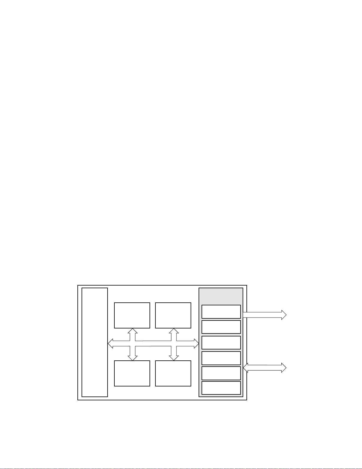
SECTION 1
DEVICE OVERVIEW
The MC68341 is a member of the M68300 family of integrated processors designed
specifically for the compact disc-interactive (CD-I) market. It improves on the feature set of
the MC68340 for a more complete and cost effective integrated system solution to CD-I's
specific needs.
The MC68341 contains a 68020-based CPU32, a two channel DMA controller, two serial
channels, a timer, and a queued serial peripheral interface. The 68341's system
integration module (SIM41) contains clock circuitry, system protection, external bus
interface, timers, and additional chip selects. New to the SIM is the real time clock and an
MC68000 bus interface. The MC68000 bus interface is dynamically selectable to give a
glueless interface to peripherals and memory designed for the MC68000 while allowing
higher performance transfers using the standard 68300 bus interface. Complete code
compatibility with the MC68000 affords the designer access to a broad base of
established real-time kernels, operating systems, languages, applications, and
development tools—many oriented towards embedded control.
As a low voltage part, the MC68341V can operate with a 3.3-V power supply and is
particularly useful for battery applications. MC68341 is used throughout this document to
refer to both the low voltage and standard 5-V parts since both are functionally equivalent.
Figure 1-1 illustrates a block diagram of the MC68341.
SYSTEM
INTEGRATION MODULE
(SIM41)
TIMER
CPU32
(68000-BASED
PROCESSOR)
QUEUED SERIAL
INTERMODULE BUS
PERIPHERAL
INTERFACE
TWO-CHANNEL
DMA CONTROLLER
TWO-CHANNEL
SERIAL I/O
SYSTEM
PROTECTION
CLOCK
SYNTHESIZER
EXTERNAL
BUS INTERFACE
BUS ARBITRATION
REAL TIME CLOCK
IEEE 1149.1 TEST
32-BIT ADDRESS BUS
16-BIT DATA BUS
Figure 1-1. MC68341 Simplified Block Diagram
MOTOROLA MC68341 USER’S MANUAL 1-1

MC68341 FEATURES
The primary features of the MC68341 are as follows:
• High Performance CPU32 Core Processor
— Upward Object-Code Compatible with MC68000 and MC68010
— Additional 32-Bit MC68020 Instructions and Addressing Modes
— Fast Two-Clock Register Instructions
• High-Speed Dual DMA Controllers for Low-Latency Transfers
— 50-Mbyte/Sec Sustained Transfer Rate
— Dual or Single Address Transfers
— 8-, 16-, or 32-Bit Transfers
• Counter/Timer
— 16-Bit Timer with 8-Bit Prescaler
— Multi-mode Operation
— 80 nS Resolution
• Dual Serial Communication Ports
— Synchronous or Asynchronous Operation
— 3-Mbit/Sec Sustained Transfer Rate
— Modem Control
— Baud Rate Generation
— 68681/261 Compatible
• Queued Serial Peripheral Interface (QSPI)
— Communications with Slow Peripherals without Tying Up the CPU
— Queued Transmit and Receive Buffers
— Programmable for Master or Slave SPI Operation
• System Integration Module for Flexible and Cost-Effective System Interface
— 32-Bit Address Bus; 16-Bit Data Bus with Dynamic Bus Sizing
— System Protection, Reset, and Configuration Control
— Periodic Interrupt/System Timer
— Chip-Select, Wait State Generation, Bus Watchdog
— Interrupt Controller
— IEEE 1149.1 Boundary Scan (JTAG)
— Dual 8-Bit Parallel Ports
— Real Time Clock
— Time and Date with Leap Year Correction
— Programmable Alarm for Interrupt or External Output
— Calibration Register Eliminates Need for Trim Capacitor
— Battery Backup Capability
• Power Management
— 5 V or 3.3 V Operation
— Fully Static HCMOS Technology
— Programmable Clock Synthesizer for Full Frequency Control
— Power-Down/Low Power Stop Capabilities
— Idle Modules Can Be Individually Powered Down
• 0–16 or 25 MHz Operation
• 160-Pin Plastic Quad Flat Pack (QFP)
1-2 MC68341 USER’S MANUAL MOTOROLA
 Loading...