

Motorola MC54HC4016AJ, MC74HC4016ADT, MC74HC4016AN Datasheet
SEMICONDUCTOR TECHNICAL DATA
3–1
REV 0
Motorola, Inc. 1995
10/95
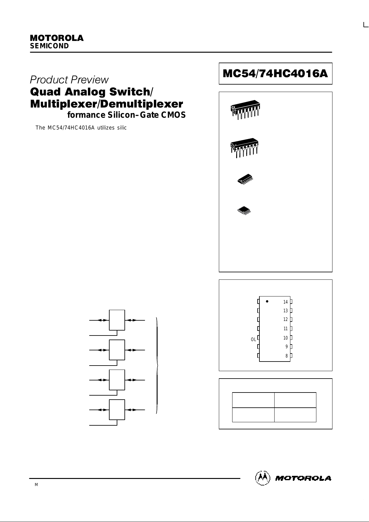
" #!
"!$ "!$
High–Performance Silicon–Gate CMOS
The MC54/74HC4016A u tilizes s ilicon–gate C MOS technology to
achieve fast propagation delays, low ON resistances, and low OFF–
channel leakage current. This bilateral switch/multiplexer/demultiplexer
controls analog and digital v oltages that may vary across t he full
power–supply range (from VCC to GND).
The HC4016A is identical in pinout to the metal–gate CMOS MC14016
and MC14066. Each device has four independent switches. The device
has been designed so that the ON resistances (RON) are much more
linear over input voltage than RON of metal–gate CMOS analog switches.
This device is identical in both function and pinout to the HC4066A. The
ON/OFF Control inputs are compatible with standard CMOS outputs; with
pullup resistors, they are compatible with L STTL outputs. For analog
switches with voltage–level translators, see the HC4316A. For analog
switches with lower RON characteristics, use the HC4066A.
• Fast Switching and Propagation Speeds
• High ON/OFF Output Voltage Ratio
• Low Crosstalk Between Switches
• Diode Protection on All Inputs/Outputs
• Wide Power–Supply Voltage Range (VCC – GND) = 2.0 to 12.0 Volts
• Analog Input Voltage Range (VCC – GND) = 2.0 to 12.0 Volts
• Improved Linearity and Lower ON Resistance over Input Voltage than
the MC14016 or MC14066
• Low Noise
• Chip Complexity: 32 FETs or 8 Equivalent Gates
LOGIC DIAGRAM
1
13
4
5
8
6
11
12
2
3
9
10
A ON/OFF CONTROL
B ON/OFF CONTROL
C ON/OFF CONTROL
D ON/OFF CONTROL
X
A
X
B
X
C
X
D
Y
A
Y
B
Y
C
Y
D
ANALOG
OUTPUTS/INPUTS
ANALOG INPUTS/OUTPUTS = XA, XB, XC, X
D
PIN 14 = V
CC
PIN 7 = GND
This document contains information on a product under development. Motorola reserves the right to change or discontinue this product without notice.
FUNCTION TABLE
PIN ASSIGNMENT
X
B
Y
B
Y
A
X
A
GND
C ON/OFF
CONTROL
B ON/OFF
CONTROL
11
12
13
14
8
9
105
4
3
2
1
7
6
Y
D
X
D
D ON/OFF
CONTROL
A ON/OFF
CONTROL
V
CC
X
C
Y
C
On/Off Control State of
Input Analog Switch
L Off
H On
D SUFFIX
SOIC PACKAGE
CASE 751A–03
N SUFFIX
PLASTIC PACKAGE
CASE 646–06
ORDERING INFORMATION
MC54HCXXXXAJ
MC74HCXXXXAN
MC74HCXXXXAD
MC74HCXXXXADT
Ceramic
Plastic
SOIC
TSSOP
1
14
1
14
J SUFFIX
CERAMIC PACKAGE
CASE 632–08
1
14
1
14
DT SUFFIX
TSSOP PACKAGE
CASE 948G–01
MC54/74HC4016A
MOTOROLA High–Speed CMOS Logic Data
DL129 — Rev 6
3–2
MAXIMUM RATINGS*
Symbol
Parameter
Value
Unit
V
CC
Positive DC Supply Voltage (Referenced to GND)
– 0.5 to + 14.0
V
V
IS
Analog Input Voltage (Referenced to GND)
– 0.5 to VCC + 0.5
V
V
in
Digital Input Voltage (Referenced to GND)
– 0.5 to VCC + 0.5
V
I
DC Current Into or Out of Any Pin
± 25
mA
P
D
Power Dissipation in Still Air,Plastic or Ceramic DIP†
SOIC Package†
TSSOP Package†
750
500
450
mW
T
stg
Storage Temperature
– 65 to + 150
_
C
T
L
Lead Temperature, 1 mm from Case for 10 Seconds
(Plastic DIP, SOIC or TSSOP Package)
(Ceramic DIP)
260
300
_
C
*Maximum Ratings are those values beyond which damage to the device may occur.
Functional operation should be restricted to the Recommended Operating Conditions.
†Derating — Plastic DIP: – 10 mW/_C from 65_ to 125_C
Ceramic DIP: – 10 mW/_C from 100_ to 125_C
SOIC Package: – 7 mW/_C from 65_ to 125_C
TSSOP Package: – 6.1 mW/_C from 65_ to 125_C
For high frequency or heavy load considerations, see Chapter 2 of the Motorola High–Speed CMOS Data Book (DL129/D).
RECOMMENDED OPERATING CONDITIONS
Symbol
Parameter
Min
Max
Unit
V
CC
Positive DC Supply Voltage (Referenced to GND)
2.0
12.0
V
V
IS
Analog Input Voltage (Referenced to GND)
GND
V
CC
V
V
in
Digital Input Voltage (Referenced to GND)
GND
V
CC
V
VIO*
Static or Dynamic Voltage Across Switch
—
1.2
V
T
A
Operating Temperature, All Package Types
– 55
+ 125
_
C
tr, t
f
Input Rise and Fall Time, ON/OFF VCC = 2.0 V
Control Inputs (Figure 10) VCC = 3.0 V
VCC = 4.5 V
VCC = 9.0 V
VCC = 12.0 V
0
0
0
0
0
1000
600
500
400
250
ns
*For voltage drops across the switch greater than 1.2 V (switch on), excessive VCC current may
be drawn; i.e., the current out of the switch may contain both VCC and switch input components.
The reliability of the device will be unaffected unless the Maximum Ratings are exceeded.
DC ELECTRICAL CHARACTERISTICS Digital Section (Voltages Referenced to GND)
Guaranteed Limit
Symbol
Parameter
Test Conditions
V
CC
V
– 55 to
25_C
v
85_Cv 125_C
Unit
V
IH
Minimum High–Level Voltage
ON/OFF Control Inputs
Ron = per spec
2.0
3.0
4.5
9.0
12.0
1.5
2.1
3.15
6.3
8.4
1.5
2.1
3.15
6.3
8.4
1.5
2.1
3.15
6.3
8.4
V
V
IL
Maximum Low–Level Voltage
ON/OFF Control Inputs
Ron = per spec
2.0
3.0
4.5
9.0
12.0
0.5
0.9
1.35
2.70
3.6
0.5
0.9
1.35
2.70
3.6
0.5
0.9
1.35
2.70
3.6
V
This device contains protection
circuitry to guard against damage
due to high static voltages or electric
fields. However, precautions must
be taken to avoid applications of any
voltage higher than maximum rated
voltages to this high–impedance circuit. For proper operation, Vin and
V
out
should be constrained to the
range GND v (Vin or V
out
) v VCC.
Unused inputs must always be
tied to an appropriate logic voltage
level (e.g., either GND or VCC).
Unused outputs must be left open.
I/O pins must be connected to a
properly terminated line or bus.
MC54/74HC4016A
High–Speed CMOS Logic Data
DL129 — Rev 6
3–3 MOTOROLA
DC ELECTRICAL CHARACTERISTICS Digital Section (Voltages Referenced to GND)
Unit
Guaranteed Limit
V
CC
V
Test Conditions
Parameter
Symbol
Unit
v
125_C
v
85_C
– 55 to
25_C
V
CC
V
Test Conditions
Parameter
Symbol
I
in
Maximum Input Leakage Current,
ON/OFF Control Inputs
Vin = VCC or GND
12.0
±0.1
±1.0
±1.0
µA
I
CC
Maximum Quiescent Supply
Current (per Package)
Vin = VCC or GND
VIO = 0 V
6.0
12.0
2
4
20
40
40
160
µA
NOTE: Information on typical parametric values can be found in Chapter 2 of the Motorola High–Speed CMOS Data Book (DL129/D).
DC ELECTRICAL CHARACTERISTICS Analog Section (Voltages Referenced to GND)
Guaranteed Limit
Symbol
Parameter
Test Conditions
V
CC
V
– 55 to
25_C
v
85_Cv 125_C
Unit
R
on
Maximum “ON” Resistance
Vin = V
IH
VIS = VCC to GND
IS v 2.0 mA (Figures 1, 2)
2.0†
4.5
9.0
12.0
—
160
90
90
—
200
110
110
—
240
130
130
Ω
Vin = V
IH
VIS = VCC or GND (Endpoints)
IS v 2.0 mA (Figures 1, 2)
2.0
4.5
9.0
12.0
—
90
70
70
—
115
90
90
—
140
105
105
∆R
on
Maximum Difference in “ON”
Resistance Between Any Two
Channels in the Same Package
Vin V
IH
VIS = 1/2 (VCC – GND)
IS v 2.0 mA
2.0
4.5
9.0
12.0
—
20
15
15
—
25
20
20
—
30
25
25
Ω
I
off
Maximum Off–Channel Leakage
Current, Any One Channel
Vin = V
IL
VIO = VCC or GND
Switch Off (Figure 3)
12.0
0.1
0.5
1.0
µA
I
on
Maximum On–Channel Leakage
Current, Any One Channel
Vin = V
IH
VIS = VCC or GND
(Figure 4)
12.0
0.1
0.5
1.0
µA
†At supply voltage (VCC – GND) approaching 3 V the analog switch–on resistance becomes extremely non–linear. Therefore, for low–voltage
operation, it is recommended that these devices only be used to control digital signals.
NOTE: Information on typical parametric values can be found in Chapter 2 of the Motorola High–Speed CMOS Data Book (DL129/D).
AC ELECTRICAL CHARACTERISTICS (C
L
= 50 pF, ON/OFF Control Inputs: tr = tf = 6 ns)
Guaranteed Limit
Symbol
Parameter
V
CC
V
– 55 to
25_C
v
85_Cv 125_C
Unit
t
PLH
,
t
PHL
Maximum Propagation Delay, Analog Input to Analog Output
(Figures 8 and 9)
2.0
4.5
9.0
12.0
40
5
5
5
50
7
7
7
60
8
8
8
ns
t
PLZ
,
t
PHZ
Maximum Propagation Delay, ON/OFF Control to Analog Output
(Figures 10 and 11)
2.0
4.5
9.0
12.0
80
20
20
20
90
25
25
25
110
35
35
35
ns
t
PZL
,
t
PZH
Maximum Propagation Delay, ON/OFF Control to Analog Output
(Figures 10 and 11)
2.0
4.5
9.0
12.0
80
20
20
20
90
25
25
25
100
30
30
30
ns
MC54/74HC4016A
MOTOROLA High–Speed CMOS Logic Data
DL129 — Rev 6
3–4
AC ELECTRICAL CHARACTERISTICS (C
L
= 50 pF, ON/OFF Control Inputs: tr = tf = 6 ns)
Unit
Guaranteed Limit
V
CC
V
Parameter
Symbol
Unit
v
125_C
v
85_C
– 55 to
25_C
V
CC
V
Parameter
Symbol
C
Maximum Capacitance ON/OFF Control Input
—
10
10
10
pF
Control Input = GND
Analog I/O
Feedthrough
—
—
35
1.0
35
1.0
35
1.0
NOTES:
1. For propagation delays with loads other than 50 pF, see Chapter 2 of the Motorola High–Speed CMOS Data Book (DL129/D).
2. Information on typical parametric values can be found in Chapter 2 of the Motorola High–Speed CMOS Data Book (DL129/D).
Typical @ 25°C, VCC = 5.0 V
C
PD
Power Dissipation Capacitance (Per Switch)* (Figure 13)
15
pF
*Used to determine the no–load dynamic power consumption: PD = CPD V
CC
2
f + ICC VCC. For load considerations, see Chapter 2 of the
Motorola High–Speed CMOS Data Book (DL129/D).
ADDITIONAL APPLICATION CHARACTERISTICS (Voltages Referenced to GND unless noted)
Symbol
Parameter
Test Conditions
V
CC
V
Limit*
25_C
54/74HC
Unit
BW
Maximum On–Channel Bandwidth or
Minimum Frequency Response
(Figure 5)
fin = 1 MHz Sine Wave
Adjust fin Voltage to Obtain 0 dBm at V
OS
Increase fin Frequency Until dB Meter Reads – 3 dB
RL = 50 Ω, CL = 10 pF
4.5
9.0
12.0
150
160
160
MHz
—
Off–Channel Feedthrough Isolation
(Figure 6)
fin Sine Wave
Adjust fin Voltage to Obtain 0 dBm at V
IS
fin = 10 kHz, RL = 600 Ω, CL = 50 pF
4.5
9.0
12.0
– 50
– 50
– 50
dB
fin = 1.0 MHz, RL = 50 Ω, CL = 10 pF
4.5
9.0
12.0
– 40
– 40
– 40
—
Feedthrough Noise, Control to Switch
(Figure 7)
Vin v 1 MHz Square Wave (tr = tf = 6 ns)
Adjust RL at Setup so that IS = 0 A
RL = 600 Ω, CL = 50 pF
4.5
9.0
12.0
60
130
200
mV
PP
RL = 10 kΩ, CL = 10 pF
4.5
9.0
12.0
30
65
100
—
Crosstalk Between Any Two Switches
(Figure 12)
fin Sine Wave
Adjust fin Voltage to Obtain 0 dBm at V
IS
fin = 10 kHz, RL = 600 Ω, CL = 50 pF
4.5
9.0
12.0
– 70
– 70
– 70
dB
fin = 1.0 MHz, RL = 50 Ω, CL = 10 pF
4.5
9.0
12.0
– 80
– 80
– 80
THD
Total Harmonic Distortion
(Figure 14)
fin = 1 kHz, RL = 10 kΩ, CL = 50 pF
THD = THD
Measured
– THD
Source
VIS = 4.0 VPP sine wave
VIS = 8.0 VPP sine wave
VIS = 11.0 VPP sine wave
4.5
9.0
12.0
0.10
0.06
0.04
%
*Guaranteed limits not tested. Determined by design and verified by qualification.
 Loading...