

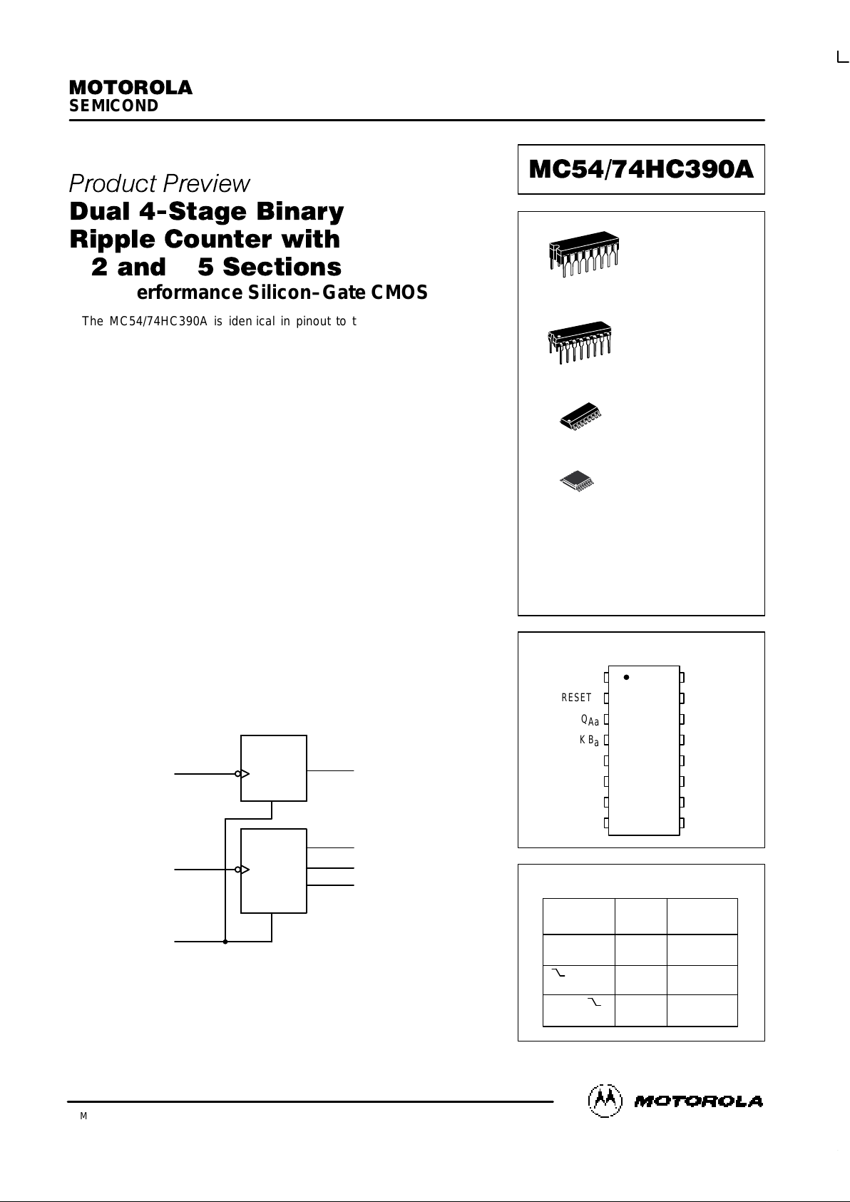
Motorola MC54HC390AJ, MC74HC390AN, MC74HC390AD Datasheet
SEMICONDUCTOR TECHNICAL DATA
1
REV 0
Motorola, Inc. 1995
10/95
$ # !&
$#! %#
÷
÷ #"
High–Performance Silicon–Gate CMOS
The MC54/74HC390A is identical in pinout to the LS390. The device
inputs are compatible with standard CMOS outputs; with pullup resistors,
they are compatible with LSTTL outputs.
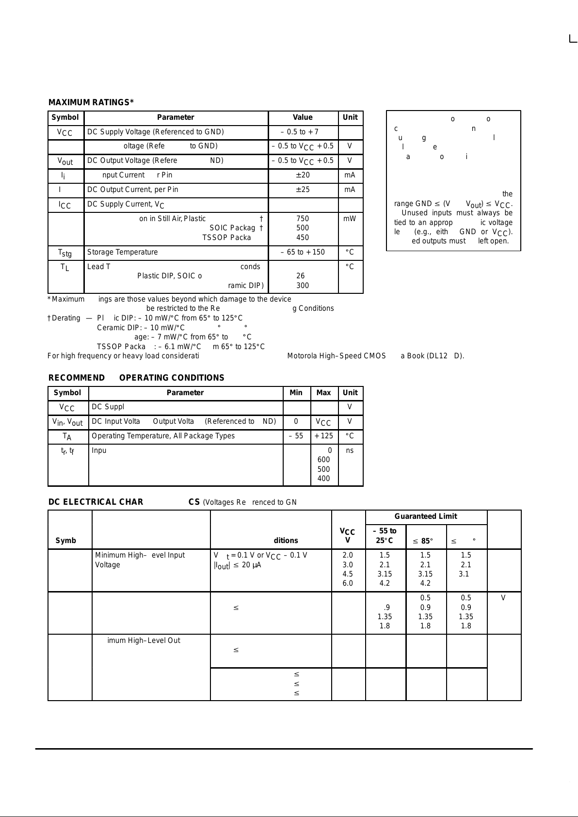
This device consists of two independent 4–bit counters, each composed
of a divide–by–two and a divide–by–five section. The divide–by–two and
divide–by–five counters have separate clock inputs, and can be cascaded to
implement various combinations of ÷ 2 and/or ÷ 5 up to a ÷ 100 counter.
Flip–flops internal to the counters are triggered by high–to–low transitions
of the clock input. A separate, asynchronous reset is provided for each 4–bit
counter. State changes o f the Q outputs do n ot occur simultaneously
because of internal ripple delays. Therefore, decoded output signals are
subject to decoding spikes and should not be used as clocks or strobes
except when gated with the Clock of the HC390A.
• Output Drive Capability: 10 LSTTL Loads
• Outputs Directly Interface to CMOS, NMOS, and TTL
• Operating Voltage Range: 2 to 6 V
• Low Input Current: 1 µA
• High Noise Immunity Characteristic of CMOS Devices
• In Compliance with the Requirements Defined by JEDEC Standard
No 7A
• Chip Complexity: 244 FETs or 61 Equivalent Gates
LOGIC DIAGRAM
Q
A
Q
B
Q
C
Q
D
1, 15
4, 12
2, 14
3, 13
5, 11
6, 10
7, 9
PIN 16 = V
CC
PIN 8 = GND
CLOCK A
RESET
CLOCK B
÷
2
COUNTER
÷
5
COUNTER
This document contains information on a product under development. Motorola reserves the right
to change or discontinue this product without notice.
PIN ASSIGNMENT
13
14
15
16
9
10
11
125
4
3
2
1
8
7
6
CLOCK B
b
Q
Ab
RESET b
CLOCK A
b
V
CC
Q
Db
Q
Cb
Q
Bb
CLOCK B
a
Q
Aa
RESET a
CLOCK A
a
GND
Q
Da
Q
Ca
Q
Ba
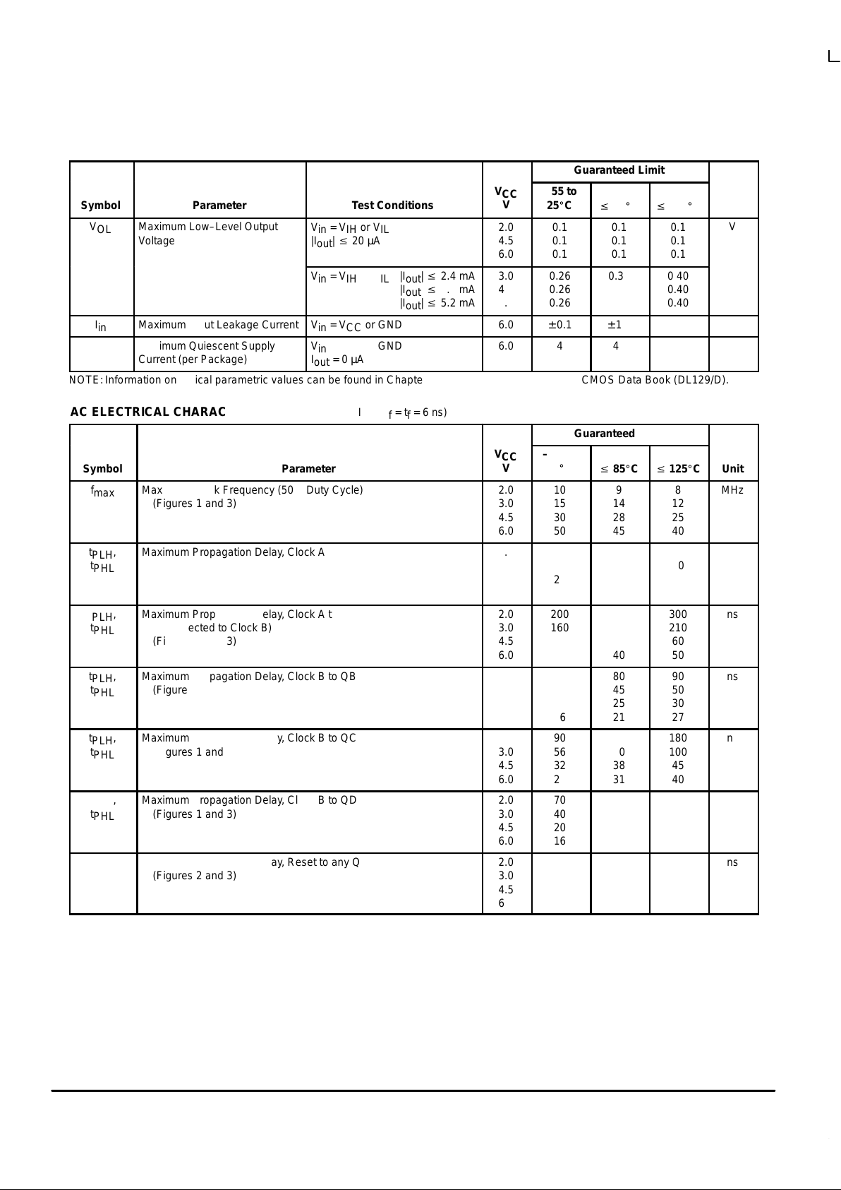
FUNCTION TABLE
Clock
A B Reset Action
X X H Reset
÷ 2 and ÷ 5
X L Increment
÷ 2
X L Increment
÷ 5
D SUFFIX
SOIC PACKAGE
CASE 751B–05
N SUFFIX
PLASTIC PACKAGE
CASE 648–08
ORDERING INFORMATION
MC54HCXXXAJ
MC74HCXXXAN
MC74HCXXXAD
MC74HCXXXADT
Ceramic
Plastic
SOIC
TSSOP
1
16
1
16
J SUFFIX
CERAMIC PACKAGE
CASE 620–10
1
16
1
16
DT SUFFIX
TSSOP PACKAGE
CASE 948F–01
MC54/74HC390A
MOTOROLA High–Speed CMOS Logic Data
DL129 — Rev 6
2
MAXIMUM RATINGS*
Symbol
Parameter
Value
Unit
V
CC
DC Supply Voltage (Referenced to GND)
– 0.5 to + 7.0
V
V
in
DC Input Voltage (Referenced to GND)
– 0.5 to VCC + 0.5
V
V
out
DC Output Voltage (Referenced to GND)
– 0.5 to VCC + 0.5
V
I
in
DC Input Current, per Pin
± 20
mA
I
out
DC Output Current, per Pin
± 25
mA
I
CC
DC Supply Current, VCC and GND Pins
± 50
mA
P
D
Power Dissipation in Still Air,Plastic or Ceramic DIP†
SOIC Package†
TSSOP Package†
750
500
450
mW
T
stg
Storage Temperature
– 65 to + 150
_
C
T
L
Lead Temperature, 1 mm from Case for 10 Seconds
Plastic DIP, SOIC or TSSOP Package
(Ceramic DIP)
260
300
_
C
*Maximum Ratings are those values beyond which damage to the device may occur.
Functional operation should be restricted to the Recommended Operating Conditions.
†Derating — Plastic DIP: – 10 mW/_C from 65_ to 125_C
Ceramic DIP: – 10 mW/_C from 100_ to 125_C
SOIC Package: – 7 mW/_C from 65_ to 125_C
TSSOP Package: – 6.1 mW/_C from 65_ to 125_C
For high frequency or heavy load considerations, see Chapter 2 of the Motorola High–Speed CMOS Data Book (DL129/D).
RECOMMENDED OPERATING CONDITIONS
Symbol
Parameter
Min
Max
Unit
V
CC
DC Supply Voltage (Referenced to GND)
2.0
6.0
V
Vin, V
out
DC Input Voltage, Output Voltage (Referenced to GND)
0
V
CC
V
T
A
Operating Temperature, All Package Types
– 55
+ 125
_
C
tr, t
f
Input Rise and Fall Time VCC = 2.0 V
(Figure 1) VCC = 3.0 V
VCC = 4.5 V
VCC = 6.0 V
0
0
0
0
1000
600
500
400
ns
DC ELECTRICAL CHARACTERISTICS (Voltages Referenced to GND)
Guaranteed Limit
Symbol
Parameter
Test Conditions
V
CC
V
– 55 to
25_C
v
85_Cv 125_C
Unit
V
IH
Minimum High–Level Input
Voltage
V
out
= 0.1 V or VCC – 0.1 V
|I
out
| v 20 µA
2.0
3.0
4.5
6.0
1.5
2.1
3.15
4.2
1.5
2.1
3.15
4.2
1.5
2.1
3.15
4.2
V
V
IL
Maximum Low–Level Input
Voltage
V
out
= 0.1 V or VCC – 0.1 V
|I
out
| v 20 µA
2.0
3.0
4.5
6.0
0.5
0.9
1.35
1.8
0.5
0.9
1.35
1.8
0.5
0.9
1.35
1.8
V
V
OH
Minimum High–Level Output
Voltage
Vin = VIH or V
IL
|I
out
| v 20 µA
2.0
4.5
6.0
1.9
4.4
5.9
1.9
4.4
5.9
1.9
4.4
5.9
V
Vin = VIH or VIL|I
out
| v 2.4 mA
|I
out
| v 4.0 mA
|I
out
| v 5.2 mA
3.0
4.5
6.0
2.48
3.98
5.48
2.34
3.84
5.34
2.20
3.70
5.20
This device contains protection
circuitry to guard against damage
due to high static voltages or electric
fields. However, precautions must
be taken to avoid applications of any
voltage higher than maximum rated
voltages to this high–impedance circuit. For proper operation, Vin and
V
out
should be constrained to the
range GND v (Vin or V
out
) v VCC.
Unused inputs must always be
tied to an appropriate logic voltage
level (e.g., either GND or VCC).
Unused outputs must be left open.
MC54/74HC390A
High–Speed CMOS Logic Data
DL129 — Rev 6
3 MOTOROLA
DC ELECTRICAL CHARACTERISTICS (Voltages Referenced to GND)
Unit
Guaranteed Limit
V
CC
V
Test Conditions
Parameter
Symbol
Unit
v
125_C
v
85_C
– 55 to
25_C
V
CC
V
Test Conditions
Parameter
Symbol
V
OL
Maximum Low–Level Output
Voltage
Vin = VIH or V
IL
|I
out
| v 20 µA
2.0
4.5
6.0
0.1
0.1
0.1
0.1
0.1
0.1
0.1
0.1
0.1
V
Vin = VIH or VIL|I
out
| v 2.4 mA
|I
out
| v 4.0 mA
|I
out
| v 5.2 mA
3.0
4.5
6.0
0.26
0.26
0.26
0.33
0.33
0.33
0.40
0.40
0.40
I
in
Maximum Input Leakage Current
Vin = VCC or GND
6.0
± 0.1
± 1.0
± 1.0
µA
I
CC
Maximum Quiescent Supply
Current (per Package)
Vin = VCC or GND
I
out
= 0 µA
6.0
4
40
160
µA
NOTE: Information on typical parametric values can be found in Chapter 2 of the Motorola High–Speed CMOS Data Book (DL129/D).
AC ELECTRICAL CHARACTERISTICS (C
L
= 50 pF, Input tf = tf = 6 ns)
Guaranteed Limit
Symbol
Parameter
V
CC
V
– 55 to
25_C
v
85_Cv 125_C
Unit
f
max
Maximum Clock Frequency (50% Duty Cycle)
(Figures 1 and 3)
2.0
3.0
4.5
6.0
10
15
30
50
9
14
28
45
8
12
25
40
MHz
t
PLH
,
t
PHL
Maximum Propagation Delay, Clock A to QA
(Figures 1 and 3)
2.0
3.0
4.5
6.0
70
40
20
16
80
45
25
21
90
50
30
27
ns
t
PLH
,
t
PHL
Maximum Propagation Delay, Clock A to QC
(QA connected to Clock B)
(Figures 1 and 3)
2.0
3.0
4.5
6.0
200
160
35
30
250
185
45
40
300
210
60
50
ns
t
PLH
,
t
PHL
Maximum Propagation Delay, Clock B to QB
(Figures 1 and 3)
2.0
3.0
4.5
6.0
70
40
20
16
80
45
25
21
90
50
30
27
ns
t
PLH
,
t
PHL
Maximum Propagation Delay, Clock B to QC
(Figures 1 and 3)
2.0
3.0
4.5
6.0
90
56
32
25
105
70
38
31
180
100
45
40
ns
t
PLH
,
t
PHL
Maximum Propagation Delay, Clock B to QD
(Figures 1 and 3)
2.0
3.0
4.5
6.0
70
40
20
16
80
45
25
21
90
50
30
27
ns
t
PHL
Maximum Propagation Delay, Reset to any Q
(Figures 2 and 3)
2.0
3.0
4.5
6.0
80
48
28
21
95
65
32
25
110
75
40
30
ns
 Loading...