

Motorola MC54HC354J, MC74HC354N Datasheet
SEMICONDUCTOR TECHNICAL DATA
1
REV 7
Motorola, Inc. 1995
10/95
"! ! !
"!# ! !
!
!! "!"!
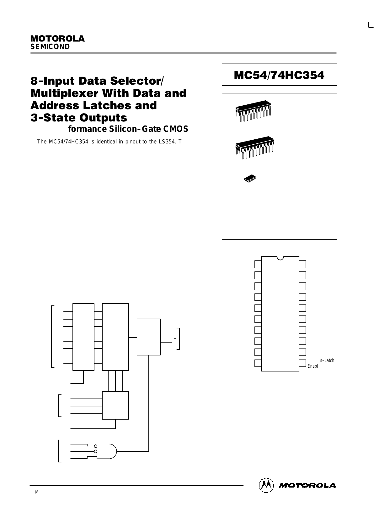
High–Performance Silicon–Gate CMOS
The MC54/74HC354 is identical in pinout to the LS354. The device
inputs are compatible with Standard CMOS outputs; with pullup resistors,
they are compatible with LSTTL outputs.
The HC354 selects one of eight latched binary Data Inputs, as determined by the Address Inputs. The information at the Data Inputs is stored
in the transparent 8–bit Data Latch when the Data–Latch Enable pin is
held high. The Address information may be stored in the transparent
Address Latch, which is enabled by the active–high Address–Enable pin.
The device outputs are placed in high–impedance states when Output
Enable 1 is high, Output Enable 2 is high, or Output Enable 3 is low.
The HC354 has a clocked Data Latch that is not transparent.
• Output Drive Capability: 15 LSTTL Loads
• Outputs Directly Interface to CMOS, NMOS and TTL
• Operating Voltage Range: 2 to 6V
• Low Input Current: 1µA
• High Noise Immunity Characteristic of CMOS Devices
• In Compliance With the JEDEC Standard No. 7A Requirements
• Chip Complexity: 326 FETs or 81.5 Equivalent Gates
LOGIC DIAGRAM
D0
8
D1
7
D2
6
D3
5
D4
4
D5
3
D6
2
D7
1
8–BIT
DATA
LATCH
(TRANS–
PARENT)
8–BIT
MULTI–
PLEXER
DATA
INPUTS
3–STATE
OUTPUT
CONTROL
Y
19
Y
18
3–STATE
DATA
OUTPUTS
DATA–LATCH
ENABLE
9
A0
14
A1
13
A2
12
ADDRESS
INPUTS
ADDRESS–LATCH
ENABLE
11
OE1
15
OE2
16
OE3
17
OUTPUT
ENABLES
ADDRESS
LATCH
(TRANS–
PARENT)
PIN 20 = V
CC
PIN 10 = GND
201
192
183
174
V
CC
D7
165
156
147
138
129
1110
YD6
Y
D5
OE3D4
OE2D3
OE1D2
A0D1
A1D0
A2
Data–Latch
Enable
Address–Latch
Enable
GND
Pinout: 20–Lead Package (Top View)
DW SUFFIX
SOIC PACKAGE
CASE 751D–04
N SUFFIX
PLASTIC PACKAGE
CASE 738–03
ORDERING INFORMATION
MC54HCXXXJ
MC74HCXXXN
MC74HCXXXDW
Ceramic
Plastic
SOIC
J SUFFIX
CERAMIC PACKAGE
CASE 732–03
1
20
1
20
1
20
MC54/74HC354
MOTOROLA High–Speed CMOS Logic Data
DL129 — Rev 6
2
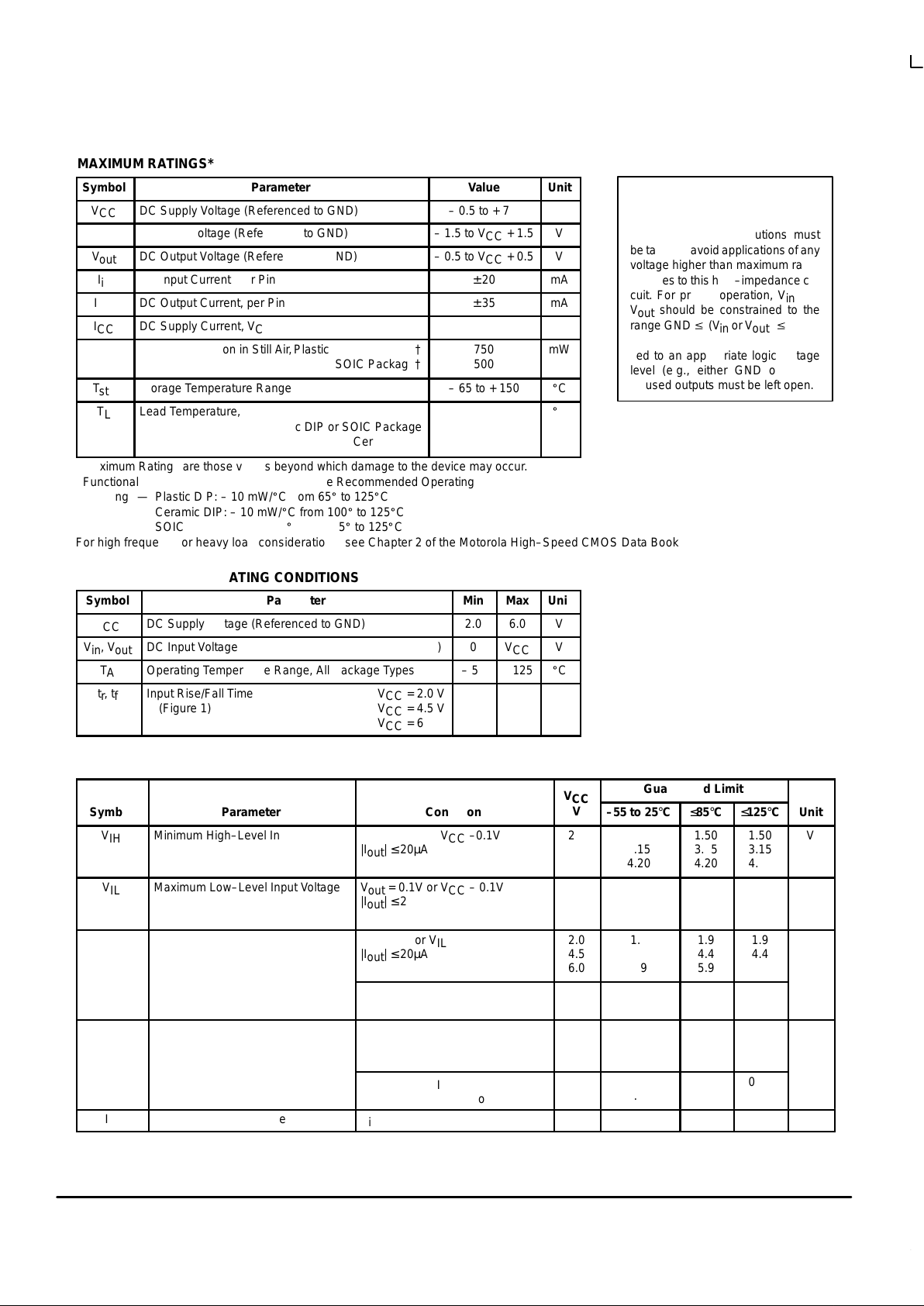
MAXIMUM RATINGS*
Symbol
Parameter
Value
Unit
V
CC
DC Supply Voltage (Referenced to GND)
– 0.5 to + 7.0
V
V
in
DC Input Voltage (Referenced to GND)
– 1.5 to VCC + 1.5
V
V
out
DC Output Voltage (Referenced to GND)
– 0.5 to VCC + 0.5
V
I
in
DC Input Current, per Pin
± 20
mA
I
out
DC Output Current, per Pin
± 35
mA
I
CC
DC Supply Current, VCC and GND Pins
± 75
mA
P
D
Power Dissipation in Still Air,Plastic or Ceramic DIP†
SOIC Package†
750
500
mW
T
stg
Storage Temperature Range
– 65 to + 150
_
C
T
L
Lead Temperature, 1 mm from Case for 10 Seconds
Plastic DIP or SOIC Package
Ceramic DIP
260
300
_
C
*Maximum Ratings are those values beyond which damage to the device may occur.
Functional operation should be restricted to the Recommended Operating Conditions.
†Derating — Plastic DIP: – 10 mW/_C from 65_ to 125_C
Ceramic DIP: – 10 mW/_C from 100_ to 125_C
SOIC Package: – 7 mW/_C from 65_ to 125_C
For high frequency or heavy load considerations, see Chapter 2 of the Motorola High–Speed CMOS Data Book (DL129/D).
RECOMMENDED OPERATING CONDITIONS
Symbol
Parameter
Min
Max
Unit
V
CC
DC Supply Voltage (Referenced to GND)
2.0
6.0
V
Vin, V
out
DC Input Voltage, Output Voltage (Referenced to GND)
0
V
CC
V
T
A
Operating Temperature Range, All Package Types
– 55
+ 125
_
C
tr, t
f
Input Rise/Fall Time VCC = 2.0 V
(Figure 1) VCC = 4.5 V
VCC = 6.0 V
0
0
0
1000
500
400
ns
DC CHARACTERISTICS (Voltages Referenced to GND)
V
Guaranteed Limit
Symbol
Parameter
Condition
V
CC
V
–55 to 25°C ≤85°C ≤125°C
Unit
V
IH
Minimum High–Level Input Voltage V
out
= 0.1V or VCC –0.1V
|I
out
| ≤ 20µA
2.0
4.5
6.0
1.50
3.15
4.20
1.50
3.15
4.20
1.50
3.15
4.20
V
V
IL
Maximum Low–Level Input Voltage V
out
= 0.1V or VCC – 0.1V
|I
out
| ≤ 20µA
2.0
4.5
6.0
0.3
0.9
1.2
0.3
0.9
1.2
0.3
0.9
1.2
V
V
OH
Minimum High–Level Output
Voltage
Vin = VIH or V
IL
|I
out
| ≤ 20µA
2.0
4.5
6.0
1.9
4.4
5.9
1.9
4.4
5.9
1.9
4.4
5.9
V
Vin =VIH or V
IL
|I
out
| ≤ 6.0mA
|I
out
| ≤ 7.8mA
4.5
6.0
3.98
5.48
3.84
5.34
3.70
5.20
V
OL
Maximum Low–Level Output
Voltage
Vin = VIH or V
IL
|I
out
| ≤ 20µA
2.0
4.5
6.0
0.1
0.1
0.1
0.1
0.1
0.1
0.1
0.1
0.1
V
Vin = VIH or V
IL
|I
out
| ≤ 6.0mA
|I
out
| ≤ 7.8mA
4.5
6.0
0.26
0.26
0.33
0.33
0.40
0.40
I
in
Maximum Input Leakage Current Vin = VCC or GND 6.0 ±0.1 ±1.0 ±1.0 µA
This device contains protection
circuitry to guard against damage
due to high static voltages or electric
fields. However, precautions must
be taken to avoid applications of any
voltage higher than maximum rated
voltages to this high–impedance circuit. For proper operation, Vin and
V
out
should be constrained to the
range GND v (Vin or V
out
) v VCC.
Unused inputs must always be
tied to an appropriate logic voltage
level (e.g., either GND or VCC).
Unused outputs must be left open.
MC54/74HC354
High–Speed CMOS Logic Data
DL129 — Rev 6
3 MOTOROLA
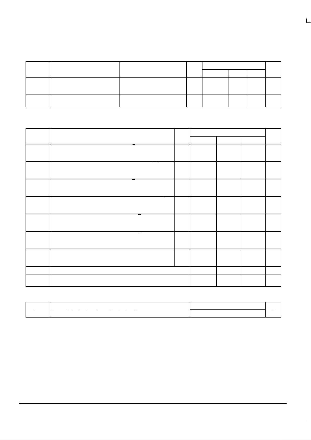
DC CHARACTERISTICS (Voltages Referenced to GND)
Symbol Unit
Guaranteed Limit
V
CC
V
ConditionParameter
Symbol Unit≤125°C≤85°C–55 to 25°C
V
CC
V
ConditionParameter
I
OZ
Maximum Three–State Leakage
Current
Output in High–Impedance State
Vin = VIL or V
IH
V
out
= VCC or GND
6.0 ±0.5 ±5.0 ±10.0 µA
I
CC
Maximum Quiescent Supply
Current (per Package)
Vin = VCC or GND
I
out
= 0µA
6.0 8 80 160 µA
NOTE: Information on typical parametric values can be found in Chapter 2 of the Motorola High–Speed CMOS Data Book (DL129/D).
AC CHARACTERISTICS (C
L
= 50 pF, Input tr = tf = 6 ns)
Guaranteed Limit
Symbol
Parameter
V
CC
V
–55 to 25°C ≤85°C ≤125°C
Unit
t
PLH
,
t
PHL
Maximum Propagation Delay, D0–D7 to Y or Y
(Figures 2 and 6)
2.0
4.5
6.0
210
42
36
265
53
45
315
63
54
ns
t
PLH
,
t
PHL
Maximum Propagation Delay, Data–Latch Enable to Y or Y
(Figures 3 and 6)
2.0
4.5
6.0
260
52
44
325
65
55
390
78
66
ns
t
PLH
,
t
PHL
Maximum Propagation Delay, A0–A2 to Y or Y
(Figures 2 and 6)
2.0
4.5
6.0
270
54
46
340
68
58
405
81
69
ns
t
PLH
,
t
PHL
Maximum Propagation Delay, Address–Latch Enable to Y or Y
(Figures 3 and 6)
2.0
4.5
6.0
270
54
46
340
68
58
405
81
69
ns
t
PLZ
,
t
PHZ
Maximum Propagation Delay, OE1–OE3 to Y or Y
(Figures 4 and 7)
2.0
4.5
6.0
160
32
27
200
40
34
240
48
41
ns
t
PZL
,
t
PZH
Maximum Propagation Delay, OE1–OE3 to Y or Y
(Figures 4 and 7)
2.0
4.5
6.0
125
25
21
155
31
26
190
38
32
ns
t
TLH
,
t
THL
Maximum Output Transition Time, Any Output
(Figures 1 and 6)
2.0
4.5
6.0
60
12
10
75
15
13
90
18
15
ns
C
in
Maximum Input Capacitance 10 10 10 pF
C
out
Maximum Three–State Output Capacitance (Output in High Impedance
State)
15 15 15 pF
NOTE: For propagation delays with loads other than 50 pF, and information on typical parametric values, see Chapter 2 of the Motorola High–
Speed CMOS Data Book (DL129/D).
Typical @ 25°C, VCC = 5.0 V
C
PD
Power Dissipation Capacitance (Per Package)*
48
pF
*Used to determine the no–load dynamic power consumption: PD = CPD V
CC
2
f + ICC VCC. For load considerations, see Chapter 2 of the
Motorola High–Speed CMOS Data Book (DL129/D).
 Loading...