

MOTOROLA MC4558CP1, MC4558CDR2, MC4558VP1, MC4558VDR2, MC4558VD Datasheet
Device
Operating
Temperature Range
Package
SEMICONDUCTOR
TECHNICAL DATA
DUAL WIDE BANDWIDTH
OPERATIONAL AMPLIFIERS
ORDERING INFORMATION
MC4558CD
MC4558ACP1,CP1
TA = 0° to +70°C
SO–8
Plastic DIP
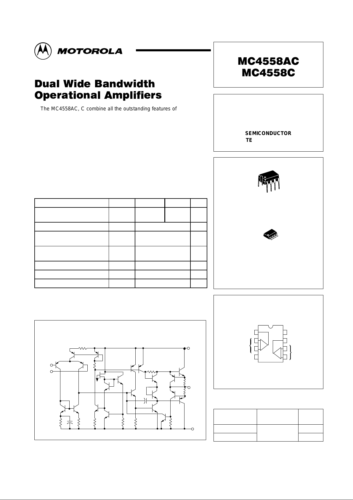
PIN CONNECTIONS
Order this document by MC4558AC/D
P1 SUFFIX
PLASTIC PACKAGE
CASE 626
D SUFFIX
PLASTIC PACKAGE
CASE 751
(SO–8)
1
1
8
8
(Top View)
V
EE
Inputs A
Inputs B
Output B
Output A
V
CC
–
–
+
+
1
2
3
4
8
7
6
5
B
A
1
MOTOROLA ANALOG IC DEVICE DATA
The MC4558AC, C combine all the outstanding features of the MC1458
and, in addition offer three times the unity gain bandwidth of the industry
standard.
• 2.5 MHz Unity Gain Bandwidth Guaranteed (MC4558AC)
• 2.0 MHz Unity Gain Bandwidth Guaranteed (MC4558C)
• Internally Compensated
• Short Circuit Protection
• Gain and Phase Match between Amplifiers
• Low Power Consumption
MAXIMUM RATINGS
(TA = +25°C, unless otherwise noted.)
Rating Symbol MC4558AC MC4558C Unit
Power Supply Voltage V
CC
V
EE
+22
–22
+18
–18
Vdc
Input Differential Voltage V
ID
±30 V
Input Common Mode Voltage
(Note 1)
V
ICM
±15 V
Output Short Circuit Duration
(Note 2)
t
SC
Continuous
Ambient Temperature Range T
A
0 to +70 °C
Storage Temperature Range T
stg
–55 to +125 °C
Junction Temperature T
J
150 °C
NOTES: 1.For supply voltages less than ±15 V, the absolute maximum input voltage is equal
to the supply voltage.
2.Short circuit may be to ground or either supply.
Representative Schematic Diagram
(1/2 of Circuit Shown)
2.9 k
V
CC
25
Output
25
V
EE
150
620
Inverting
Input –
+
Noninverting
Input
5.0 k 53
pF
680
1.84 k 20 k 50 k
10 pF
5.0 k
Motorola, Inc. 1996 Rev 5
MC4558AC MC4558C
2
MOTOROLA ANALOG IC DEVICE DATA
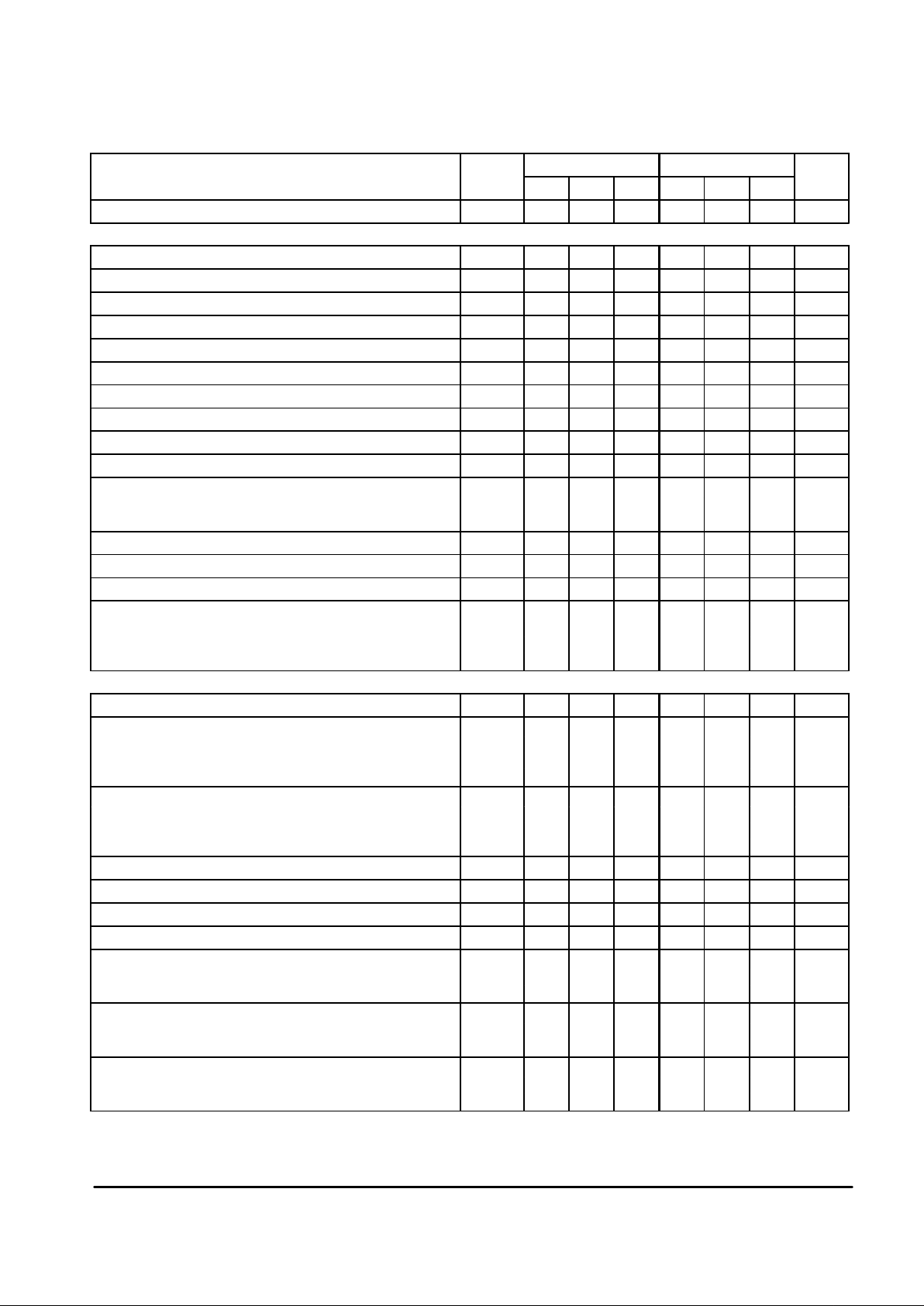
FREQUENCY CHARACTERISTICS (V
CC
= +15 V , VEE = –15 V , TA = 25°C)
MC4558AC MC4558C
Characteristic Symbol
Min Typ Max Min Typ Max
Unit
Unity Gain Bandwidth BW 2.5 2.8 – 2.0 2.8 – MHz
ELECTRICAL CHARACTERISTICS (V
CC
= 15 V, VEE = –15 V , TA = 25°C, unless otherwise noted.)
Input Offset Voltage (RS ≤ 10 kΩ) V
IO
– 1.0 5.0 – 2.0 6.0 mV
Input Offset Current I
IO
– 20 200 – 20 200 nA
Input Bias Current (Note 1) I
IB
– 80 500 – 80 500 nA
Input Resistance r
i
0.3 2.0 – 0.3 2.0 – MΩ
Input Capacitance C
i
– 1.4 – – 1.4 – pF
Common Mode Input Voltage Range V
ICR
±12 ±13 – ±12 ±13 – V
Large Signal Voltage Gain (VO = ±10 V, RL = 2.0 kΩ) A
VOL
50 200 – 20 200 – V/mV
Output Resistance r
o
– 75 – – 75 – Ω
Common Mode Rejection (RS ≤ 10 kΩ) CMR 70 90 – 70 90 – dB
Supply Voltage Rejection Ratio (RS ≤ 10 kΩ) PSRR – 30 150 – 30 150 µV/V
Output Voltage Swing V
O
V
(RL ≥ 10 kΩ) ±12 ±14 – ±12 ±14 –
(RL ≥ 2.0 kΩ) ±10 ±13 – ±10 ±13 –
Output Short Circuit Current I
SC
10 20 40 10 20 40 mA
Supply Currents (Both Amplifiers) I
D
– 2.3 5.0 – 2.3 5.6 mA
Power Consumption (Both Amplifiers) P
C
– 70 150 – 70 170 mW
Transient Response (Unity Gain)
(VI = 20 mV, RL ≥ 2.0 kΩ, CL ≤ 100 pF) Rise Time t
TLH
– 0.3 – – 0.3 – µs
(VI = 20 mV, RL ≥ 2.0 kΩ, CL ≤ 100 pF) Overshoot os – 15 – – 15 – %
(VI = 10 V, RL ≥ 2.0 kΩ, CL ≤ 100 pF) Slew Rate SR 1.5 1.6 – 1.0 1.6 – V/µs
ELECTRICAL CHARACTERISTICS (V
CC
= +15 V , VEE = –15 V , TA = T
high
to T
low
, unless otherwise noted. See Note 2.)
Input Offset Voltage (RS ≤ 10 kΩ) V
IO
– 1.0 6.0 – – 7.5 mV
Input Offset Current I
IO
nA
(TA = T
high
) – 7.0 200 – – –
(TA = T
low
) – 85 500 – – –
(TA = 0° to +70°C) – – – – – 300
Input Bias Current I
IB
nA
(TA = T
high
) – 30 500 – – –
(TA = T
low
) – 300 1500 – – –
(TA = 0° to +70°C) – – – – – 800
Common Mode Input Voltage Range V
ICR
±12 ±13 – – – – V
Large Signal Voltage Gain (VO = ±10 V, RL = 2.0 kΩ) A
VOL
25 – – 15 – – V/mV
Common Mode Rejection (RS ≤ 10 kΩ) CMR 70 90 – – – – dB
Supply Voltage Rejection Ratio (RS ≤ 10 kΩ) PSRR – 30 150 – – – µV/V
Output Voltage Swing V
O
V
(RL ≥ 10 kΩ) ±12 ±14 – ±12 ±14 –
(RL ≥ 2.0 kΩ) ±10 ±13 – ±10 ±13 –
Supply Currents (Both Amplifiers) I
D
mA
(TA = T
high
) – – 4.5 – – 5.0
(TA = T
low
) – – 6.0 – – 6.7
Power Consumption (Both Amplifiers) P
C
mW
(TA = T
high
) – – 135 – – 150
(TA = T
low
) – – 180 – – 200
NOTES: 1.IIB is out of the amplifier due to PNP input transistors.
2.T
high
= +70°C, T
low
= 0°C.
MC4558AC MC4558C
3
MOTOROLA ANALOG IC DEVICE DATA
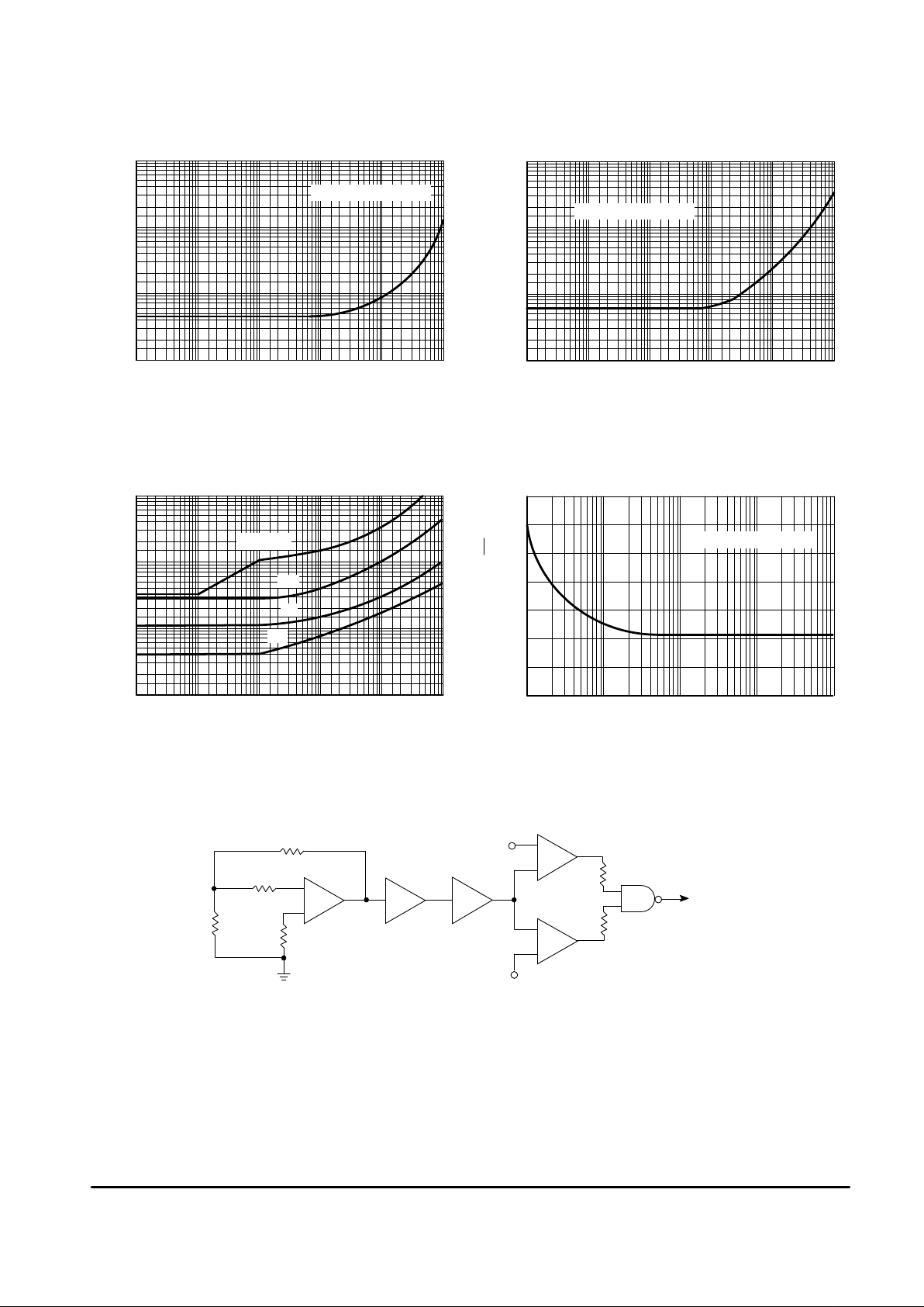
Figure 1. Burst Noise versus Source Resistance Figure 2. RMS Noise versus Source Resistance
Figure 3. Output Noise versus Source Resistance Figure 4. Spectral Noise Density
Figure 5. Burst Noise Test Circuit
Unlike conventional peak reading or RMS meters, this system was
especially designed to provide the quick response time essential
to burst (popcorn) noise testing.
The test time employed is 10 sec and the 20 µV peak limit
refers to the operational amplifier input thus eliminating errors
in the closed loop gain factor of the operational amplifier.
RS, SOURCE RESISTANCE (Ω)
0
10
100
1000
10 100 1.0 k 10 k 100 k 1.0 M
BW = 1.0 Hz to 1.0 kHz
e
n
,INPUT NOISE (Peak) ( V)
µ
e
n
, INPUT NOISE (Peak) ( V)
µ
RS, SOURCE RESISTANCE (Ω)
0.1
1.0
10
100
10 100 1.0 10 k 100 k 1.0 M
BW = 1.0 Hz to 1.0 kHz
OUTPUT NOISE (RMS) (mV)
RS, SOURCE RESISTANCE (Ω)
0.01
0.1
1.0
10
10 100 1.0 k 10 k 100 k 1.0 M
AV = 1000
10
1.0
e
n
,
100
f, FREQUENCY (Hz)
10 100 1.0 k 100 k10 k
140
120
100
80
40
20
0
60
AV = 10, RS = 100 k
Ω
INPUT NOISE (
nV/
Hz
√
)
+
1.0 k
Operational Amplifier
Under Test
Low Pass Filter
1.0 Hz to 1.0 kHz
100 k
X 500 X 2
To Pass / Fail
Indicator
–
100 k
100 k
+
+
–
–
Positive
Threshold
Voltage
Negative
Threshold
Voltage
e
n
,
 Loading...