

查询MC44BC375供应商
Technical Data
MC44BC375/D
Rev. 2.6 01/2003
Freescale Semiconductor, Inc.
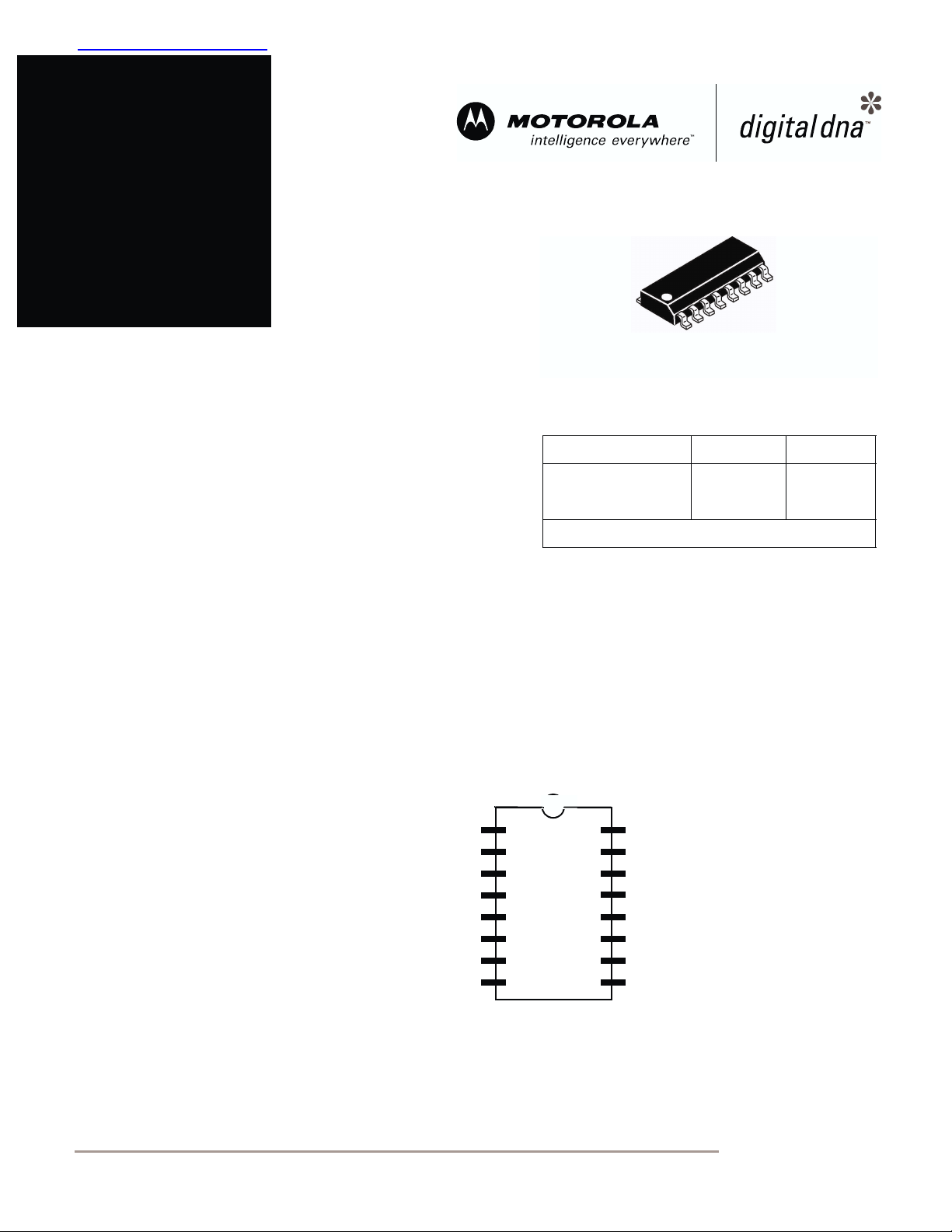
MC44BC375/U/J/T
PLL Tuned VHF Audio/
Video High Integration
Modulator ICs
nc...
I
Contents List
1 Features ............. 2
2 DeviceOverview ......3
3 MaximumRatings .....4
4 ThermalRating .......4
5 Electrostatic Discharge 4
6Electrical
Characteristics 5
7 PinSelection ......... 6
8 High Frequency
Characteristics
cale Semiconductor,
Frees
(U Version) 6
9 Video Characteristics . . 7
10 Audio Characteristics . . 7
11 Characterization
Measurement
Conditions 7
12 Modulator
Functionality 11
13 Pin Circuit Schematics 14
14 MC44BC375U Application
Schematic 15
15 Markings and Case
Diagrams 16
MC44BC375/U/J/T
SO16 Package
Ordering Information
Device Temp. Range Package
MC44BC375UD, R2
MC44BC375JD, R2
MC44BC375TD, R2
NOTE: For tape and reel, add R2 suffix.
This modulator circuit is for use in VCRs, set top boxes and similar devices. The device
differences are as follows:
• MC44BC375U VHF [CH3 & CH4] (Americas)
• MC44BC375J VHF [CH1 & CH2] (Japan)
• MC44BC375T VHF [CH13] (Taiwan)
CHS
PSS
LOP
XTAL
GND
PREEM
AUDIO
SPLFLT
1
2
3
4
5
6
7
8
16
15
14
13
12
11
10
9
SFS
PLLFLT
TVOVCC
TVOUT
GND
VCCA
VIDEO
PSave/LO
-20°C to +85°C SO16NB
Figure 1. MC44BC375U/J/T Pin Connection Diagram
This document contains information on a product under development. Motorola reserves the right to change or
discontinue this product without notice. © Motorola, Inc., 2002. All rights reserved.
For More Information On This Product,
Go to: www.freescale.com

Features
Freescale Semiconductor, Inc.
1 Features
Channels are selectable using pin Channel Selection (CHS) and tuned by a PLL. They do not require any
external tank circuit components thus reducing the sensitivity of the PCB design and the need for external
adjustments. The PLL obtains its reference from a 4MHz crystal oscillator.
The sound subcarrier is also generated on-chip without external components. The 4.5MHz or 5.5MHz
Sound frequency is selectable using pin Sound Frequency Selection (SFS). The Pictureto Sound subcarrier
ratio is also selectable by pin Picture to Sound selection (PSS) to either 14dB or 16dB. A Power Save
function is selectable via pin Psave/LO which turns off all internal VCOs and mixers and simultaneously
switches ON the Logic Output Port (LOP). No external Varicap Diodes/ Inductor nor other tuned
components are needed.
The MC44BC375/U/J/T also has the following features:
• Channel selected by CHS pin
• Integrated On-Chip Oscillator - No external tank circuit
• Extremely Low External Components Count
nc...
I
cale Semiconductor,
Frees
• Adjustable Video Modulation Depth ( 85% w/o adjustment)
•PeakWhiteClip
• Programmable Picture/Sound Carrier Ratio (14dB & 16dB) selected by PSS pin
•IntegratedOnNo external varicaps
• Modulator Standby Mode selected by Psave/LO pin
• Transient Output Inhibit During PLL Lock-up at Power-on
• Logic Output Port selected by Psave/LO pin (Antenna Switch Driver)
• Extremely Robust ESD protection, Minimum 4kV, typical 6kV.
• Available in 80 dBuV RF output level (MC44BC375UA).
chipProgrammableSound Subcarrier Oscillator (4.5 & 5.5MHzselectedby SFS pin)
2 MC44BC375/U/J/T Technical Data MOTOROLA
For More Information On This Product,
Go to: www.freescale.com
M
O
Freescale Semiconductor, Inc.
Device Overview
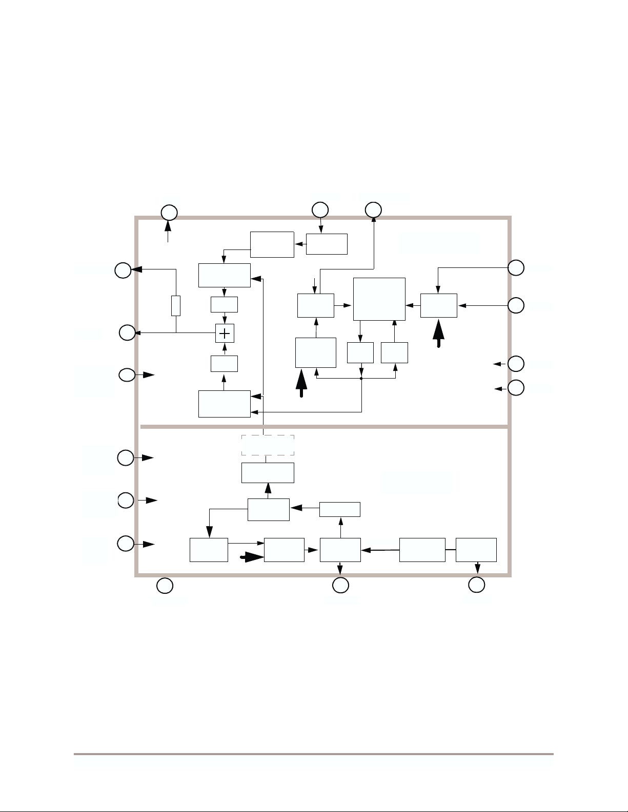
2 Device Overview
Figure 2 shows a simplified block diagram of the MC44BC375U/J/Tdevice.
The MC44BC375U/J/T device has two main sections:
1. A modulator section which accepts audio and video inputs and modulates the VHF carrier.
2. A PLL section to synthesize the UHF/VHF output channel frequency (from an integrated
UHF oscillator, divided for VHF output)
The high frequency BICMOS technology permits integration of tank circuit and certain filtering functions.
nc...
I
cale Semiconductor,
Frees
VOVCC
VOUT
ower
ave
save/
OP
Snd Freq
Select
-SFS
Channel
Select CHS
PS1/2
Select
-PSS
14
16
13
9
1
2
75
LOP
3
Ω
Video
Modulator
LPF
LPF
Sound
Modulator
Prescaler
/8
CHS
Peak
White Clip
31.25kHz
Test Mode
Divider
VHF
Divider
UHF
OSC.
Prog.
Divider
Divider
SFS
VIDEO
10
Clamp
Sound
PFD
Prog.
PLL
Phase
Comp.
SPLLFLT
8
Sound
Oscillator
and FM
Modulator
LPF ALC
VCO & PLL
31.25kHz
MODULATOR
SECTION
Audio
Ampli
PSS
SECTION
Ref Divider
/128
4Mhz
XCO
7
6
11
5
AUDI
PREE
VCCA
GND
12
GND
Figure 2. MC44BC375/U/J/T Block Diagram
MOTOROLA MC44BC375/U/J/T Technical Data 3
For More Information On This Product,
Go to: www.freescale.com
15
PLLFLT
4
XTAL
Maximum Ratings
Freescale Semiconductor, Inc.
3 Maximum Ratings
Sym Parameter Value Unit
Vcc Supply voltage 6 V
Tamin Minimum operating ambient temperature –20
Tamax Maximum operating ambient temperature 85
Tstgmin Minimum storage temperature –65
Tstgmax Maximum storage temperature 150
Tj Junction Temperature 150 °C
Maximum ratings are those values beyond which damage to the device may occur. For functional operation, values
should be restricted to the Recommended Operating Condition.
Meets Moisture Sensitivity Level 1, no dry pack required.
nc...
I
4 Thermal Rating
Sym Parameter Value Unit
R
Thermal resistance from Junction to Ambient 140 °C/W
thja
o
o
o
o
This device contains protection circuitry to guard
against damage due to high static voltage or electric
fields. However, precautions must be taken to avoid
C
applications of any voltage higher than maximum rated
C
voltages to this high impedance circuit. For proper
operation, input and output voltages should be
C
constrained to the ranges indicated in the
C
Recommended Operating Conditions.
5 Electrostatic Discharge
Electrostatic Discharge (ESD) tests are done on all pins.
Sym Parameter Min Typ Unit
ESD
MM (Machine Model) - MIL STD 883C method 3015-7 200 500 V
ESD
HBM (Human Body Model) - MIL STD 883C method 3015-7 4000 6000 V
cale Semiconductor,
Frees
4 MC44BC375/U/J/T Technical Data MOTOROLA
For More Information On This Product,
Go to: www.freescale.com
Freescale Semiconductor, Inc.
Electrical Characteristics
6 Electrical Characteristics
• A = 100% Tested
• B = 100% Correlation tested
• C = Characterized on samples
• D = Design parameter
6.1 Specification Conditions
Unless otherwise stated: Vcc = 5.0V, T amb. = 25°C.Video input 1Vp-p, 10 step greyscale. RF inputs /
outputs into 75Ω load. SPECIFICATIONS ONLY VALID FOR ENVELOPE DEMODULATION
Power Supply Parameters Min Typ Max Unit Notes Type
Operating Supply Voltage range 4.5 5.0 5.5 V B
Total Supply Current 40 47 55 mA All sections active A
nc...
I
Total Standby Mode Supply Current 3 5 7 mA PSave/LO=LO A
cale Semiconductor,
Frees
DC Parameter Min Typ Max Unit Type
Threshold voltage level on pins CHS, PSS, SFS, PSave/LO 2.1 V C
Sound Comparator Charge Pump Current: During locking
When locked
RF Comparator Charge Pump Current 60 100 150 µA A
Crystal Oscillator Stability - negative resistance 1 - - KΩ D
Logic Output Port: Saturation voltage @ I=15mA
Leakage current
71012µA A
0.7 1 1.5 µA A
--210-3001mV
uA
A
A
MOTOROLA MC44BC375/U/J/T Technical Data 5
For More Information On This Product,
Go to: www.freescale.com
Pin Selection
Freescale Semiconductor, Inc.
7 Pin Selection
Pin Nb Pin Name Device LO (grounded) HI (Open or +5V)
MC44BC375U
1 CHS
2 PSS MC44BC375U/J/T 14dB 16dB
9 PSave/LO MC44BC375U/J/T
16 SFS MC44BC375U/J/T 5.5Mhz 4.5Mhz
MC44BC375J
MC44BC375T
By default (open condition), all pins are “HI”.
7.1 Test Modes
Pin DC level Description
Vcc + 0.3V
nc...
I
CHS
Vcc + 1.1V
PSS Vcc + 1Vbe Transient Output Inhibit Disabled
SFS Vcc + 1Vbe Sound Oscillator OFF
VIDEO
Vcc + 0.3V
Vcc + 1.1V
Low frequency testing (RF frequency divided by 4 for MC44BC375U/J, and
divided by 8 for MC44BC375T)
Base band test mode (DC drive applied to modulators)
Force UHF and Sound PLL Upper current source
Force UHF and Sound PLL Lower current source
CH4
CH2
CH13
Power save Mode
LOP pin LO (Low voltage)
CH3
CH1
CH13
Normal Operation
LOP pin HI (High impedance
cale Semiconductor,
Frees
NOTE:
Test modes are intended for m anufacturing test purpose only and not to be
be used for normal application.
8 High Frequency Characteristics (U Version)
For all the following specifications and unless otherwise stated: Vcc = 5.0V, T amb. = 25°C.Video input
1Vp-p, 10 step greyscale.RF inputs / outputs into 75
ENVELOPE DEMODULATION. Measured on U version on both channel 3 and 4. See Section 11,
“Characterization Measurement Conditions” on page 7 for “C” type parameters.
Parameter Test Conditions Min Typ Max Unit Type
TV OUT output level 74 76 79 dBµV B
Sound subcarrier Harmonics (fp+n*fs) Ref Picture carrier - -73 -65 dBc C
Second Harmonic of chroma subcarrier. Using red EBU bar - -65 -55 dBc C
Chroma/Sound intermodulation: fp + (fsnd-fchr) Using red EBU bar - -65 -60 dBc C
Fo (picture carrier) Harmonics (See Note1)
Out Band (picture carrier) Spurious 1/2*Fo - 1/4*Fo - 3/2*Fo - 3/4*Fo 27 dBµV C
In band spurious (Fo +/- 5 MHz range) No video or sound modulation -70 -62 dBc C
4 MHz Crystal Spurious (Fo +/- 4 MHz) No video or sound modulation -82 -75 dBc C
Note: 1: Picture carrier harmonics are highly dependant on PCB layout and decoupling capacitors.
2nd harmonic
3rd harmonic
Ω load.SPECIFICATIONS ONLY VALID FOR
30664269dBµV
dBµVCC
6 MC44BC375/U/J/T Technical Data MOTOROLA
For More Information On This Product,
Go to: www.freescale.com
Freescale Semiconductor, Inc.
Video Characteristics
9 Video Characteristics
Parameter Test Conditions Min Typ Max Unit Type
Video bandwidth
Video input level 75Ohm load — — 1.5Vcvbs D
Video input current — 0.2 1 µAA
Video input impedance 500 — — KΩ A
Video S/ N
Differential Phase +/-1 +/-5 deg C
Differential Gain 1 5 % C
Luma/Sync ratio Input ratio 7.0:3.0 6.8/ 3.2 — 7.2 /2.8 — B
Video modulation depth Video input level=1.0 V
Peak White Clip Video Modulation Depth for Video=1.4 V
nc...
I
Reference 0dB at 100kHz, measured at
5MHz
Unweighted
Weighted
cbvs
cbvs
-1.5 -0.5 — dB C
49
56
80 85 90 % B
90.5 95 99.5 % B
52
60
—
—
dB
dB
C
C
10 Audio Characteristics
cale Semiconductor,
Frees
All audio measurement use specified pre-emphasis circuit.
Parameter Test Conditions Min Typ Max Unit Type
Picture to Sound ratio
Picture to Sound ratio
difference
Audio FM Modulation Depth
Audio input resistance 45 55 61
Audio Frequency response
AudioDistortionFM(THD
only)
Audio S/N with Sync Buzz FM 50 53 - dB C
PSS (Pin2) = HI
PSS (Pin2) =LO
between PSS = HI and PSS = LO 1.5 2.0 2.5 dB B
Using specific pre-emphasis circuit - Audio Input: 1Khz @ 205 mVrms
Fs = 4.5 MHz
(100% Modulation = +/- 25 kHz FM Deviation)
Fs = 5.5 MHz
(100% Modulation = +/- 50 kHz FM Deviation)
0dB ref @1kHz
Measure from 50Hz to 15kHz
At 1 kHz and 100% mod (+/- 50 kHz) - No Video - 0.3 1 % C
141216141816dB
dB
75 85 95 % B
75 85 95 % B
k
Ω
-2.5 - +2 dB C
11 Characterization Measurement Conditions
B
A
Device default configuration unless otherwise specified:
• Sound subcarrier frequency = 5.5Mhz
• Picture-to-sound carrier ratio = 12dB
• CH3 & CH4 frequencies
RF Inputs / Output into 75ohm Load using a 75 to 50 ohm transformation.Video Input 1V pk-pk.Audio
pre-emphasis circuit engaged.
MOTOROLA MC44BC375/U/J/T Technical Data 7
For More Information On This Product,
Go to: www.freescale.com

nc...
I
cale Semiconductor,
Frees
Characterization Measurement Conditions
Device and Signals Set-up Measurement Set-up
Video: 10 steps grey scale
No audio
Video: 10 steps grey scale
No Audio signal
No audio
Video: a 700mVpk-pk 100Khz sinusoidal
signal is inserted on the black level of
active video area.
Frequency
Frequency
100kHz
100Khz
No audio signal
Video: 700mVpk-pk 100Khz sinusoidal
signal inserted on the black level of
active video area.This is generated using
a Rohde & Schwarz Video Generator
SAF and inserting the required frequency
from a RF Signal generator.
Frequency
Frequency
100kHz
4.43Mhz
Freescale Semiconductor, Inc.
700mVpkpk
700mV pk-pk
700mVpkpk
700mV pk-pk
TVOUT Output Level
Measured picture carrier in dBuV with the HP8596E Spectrum Analyzer
using a 75 to 50 ohm transformation, all cables losses and transformation
pads having been calibrated.
Measurement used as a reference for other tests: TVout_Ref
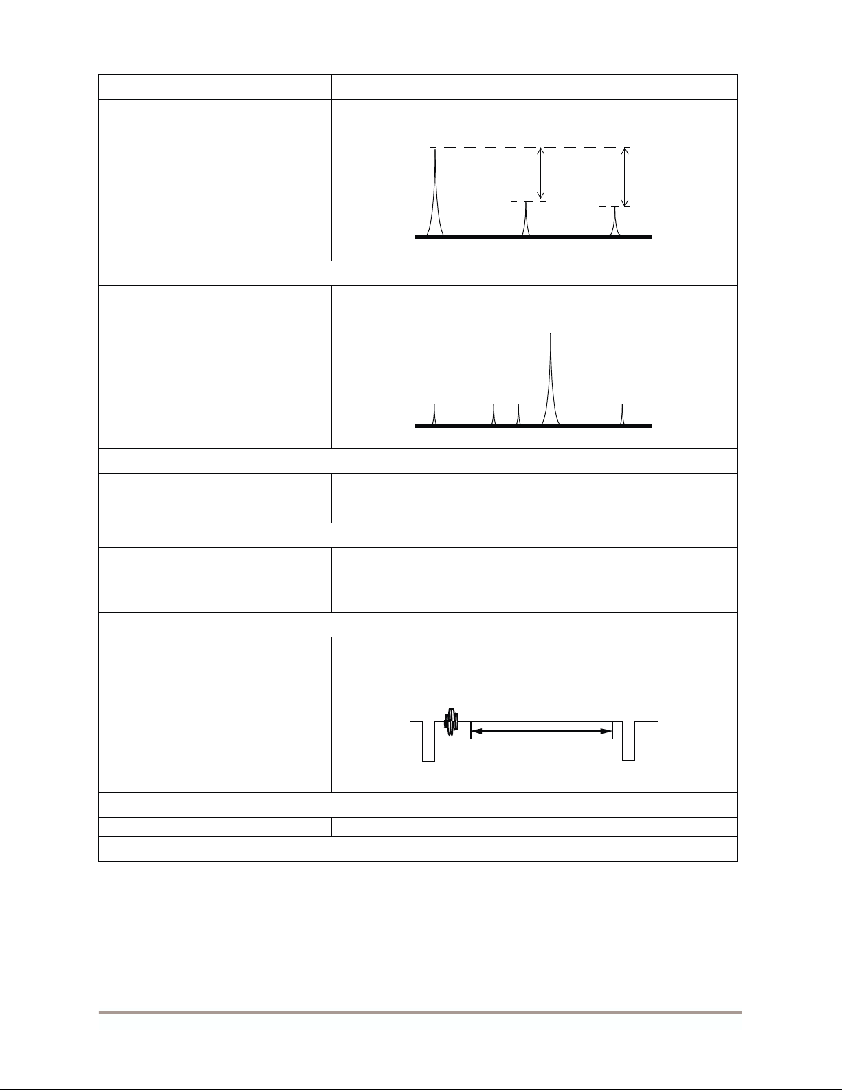
Sound Subcarrier Harmonics
Measure in dBc second and third sound harmonics levels in reference to
picture carrier (TVout_Ref).
Picture carrier
Sound carrier
+5.5MhzFo +11Mhz +16.5Mhz
Second Harmonics of Chroma subcarrier
Measure in dBc, in reference to picture carrier (TVout_Ref), second
harmonic of chroma at channel frequency plus 2 times chroma
frequency, resulting in the following spectrum.
Picture carrier
Chroma
carrier
Chroma/Sound intermodulation
Measure in dBc, in reference to picture carrier (TVout_Ref),
intermodulation product at channel frequency plus the sound carrier
frequency (+5,5Mhz) minus the chroma frequency (-4,43Mhz), resulting
in the following spectrum.
Intermodulation product is at the channel frequency +1,07Mhz.
Picture carrier
Chroma/Sound
Intermod.
Sound
2nd harm
Chroma
carrier
Sound
carrier
Chroma 2nd
Harmonic
Sound
3rd harm
+8.86MhzFo +4.43Mhz +5.5Mhz
Sound
carrier
+1.07Mhz
Fo
Picture Carrier Harmonics
8 MC44BC375/U/J/T Technical Data MOTOROLA
+4.43Mhz +5.5Mhz
For More Information On This Product,
Go to: www.freescale.com
Freescale Semiconductor, Inc.
Device and Signals Set-up Measurement Set-up
No Video signal
No Audio signal
No Video signal
No Audio signal
nc...
I
Characterization Measurement Conditions
Measure in dBc, in reference to picture carrier (TVout_Ref), second and
third harmonic of channel frequency, resulting in the following spectrum.
Picture carrier
2nd harmonic
Out of Band Spurious
Measure in dBuV spurious levels at 0.25, 0.5, 0.75 and 1.5 times channel
frequency, resulting in the following spectrum
Measure from 40Mhz to 1Ghz.
Picture carrier
Spurious
3rd harmonic
3FoFo 2Fo
cale Semiconductor,
Frees
In Band Spurious / 4Mhz Crystal Spurious
No Video signal
No Audio signal
No audio
Video: 600mVpk-pk sinusoidal signal
inserted on the black level of active video
area.
Video: 100% White video signal - 1Vpkpk.
No Audio signal
This is measured using a Rohde &
Schwarz AMFS Demodulator in B/G
(using a CCIR Rec. 567 weighting
network, 100kHz to 5MHz band with
sound trap and envelope detection, and
a Rohde & Schwarz UAF Video
Analyzer.
Same as above with CCIR filter disabled. Same as above.
Measure in dBc, in reference to picture carrier (TVout_Ref), spurious
levels falling into video bandwidth Fo+/-5Mhz (15.125Khz & 31.25Khz
from reference dividers and 4Mhz from crystal).
Video Bandwidth
The Video signal is demodulated on the spectrum analyzer, and the peak
level of the 100Khz signal is measured as a reference. The frequency is
then swept from 100Khz to 5Mhz, and then the difference in dBc from the
100Khz reference level is measured.
Weighted Video Signal to Noise
The Video Analyzer measures the ratio between the amplitude of the
active area of the video signal (700mV) and the noise level in Vrms on a
video black level which is show below.
VideoS/N is calculated as 20 x log(700 /N) in dB
Unweighted Video Signal to Noise
Video Differential Phase
Fo*3/4 Fo
N
noise level in Vrms
Fo*3/2Fo/2Fo/4
MOTOROLA MC44BC375/U/J/T Technical Data 9
For More Information On This Product,
Go to: www.freescale.com

Characterization Measurement Conditions
Device and Signals Set-up Measurement Set-up
Video: 5 step Grey Scale- 1Vpk-pk.
No Audio signal
This is measured using a Rohde &
Schwarz AMFS Demodulator in B/G
(using a CCIR Rec. 567 weighting
network, 100kHz to 5MHz band with
sound trap, and envelope detection, and
a Rohde & Schwarz UAF Video
Analyzer.
Video: 5 step Grey Scale- 1Vpk-pk.
No Audio signal
This is measured using a Rohde &
nc...
I
Schwarz AMFS Demodulator in B/G
(using a CCIR Rec. 567 weighting
network, 100kHz to 5MHz band with
sound trap and envelope detection, and
a Rohde & Schwarz UAF Video
Analyzer.
Freescale Semiconductor, Inc.
On line CCIR 330, the video analyzer DP measure consists of calculating
the difference of the Chroma phase at the black level and the different
chroma subcarrier phase angles at each step of the greyscale. The
largest positive or negative difference indicates the distortion.
DIFF PHASE = * 100%
The video analyzer method takes the worst step from the first 4 steps.
Video Differential Gain
On line CCIR 330 shown below, the video analyzer DG measure consists
of calculating the difference of the Chroma amplitude at the black level
and the different amplitudes at each step of the greyscale. The largest
positive or negative difference indicates the distortion.
the largest positive or negative difference
the phase at position 0
234
5
1
5-step Greyscale with Chroma subcarrier superimposed
0
(not to scale), line CCIR 330.
cale Semiconductor,
Frees
No Audio signal
Video:10stepgreyscale
No Video signal
No Audio Signal
“PS” bit set to 0 and 1
DIFF GAIN =*100%
The video analyzer method takes the worst step from the first 4 steps.
CCIRline330correspondstoFCCline17inNTSC/Mstandard
Video Modulation Depth
This is measured using a HP8596E Spectrum Analyzer with a TV Trigger
option, allowing demodulation and triggering on any specified TV Line.
The analyzer is centred on the maximum peak of the Video signal and
reduced to zero Hertz span in Linear mode to demodulate the Video
carrier.
TV Line Demodulated by Spectrum Analyzer-BG standard
The Modulation Depth is calculated as (A-B)/A x 100 in%
Picture to Sound ratio
Measure in dBc sound carrier in reference to picture carrier (TVout_Ref)
for “PS” bit=0 (PS=12dB typical) and for “PS” bit=1 (PS=16dB),
the largest positive or negative difference
the amplitude at position 0
A ( 6-10mV)
A(mV)
B(mV)
B (0.6 - 3mV)
Picture carrier
Sound carrier
+5.5MhzFo
Audio Modulation Depth - FM Modulation
10 MC44BC375/U/J/T Technical Data MOTOROLA
For More Information On This Product,
Go to: www.freescale.com

Freescale Semiconductor, Inc.
Device and Signals Set-up Measurement Set-up
Video Black Level
Audio signal: 1Khz, 205mVrms.
This is measured using a Rohde &
Schwarz AMFS Demodulator in B/G and
a HP8903A Audio Analyzer at 1kHz
Video Black Level
Audio signal: 50Hz to 15KHz, 100mV
This is measured using a Rohde &
Schwarz AMFS Demodulator in B/G and
a HP8903A.
nc...
I
cale Semiconductor,
Audio: 1Khz, adjustable level
Video Black Level
This is measured using a Rohde &
Schwarz AMFS UHF Demodulator in B/G
and a HP8903A Audio Analyzer at 1kHz.
The output level of the Audio analyzer is
varied to obtain a deviation of 50kHz
indicated on the Demodulator.
Audio: 1Khz, adjustable level
Video: EBU Color Bars
This is measured using a Rohde &
Schwarz AMFS Demodulator in B/G and
a HP8903A Audio Analyzer at 1kHz. The
output level of the Audio analyzer is
varied to obtain a Modulation Deviation
of 25kHz indicated on the AMFS
Demodulator.
Modulator Functionality
The audio signal 205mV at 1kHz is supplied by the Audio Analyzer, and
the FM demodulated signal deviation is indicated on the Demodulator in
Khz peak.
This value is then converted in% of FM deviation, based on specified
standards.
Audio Frequency response
The audio signal 1KHz 100mV
demodulated by the Demodulator and the audio analyzer measures the
AC amplitude of this demodulated audio signal: this value is taken as a
rms
reference (0dB).
The audio signal is then swept from 50Hz to 15KHz, and demodulated
AC amplitude is measured in dB relative to the 1KHz reference.
Audio pre-emphasis and de-emphasis circuits are engaged, all audio
analyzer filters are switched OFF.
Audio Distortion FM
The input rms detector of the Audio Analyzer converts the ac level of the
combined signal + noise + distortion to dc. It then removes the
fundamental signal (1kHz) after having measured the frequency. The
output rms detector converts the residual noise + distortion to dc. The dc
voltmeter measures both dc signals and calculates the ratio in% of the
two signals.
ADist Distorsion Noise+()Distorsion Noise Signal++()⁄=
AudioSignaltoNoise
The Audio Analyzer alternately turns ON and OFF it's internal audio
source to make a measure of the Audio signal plus noise and then
another measure of only the noise.
The measurement is made using the internal CCIR468-2 Filter of the
Audio Analyzer together with the internal 30+/-2kHz (60dB/decade)
Lowpass filters.
The AMFS demodulator uses a quasi-parallel demodulation as is the
case in a normal TV set. In this mode the Nyquist filter is bypassed and
the video carrier is used without added delay to effectuate intercarrier
conversion. In this mode the phase noise information fully cancels out
and the true S/N can be measured
is supplied by the Audio Analyzer,
rms
Frees
ASN dB() 20 Signal Noise+()Noise()⁄log×=
12 Modulator Functionality
12.1 Power Supply
The two device Vccs (pins 11 and 14) must be applied at the same time to ensure all internal blocks are
correctly biased. All other pins must not be biased before Vcc is applied to device.
MOTOROLA MC44BC375/U/J/T Technical Data 11
For More Information On This Product,
Go to: www.freescale.com

Modulator Functionality
Freescale Semiconductor, Inc.
12.2 Test modes
The MC44BC375U/J/T test modes are enabled by any voltage level higher than Vcc on pins CHS, PSS,
SFS and VIDEO. Care must be taken in the application to not reach levels higher than Vcc on those pins.
12.3 Standby modes
During standby mode, the modulator is switched to low power consumption: the sound oscillator, UHF
oscillator and VHF dividers, video and sound modulator sections bias are internally turned OFF.
Modulator is programmed in standby mode when pin 9 PSave/LO is set to “LO” level (See PIN
SELECTION section).
12.4 Logic Output Port
The Logic Output Port i s used to control an external switch (such as an antenna switch or an attenuator).
This pin is an open collector transistor able to drive up to 15mA at low voltage.
nc...
I
cale Semiconductor,
Frees
LOP level is switched between “HI” and “LO” level with pin 9 “Psave/LO” (See PIN SELECTION
section).
12.5 Transient Output Inhibit
To minimize the risk of interference to other channels while the UHF PLL is acquiring a lock on the
desired frequency, the Sound and Video modulators are turned OFF at power-ON from zero (i.e. Vcc is
switched from 0V to 5V or device is switched from “Standby mode” to “Normal operation”).
There is a time-out of 263ms until the output is enabled. This lets the UHF PLL settle to its programmed
frequency. During the 263ms time-out, the sound PLL current source is set to 10µA typicalto speed up the
locking time; after the 263ms time-out, the current source is switched to 1µA. Use care when selecting
loop filter components, to ensure the loop transient does not exceed this delay.
For test purposes, it is possible to disable the 263ms delay (see TEST MODES section).
12.6 Video section
The modulator requires a composite video input with negative going sync pulses and a nominal level of
1Vp-p. This signal is AC coupled to the video input where the sync tip level is clamped.
Video modulation depth typical value is given for 1V
value by simply adding a resistive divider at video input, resulting in a lower signal seen by the video input
stage.
input level. It can be adjusted to any lower
CBVS
The video signal is then passed to a peak white clip circuit whose function is to soft clip the top of the
video waveform if the amplitude from the sync tip to peak white goes too high. In this way overmodulation of the carrier by the video is avoided. The clipping function is always engaged.
12.7 Sound section
The multivibrator oscillator is fully integrated and does not require any external component. An internal
low pass filter and matched structure give very low harmonics level.
The sound modulator system consists of an FM modulator incorporating the sound subcarrier oscillator.
The audio input signal is AC coupled into the amplifier which then drives the modulator.
12 MC44BC375/U/J/T Technical Data MOTOROLA
For More Information On This Product,
Go to: www.freescale.com

Freescale Semiconductor, Inc.
The audio pre-emphasis circuit is a high-pass filter with an external capacitor C1 and an internal resistor
(100 kOhms t ypical). The recommended capacitor value (750pF) is f or M/N standards; time constant is
75µs. It is 470pF for B/G standards (50µs).
Audio bandwidth specification is for 50Hz to 15Khz range, with pre-emphasis circuit engaged. Without
this pre-emphasis circuit, it is possible to extend the audio bandwidth to the high frequencies as there is no
internal frequency limitation (stereo application).
Modulator Functionality
12.8 PLL Section — Dividers
The reference divider is a fixed divide by 128 resulting in a reference frequency of 31.25Khz with a
4.0Mhz crystal. The 31.25Khz reference frequency is used for both UHF and Sound PLLs.
The prescaler is a fixed divide by 8 and is permanently e ngaged. The VHF divider is different for each of
the 3 versions.
The programmable divider’s division ratio is controlled by CHS pin voltage in order to get the following
VHF frequencies:
nc...
I
cale Semiconductor,
Frees
Device Channel VHF divider
MC44BC375U
MC44BC375J
MC44BC375T CH13 = 211.25Mhz 3
12.9 Selectable Pins
Pins CHS, PSS, SFS are internally pulled up to 5V.
CH3 = 61.25Mhz
CH4 = 67.25Mhz
CH1 = 91.25Mhz
CH2 = 97.25Mhz
8
6
MOTOROLA MC44BC375/U/J/T Technical Data 13
For More Information On This Product,
Go to: www.freescale.com

Pin Circuit Schematics
Freescale Semiconductor, Inc.
13 Pin Circuit Schematics
VCC
nc...
I
cale Semiconductor,
Frees
XTAL
PREM
CHS
PSS
SFS
Psave
VCC
SPLLFLT
PLLFLT
VCC
VCC
100K
5K
11. 8k
VCC
2K
1.5K
VCC
5K
VCC
100
10k
audio
10K
VCC
75
50k
TV OUT
VCC
500
10K
VCC
VCC
LOP
VCC
TVOVCC
VIDEO
AUDIO IN
Figure 3. Pin Schematics
14 MC44BC375/U/J/T Technical Data MOTOROLA
For More Information On This Product,
Go to: www.freescale.com
Freescale Semiconductor, Inc.
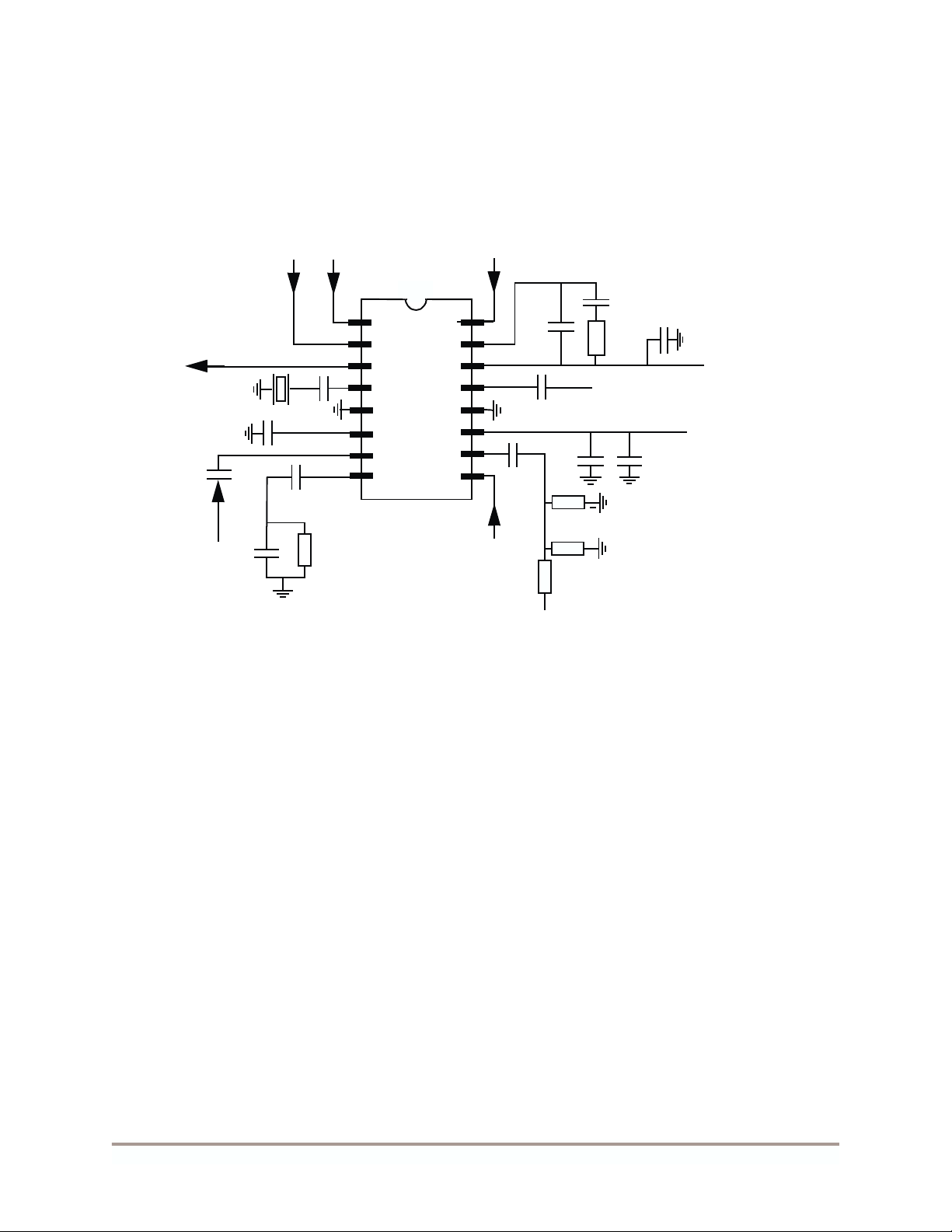
MC44BC375U Application Schematic
14 MC44BC375U Application Schematic
This document contains information
on a new product under development
Motorola reserves the right to change
or discontinue this product without notice
nc...
I
cale Semiconductor,
Frees
PS1/2
Select
LOP
O
4MHz
Pre-em
100nF
Audio
O
*: This 75
R1 and R2 are to reduce video modulation depth from typical value
Cx is dependant on the crystal characteristics (Cx=27pF on Motorola application Board)
C1 value depends on standard: 470pF is for 50µs pre-emphasis time constant (B/G standard)
and 750pF is for 75µs (M/N standard).
Ω is to match with a 75Ω video signal applied thru coaxial cable.
It can be removed in case of high impedance video generator.
(for example R1=1K
C1
22nF
CH 3/4
Select
O
O
1
2
Cx***
330nF
10k
Ω and R2=10KΩ reduce VMD by about 8%)
Figure 4. MC44BC375U Application Schematic
3
4
5
6
7
8
Psave/LO
SFS
Select
O
16
15
14
13
12
11
10
9
Loop Filter must
be as close as
22nF
1nF
10nF
O
R2**
R1**
O
Video
75*
47nF
2.2k
O
TVOUT
1nF
10nF
220nF
Vcc
O
Vcc
O
MOTOROLA MC44BC375/U/J/T Technical Data 15
For More Information On This Product,
Go to: www.freescale.com
Markings and Case Diagrams
Freescale Semiconductor, Inc.
15 Markings and Case Diagrams
15.1 Pin Description
N° Symbol Pin description Functionality
Channel 3 / Channel 4 selection for MC44BC375U
1 CHS Channel Select
2 PSS Picture to Sound Select PS=14dB / PS=16dB selection
3 LOP Logic Output Port
4 XTAL Crystal Crystal Oscillator input
5 Gnd Ground
6 PREEM Pre-emphasis Audio Pre-emphasis capacitor
7 AUDIO Audio Input
8 SPLFLT Sound PLL Filter
nc...
I
9 PSave/LO PowerSave & Logic Output control
10 VIDEO Video Input
11 VCCA Voltage supply
12 GND Ground
13 TVOUT TV Output Modulated signal Output
14 TVOVCC Voltage supply
15 PLLFLT PLL Filter UHF PLL Filter
16 SFS Sound Frequency Select Sound frequency 4.5Mhz / 5.5Mhz selection
cale Semiconductor,
Channel 1 / Channel 2 selection for MC44BC375J
Don’t care for the MC44BC375T
Logic Output Level (Low voltage / high impedance)
selectable via Pin 9
Normal Mode / Power save mode selection
In Power Save Mode, the LOP pin is automatically
switched to low voltage
Frees
16 MC44BC375/U/J/T Technical Data MOTOROLA
For More Information On This Product,
Go to: www.freescale.com
Freescale Semiconductor, Inc.
Markings and Case Diagrams
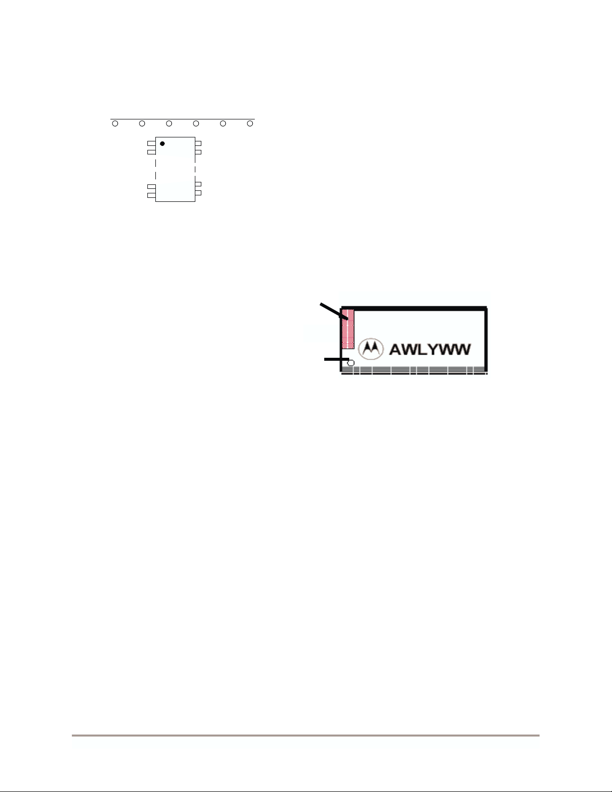
15.2 Packaging Instructions
Tape and reel packaging per 12MRH00360A with the f ollowing conditions applicable for Dual In-Line
SOP (SOIC) package.
Component Orientation: Arrange parts with the pin 1
side closest to the tape's round sprocket holes on the
tape's trailing edge.
15.3 Marking Instructions
nc...
I
cale Semiconductor,
Frees
In accordance with 12MRH00191A internal specification applied for Dual in-line SO package.
Bar marked part way accross Pin 1 end of package.
Bar width 10 to 20 mils, length to be at least four
times Bar width. Bar placement may extend across
chamfer and dimple areas.
Pin 1 Dot or Dimple
•1stline:
MC44BC375U for MC44BC375UD device
MC44BC375J for MC44BC375JD device
MC44BC375T for MC44BC375TD device
(Part number coded on 10 digits)
• 2nd line:
Assembly site code AW (2 digits) followed by the
wafer lot code L (1 digit),
year Y (1 digit) and
work week WW (2 digits)
MC44BC375x
MOTOROLA MC44BC375/U/J/T Technical Data 17
For More Information On This Product,
Go to: www.freescale.com
Markings and Case Diagrams
nc...
I
Freescale Semiconductor, Inc.
cale Semiconductor,
Frees
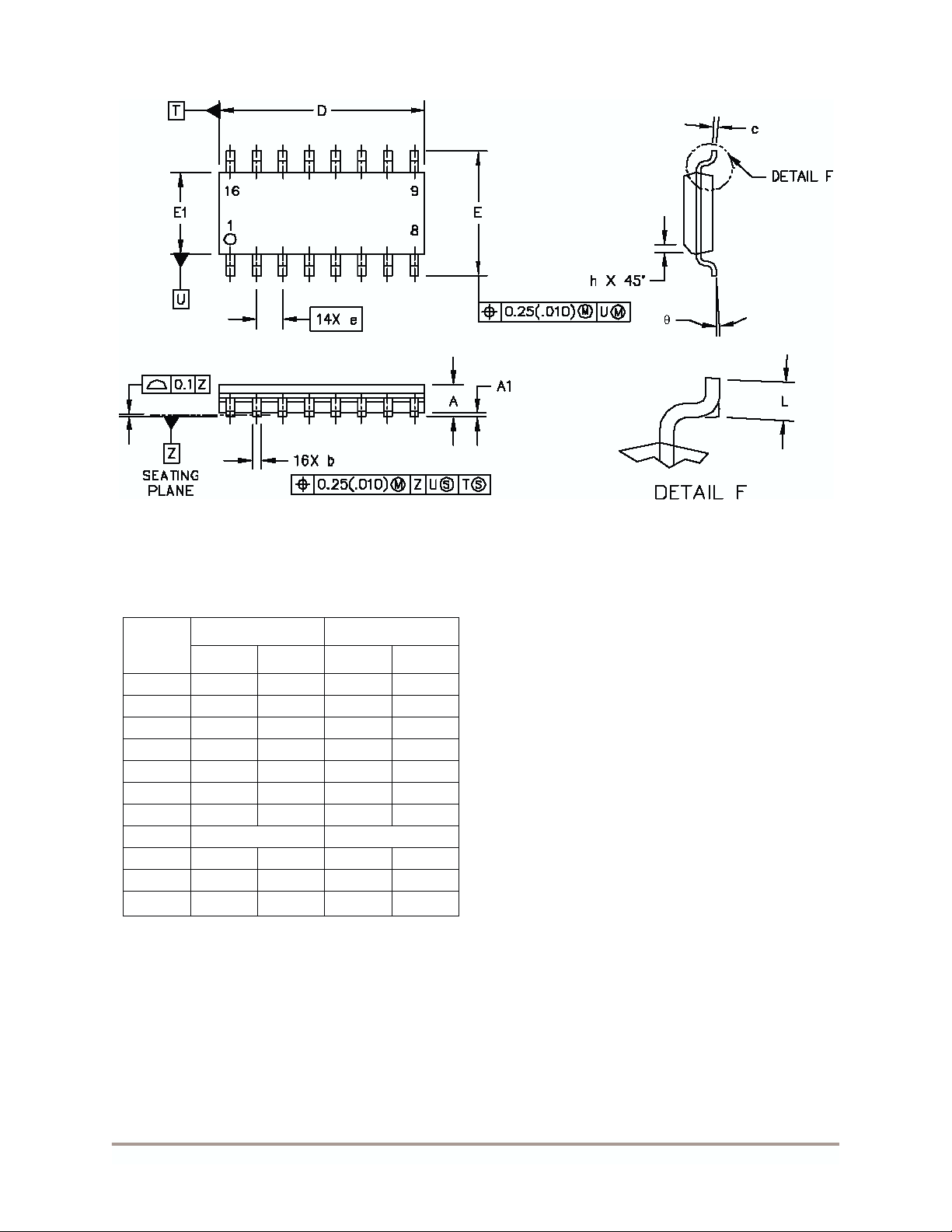
Dim
A 1.35 1.75 0.054 0.068
A1 0.1 0.25 0.004 0.009
D 9.8 10 0.385 0.393
E 5.8 6.2 0.229 0.244
E1 3.8 4 0.150 0.157
b 0.35 0.49 0.014 0.019
c 0.19 0.25 0.008 0.009
e 1.27 BSC 0.050 BSC
L 0.4 1.25 0.016 0.049
h 0.25 0.5 0.010 0.019
Q
Millimeters Inches
Min Max Min Max
o
0
o
7
o
0
Figure 5. SO16NB Package
7
Note: 1. Dimensions and Tolerances per ASME
Y14.5M, 1994.
Note: 2. Controlling dimension: Millimeters.
Note: 3.DimensionDandE1donotincludemold
protrusion.
Note: 4. Maximum mold protrusion 0.15 (0.006) per
side.
Note: 5. Dimension b does not include Dambar
protrusion.
Allowable Dambar protrusion shall be 0.127 (0.005)
total in excess of the b dimension at maximum material
condition.
o
18 MC44BC375/U/J/T Technical Data MOTOROLA
For More Information On This Product,
Go to: www.freescale.com

Freescale Semiconductor, Inc.
nc...
I
Markings and Case Diagrams
cale Semiconductor,
Frees
MOTOROLA MC44BC375/U/J/T Technical Data 19
For More Information On This Product,
Go to: www.freescale.com

nc...
I
HOW TO REACH US:
USA/EUROPE/LOCATIONS NOT LISTED:
Motorola Literature Distribution;
P.O. Box 5405, Denver, Colorado 80217
1-303-675-2140 or 1-800-441-2447
JAPAN:
Motorola Japan Ltd.; SPS, Technical Information Center,
3-20-1, Minami-Azabu Minato-ku, Tokyo 106-8573 Japan
81-3-3440-3569
ASIA/PACIFIC:
Motorola Semiconductors H.K. Ltd.; Silicon Harbour
Centre, 2 Dai King Street, Tai Po Industrial Estate,
Tai Po, N.T., Hong Kong
852-26668334
cale Semiconductor,
TECHNICAL INFORMATION CENTER:
1-800-521-6274
HOME PAGE:
Frees
http://www.motorola.com/semiconductors
Freescale Semiconductor, Inc.
Information in this document is provided solely to enable system and software implementers to
use Motorola products. There are no express or implied copyright licenses granted hereunder to
design or fabricate any integrated circuits or integrated circuits based on the information in this
document.
Motorola reserves the right to make changes without further notice to any products herein.
Motorola makes no warranty, representation or guarantee regarding the suitability of its products
for any particular purpose, nor does Motorola assume any liability arising out of the application or
use of any product or circuit, and specifically disclaims any and all liability, including without
limitation consequential or incidental damages. “Typical” parameters which may be provided in
Motorola data sheets and/or specifications can and do vary in different applications and actual
performance may vary over time. All operating parameters, including “Typicals” must be validated
for each customer application by customer’s technical experts. Motorola does not convey any
license under its patent rights nor the rights of others. Motorola products are not designed,
intended, or authorized for use as components in systems intended for surgical implant into the
body, or other applications intended to support or sustain life, or for any other application in which
the failure of the Motorola product could create a situation where personal injury or death may
occur. Should Buyer purchase or use Motorola products for any such unintended or unauthorized
application, Buyer shall indemnify and hold Motorola and its officers, employees, subsidiaries,
affiliates, and distributors harmless against all claims, costs, damages, and expenses, and
reasonable attorney fees arising out of, directly or indirectly, any claim of personal injury or death
associated with such unintended or unauthorized use, even if such claim alleges that Motorola
was negligent regarding the design or manufacture of the part.
Motorola and the Stylized M Logo are registered inthe U.S. Patent and Trademark Office. All other
product or service names are the property of their respective owners. Motorola, Inc. is an Equal
Opportunity/Affirmative Action Employer.
© Motorola, Inc. 2002
MC44BC375/D
For More Information On This Product,
Go to: www.freescale.com
 Loading...