

Page 1
查询MC44BC373供应商
Technical Data
MC44BC373/374
Rev. 3.5, 7/2003
Freescale Semiconductor, Inc.
MC44BC373/374
Multi-Standard or PAL/
NTSC Modulator with
integrated antenna
booster/splitter ICs
nc...
I
Contents
1 Features . . . . . . . . . . . . . 2
2 Device Overview . . . . . . 3
3 Maximum Ratings . . . . . 5
4 Electrostatic Discharge 5
5Electrical
Characteristics 5
2
6I
C Bit Mapping . . . . . . . 6
2
7I
C Programming . . . . . 7
8 Modulator High
Frequency
cale Semiconductor,
Frees
Characteristics 9
9 Video Characteristics . 10
10 Audio Characteristics . 11
11 Antenna Booster/Splitter
Characteristics 12
12 Modulator Operation . 14
13 High-Speed I
Compatible Bus 18
14 Application and
Case Diagrams 21
2
MC44BC373/374
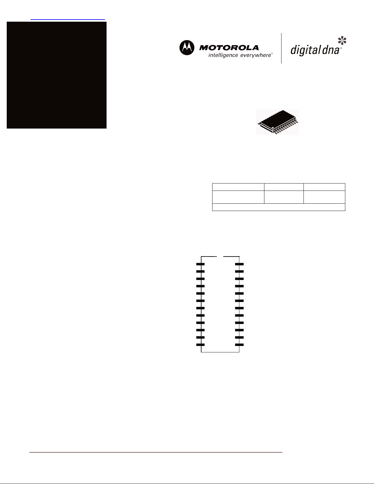
TSSOP 24 Package
Ordering Information
Device Temp Range Package
MC44BC373DTB,R2
MC44BC374DTB,R2
NOTE: For tape and reel, add R2 suffix.
These modulator ICs are for use in VCRs, games, set-top boxes, and similar devices.
Figure 1 shows the pin connections.
SCL
SDA
LOP
XTAL
GND
ANT1
ANT2
GND
PREEM
C
AUDIO
SPLFLT
AUXIN
1
2
3
4
5
6
7
8
9
10
11
12
24
23
22
21
20
19
18
17
16
15
14
13
GNDD
VCCD
PLLFLT
TVOVCC
TVOUT
GND
GND
VCRTU
VCRVCC
VCCA
VIDEO
VCCI
–10
o
C to +80oC
TSSOP24
Figure 1. MC44BC373/374 Pin Connections
This document contains information on a product under development. Motorola reserves the right to change or
discontinue this product without notice. © Motorola, Inc., 2003. All rights reserved.
For More Information On This Product,
Go to: www.freescale.com
Page 2

Features
Freescale Semiconductor, Inc.
1 Features
MC44BC373: Multi-Standard PAL/SECAM/NTSC with integrated booster splitter
MC44BC374: PAL/NTSC with integrated booster splitter
The channel is set by an on-chip high-speed I
the modula tor o v er th e full UHF range. The modulator incorporates a sound subcarrier oscillator and uses
a second PLL to derive 4.5, 5.5, 6.0, and 6.5MHz subcarrier frequencies. These frequencies are selected
using the bus.
The picture-to-sou nd ratio is adjus ted using the bu s. In addi tion, an on-chip v ideo test patter n generat or can
be switched ON using a 1kHz audio test signal.
Along with the modulator functions, an Antenna Booster/Splitter function is included.
These modulator versions are comple tely pin-to-pin and software compatible and all versions have the
following fe atures.
• No external varicaps diodes /inductors or tuned components
2
C compatible bus receiver. A Phase-Locked Loop (PLL) tunes
nc...
I
cale Semiconductor,
Frees
• Channel 21–69 UHF operation
• VHF range possible by internal dividers (30MHz to 450MHz)
• Integrated on-chip programmable UHF oscillator
• Extremely low external component count
2
• High-speed read and write I
• Fixed video modulation depth (80% in PAL and 90% in SECAM)
• Peak White Clip disabled using the bus
• Programmable picture/sound carrier ratio (12dB and 16dB)
• Integrated on-chip programmable sound subcarrier oscillator
(4.5MHz to 6.5MHz)—No external varicaps
• On-chip video test pattern generator with sound test signal (1kHz)
• Low-power programmable modulator standby mode
(booster active)
• Transient output inhibit during PLL Lock-up at Power-ON
• Logical Output Port controlled by bus
• Integrated Antenna Booster/Splitter (40MHz to 860MHz)
• Custom masked versions with unique start-up settings possible
2
C bus programming required)
(no I
C-bus compatible (800kHz)
• Extremely robust ESD protection, minimum 4kV, typical 6kV
2 MC44BC373/374 Technical Data MOTOROLA
For More Information On This Product,
Go to: www.freescale.com
Page 3

Freescale Semiconductor, Inc.
2 Device Overview
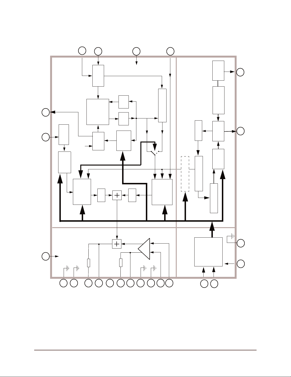
Figure 2 shows a simplified block diagram of the MC44BC373/4 device.
The MC44BC373/374 device contains four main sections:
Device Overview
1. A high-speed I
2. A PLL section — Synthesizes the UHF/VHF output channel frequency (from an integrat ed
UHF oscillator, divided for VHF output).
3. A modulator section — Accepts audio and video inputs and then uses those inputs to
modulate the UHF/VHF carrier.
4. An Antenna Booster/Splitter — Am plifies and splits the antenna signal into two signals:
a) The modulated signal is added to the amplified antenna signal on the TVOUT pin.
a)
The following items are programmable using the high-speed I
nc...
I
cale Semiconductor,
• Channel frequency
• Sound frequency
• Sound/picture carrier ratio
An on-chip video test pattern generator with an audio test signal is included.
The MC44BC373 operates as a multi-standard modulator and can handle the following systems using the
same external circuit components:
•B/G
•I
•D/K
•H
•L
•M/N
The high frequency BiCMOS technology permits integration of the following functions:
• Antenna Booster/Splitter
• UHF tank circuit and certain filtering
2
C-compatible bus section.
2
C compatible bus:
Frees
MOTOROLA MC44BC373/374 Technical Data 3
For More Information On This Product,
Go to: www.freescale.com
Page 4
Device Overview
Freescale Semiconductor, Inc.
nc...
I
cale Semiconductor,
Frees
11
14
3
LOP VIDEO SPLLFLT
AUDIO
10
SECTION
MODULATOR
Clamp
kHz
31.25
Peak
White
L/BG
Video
C BUS
2
I
BST
SECTION
Modulator
Ω
75
Sound
PREEM
9
Audio
Amplifier
and FM
Oscillator
PFD
Sound
L/BG
Modulator
Prog
LPF
I2C BUS
Ω
75
ALCLPF
Divider
2
C BUS
I
LPF
VCCA
15
FM
4dB
L/BG
AM Modulator
AM
Sound
AUX IN
12
31.25kHz
C BUS
I
4
22
23 24
XTALPLLFLTGNDDVCCD
XCO
4MHz
/128
Ref Divider
VCO and PLL SECTION
PLL
UHF OSC
VHF Dividers
Modulator
2
I
C BUS
BUS SECTION
High-Speed
Comp
Phase
Prog
Divider
2
Prescaler/ 8
C Bus
2
I
Receiver
6
5
GND
8
GND
21
19
18
GND
GND
Figure 2. Simplified Block Diagram—MC44BC373 / 374
4 MC44BC373/374 Technical Data MOTOROLA
20
13
VCCI
TVOUT
TVOVCC
For More Information On This Product,
Go to: www.freescale.com
16
17
VCRTU
7
ANT2
ANT1
1
2
SCL
SDA
Page 5
Freescale Semiconductor, Inc.
Maximum Ratings
3 Maximum Ratings
Sym Parameter Value Unit
Vcc1 Supply Voltage 6 V
Tamin Minimum Operating Ambient Temperature –10
Tamax Maximum Operating Ambient Temperature 75
Tstgmin Minimum Storage Temperature –65
Tstgmax Maximum Storage Temperature 150
o
o
o
o
This device contains protection circuitry to
guard against damage due to high static
voltage or electric fields. However, precautions
must be taken to avoid applications of any
C
voltage higher than maximum rated voltages to
this high impedance circuit. For proper
C
operation, input and output voltages should be
constrained to the ranges indicated in the
C
Recommended Operating Conditions.
C
Maximum ratings are those values beyond which damage to the device may occur. For functional
operation, voltage should be restricted to the Recommended Operating Condition.
4 Electrostatic Discharge
nc...
I
cale Semiconductor,
Frees
Sym Parameter Min Typ Unit
ESD HBM (Human Body Model)—MIL-STD-883C, Method 3015-7 4000 6000 V
5 Electrical Characteristics
• A = 100% Tested
• B = 100% Correlation tested
• C = Characterized on samples
• D = Design parameter
5.1 Specification Conditions
Unless otherwise stated: Vcc=5.0V, Ambient Temperature=25oC, Video Input 1V
grayscale. RF inputs/outputs into 75Ohm load. SPECIFICATIONS ONLY VALID FOR ENVELOPE
DEMODULATION.
Parameter Min Typ Max Unit Notes Type
Operating supply voltage range 4.55.05.5V B
Total supply current 65 75 88 All sections active A
Total standby mode supply current 26 34 40 mA
Test pattern sync pulse width 3 4.76.5 µSB
Sound comparator charge pump current
During locking
When locked
RF comparator charge pump current 60 100 150 µAA
Crystal oscillator stability-negative resistance 1 ——KΩ D
Logic Output Port
Saturation voltage at I=2 mA
Leakage current
7
10112
0.7
——160—3001mV
1.5µAµA
OSC, SO, ATT= 1
Bus Section active
µA
, 10-step
p-p
A
A
A
A
A
MOTOROLA MC44BC373/374 Technical Data 5
For More Information On This Product,
Go to: www.freescale.com
Page 6
2
I
C Bit Mapping
Freescale Semiconductor, Inc.
6 I2C Bit Mapping
WRITE MODE Bit 7 Bit 6 Bit 5 Bit 4 Bit 3 Bit 2 Bit 1 Bit 0 ACK
CA-CHIP ADDRESS 11001010ACK
C1-High Order Bits 1 AUX SO LOP PS X3 X2 SYSL ACK
C0-Low Order Bits PWC OSC ATT SFD1 SFD0 TB1 X5 X4 ACK
FM-High Order Bits 0 TPEN N11 N10 N9 N8 N7 N6 ACK
FL-Low Order Bits N5 N4 N3 N2 N1 N0 X1 X0 ACK
READ MODE Bit 7Bit 6Bit 5Bit 4Bit 3Bit 2Bit 1Bit 0ACK
CHIP ADDRESS 11001011ACK
R-Status Byte —————Y2 Y1 OOR —
Bit Name Description
PWC Peak White Clip enable / disable.
OSC UHF oscillator ON/OFF.
nc...
I
cale Semiconductor,
ATT Modulator output attenuated-sound and video modulators ON/OFF.
SFD0, 1 Sound subcarrier frequency control bits.
TB1 Test mode bit—bus format compatible with MC44353.
AUX Auxiliary sound input enable/disable.
SO Sound Oscillator ON/OFF.
LOP Logic Output Port.
PS Picture-to-Sound carrier ratio.
SYSL System L enable—selects AM sound and positive video modulation ( MC44BC373/ only).
TPEN Test pattern enable—picture and sound.
X5…X0 Test mode bits—All bits are 0 for normal operation (see Test Mode tables, page 7 & page 8).
N0…N11 UHF frequency programming bits, in steps of 250kHz.
OOR RF oscillator out-of-frequency range information.
Y1, Y2 RF oscillator operating range information.
Frees
6 MC44BC373/374 Technical Data MOTOROLA
For More Information On This Product,
Go to: www.freescale.com
Page 7
Freescale Semiconductor, Inc.
7 I2C Programming
I2C Programming
nc...
I
cale Semiconductor,
Frees
Sound
SFD1 SFD0 Sound Subcarrier Freq (MHz)
00 4.5
01 5.5
10 6.0
11 6.5
PS Picture-to-Sound Ratio (dB)
012
116
UHF
OSC UHF Oscillator
0 Normal operation.
UHF oscillator disabled ( oscillator and PLL
1
sections bias turned OFF ).
ATT Modulator Output Attenuation
0 Normal operation.
Modulator output attenuation (sound and
1
video modulators sections bias turned OFF ).
Standby Mode
SO Sound Oscillator
0 Sound oscillator ON (normal mode).
Sound oscillation disabled (oscillator and PLL
1
section bias turned OFF).
AUX Auxiliary Audio Input
0 AUX input disabled (normal mode).
1 AUX input enabled.
OSC SO ATT Combination of 3-bits
111
MC44353/4/5 Compatibility
Video
TB1 Description
SYSL
System B/ G enabled, System L disabled
0
(FM sound and negative video modulation).
System L enabled, System B / G disabled
1
(AM sound and positive video modulation).
PWC Peak White Clip
0 Peak White Clip ON (System B/G).
1 Peak White Clip OFF (System L).
TPEN Test Pattern Signal
0 Test pattern signal OFF (normal operation).
System L and B/ G Selection
MC44BC373 only
0 Normal mode (fully programmable).
Limited programmability and compatibility with
1
MC44353.
Logic Output Port
LOP Description
0 Pin 3 is low voltage.
1 Pin 3 is high impedance.
WRITE MODE: Test Mode 1 and VHF Range
X2 X1 X0 State Description
Modulator standby mode (sound
and UHF oscillator, sound and
video modulator section bias
turned OFF, and I
standby mode)—BST is active.
2
C bus section
0001.a Normal operation.
0011.b RF frequency divided for low frequency testing or VHF range: RF/ 2
0101.cRF/4
0111.dRF/8
1001.eRF/16
1011.f DC drive applied to modulators: non-inverted video at TVOUT.
1101.g DC drive applied to modulators: inverted video at TVOUT.
1111.h Transient output inhibit disabled.
MOTOROLA MC44BC373/374 Technical Data 7
For More Information On This Product,
Go to: www.freescale.com
Page 8
2
I
C Programming
Freescale Semiconductor, Inc.
WRITE MODE: Test Mode 2
X5 X4 X3 State Description
0002.a Normal operation.
0012.b Test pattern generator DC verification (Test pattern DC test mode available).
0102.c
0112.d Reference divider test (UHF reference divider on PLLFILT pin).
1002.e
1012.f
1102.g
nc...
I
1112.h
Programmable divider test (UHF programmable divider on PLLFILT pin and
sound programmable divider on SPLLFIL pin).
UHF phase comparator, upper source on PLLFILT pin.
Sound phase comparator 10 µA upper source on SPLLFIL
(only valid during Transient Output Inhibit).
UHF phase comparator, lower source on PLLFILT pin.
Sound phase comparator 10 µA lower source on SPLLFIL
(only valid during Transient Output Inhibit).
Sound phase comparator 1 µA upper source on SPLLFIL
(not valid during Transient Output Inhibit).
Sound phase comparator 1 µA lower source on SPLLFIL
(not valid during Transient Output Inhibit).
READ MODE
OOR Description
cale Semiconductor,
Frees
0 Normal operation, VCO in range.
1 VCO out-of-range.
Y1 Description
0 VCO out-of-range, frequency too low, only valid if OOR=1.
1 VCO out-of-range, frequency too high, only valid if OOR= 1.
Y2 Description
0 High VCO is active.
1 Low VCO is active.
8 MC44BC373/374 Technical Data MOTOROLA
For More Information On This Product,
Go to: www.freescale.com
Page 9

Freescale Semiconductor, Inc.
Modulator High Frequency Characteristics
8 Modulator High Frequency Characteristics
nc...
I
cale Semiconductor,
Frees
Unless otherwis e state d: Vcc=5.0V, Ambient Temperature=25oC, Video Input 1V
, 10-step grayscale.
p-p
RF inputs /outputs into 75Ohm load. SPECIFICATIONS VALID ONLY FOR ENVELOPE
DEMODULATION.
Parameter Test Conditions Min Typ Max Unit Type
TVOUT output level
UHF oscillator frequency — 460 — 880 MHz A
VHF range From UHF oscillator internally divided. 45 — 460 MHz B
TVOUT output attenuation
Sound subcarrier harmonics (Fp + n∗Fs) Reference picture carrier. —–63 –58 dBc C
Second harmonic of chroma subcarrier Using red EBU bar. –65 ——dBc C
Chroma/ Sound intermodulation:
Fp + (Fsnd– Fchr)
Fo (picture carrier) harmonics
Out band (picture carrier) spurious
In band spurious (Fo 5 MHz) No video sound modulation. ——60 dBc C
NOTE 1: Picture carrier harmonics are highly dependant on printed circuit board layout and decoupling capacitors.
40
35
30
dBc
25
20
15
471 521 571 621 671 721 771 821 871
78
Maximum specification
77
76
75
dBuV
74
73
72
471 521 571 621 671 721 771 821 871
2Fo Harmonics
Minimum specification
Frequency (Mhz)
TV Output Level
Minimum specification
Frequency (Mhz)
Output signal from modulator section.
See Figure 3.
During transient output inhibit, or
when ATT bit is set to 1. See Figure 3.
Using red EBU bar. –65 ——dBc C
2nd harmonic: CH21
3rd harmonic: CH21
Other channels: See Figure 3.
See NOTE 1.
1/2∗ Fo – 1/4∗ Fo – 3/2∗ Fo – 3/4∗ Fo
From 40MHz to 1GHz.
45
40
35
Typi cal
Typi cal
30
dBc
25
20
Minimum specification
15
471 521 571 621 671 721 771 821 871
75
70
65
60
dBc
55
50
45
TV Output Atte nuation
471 521 571 621 671 721 771 821 871
73 74.577dBµVB
50 60 — dBc B
30203526—
— dBc C
— 010dBµVC
3Fo Harmonics
Typ ical
Frequency (Mhz)
Typi cal
Minimum specification
Frequency (M hz)
Figure 3. Typical Performance—Modulator High Frequency
MOTOROLA MC44BC373/374 Technical Data 9
For More Information On This Product,
Go to: www.freescale.com
Page 10

Video Characteristics
Freescale Semiconductor, Inc.
9 Video Characteristics
nc...
I
cale Semiconductor,
Frees
Unless otherwis e sta te d: Vcc=5.0V, Ambient Temperature =25oC, Video Input 1V
, 10-step
p-p
grayscale. RF inputs/outputs into 75Ohm load. SPECIFICATIONS VALID ONLY FOR ENVELOPE
DEMODULATION.
Parameter Test Conditions Min Typ Max Unit Type
Video bandwidth
Video input level 75Ohm load. ——1.5VcvbsD
Video input current ——0.21µA A
Video input impedance — 500 ——KΩ A
Peak White Clip PWC bit set to 1, see PWC section. 110 114 118 % A
Video S/ N See Figure 4. 50 53 — dB C
Differential Phase See Figure 4. –5 — 5 deg C
Differential Gain
Luma/ Sync ratio Input ratio 7.0:3.06.8/3.2 — 7.2/2.8 — B
PAL video modulation depth — 75 81 88 % B
SECAM video modulation depth — 88 93 99 % B
PAL Video Modulation Depth
90
88
86
84
82
%
Typ ical
80
78
76
74
471 521 571 621 671 721 771 821 871
Frequency (Mhz)
Reference 0dB at 100 kHz,
measured at 5 MHz.
On line CCIR 310, worst of first 4 out
of 5 steps. See Figure 4.
Video Signal to Noise
58
56
54
dB
52
50
48
Maximum specification
Minimum specification
Typical
Minimum specification
471 521 571 621 671 721 771 821 871
Frequency (Mhz)
–1.5 –0.8 — dB C
–5 — 5%C
SECAM Video Modulation Depth
100
98
96
94
%
Typical
92
90
88
86
471 521 571 621 671 721 771 821 871
Maximum specification
Minimum specification
Frequency (Mhz)
Figure 4. Typical Performance—Video
10 MC44BC373/374 Technical Data MOTOROLA
For More Information On This Product,
Go to: www.freescale.com
Page 11

Freescale Semiconductor, Inc.
10 Audio Characteristics
Audio Characteristics
nc...
I
cale Semiconductor,
Frees
Unless otherwis e sta te d: Vcc=5.0V, Ambient Temperature =25oC, Video Input 1V
, 10-step
p-p
grayscale. RF inputs/outputs into 75Ohm load. SPECIFICATIONS VALID ONLY FOR ENVELOPE
DEMODULATION.
Parameter Test Conditions Min Typ Max Unit Type
Picture-to-Sound ratio
Audio modulation depth
Audio input resistance — 45 53 61 KΩ A
Audio Frequency response
Audio Distortion FM (THD only)
Audio Distortion AM (THD only)
Audio S/ N with Sync Buzz FM
Audio S/ N with Sync Buzz AM
PS bit set to 0.
PS bit set to 1.
Using specific pre-emphasis circuit,
audio input level=205 mVrms–audio frequency=1kHz
AM modulation: SECAM Fs=6.5MHz 65 80 95 % B
FM modulation: Fs=5.5, 6 or 6.5MHz
100% modulation=±50kHz FM deviation
FM modulation: NTSC Fs=4.5MHz
100% modulation=±25 kHz FM deviation
Reference 0dB at 1kHz,
using specified pre-emphasis circuit,
measure from 50Hz to 15kHz. –2.5 — +2dB C
At 1kHz, 100% modulation (± 50kHz).
No video.
At 1kHz, 100% modulation.
No video.
Video input EBU color bar 75%.
Weighting filter CCIR 468-2.
Reference 1kHz, 85% modulation.
Video input EBU color bar 75%.
Audio BW from 40Hz to 15kHz.
Weighting filter CCIR 468-2.
Audio Signal to Noise
58
56
Typical
Minimum specification
471 521 571 621 671 721 771 821 871
Frequency (Mhz)
dB
54
52
50
48
46
13
65 80 95 % B
65 80 95 % B
— 0.42 % C
— 1.52.5% D
48 53 — dB C
45 50 — dB D
16
9
12
19
15
dB B
Figure 5. Typical performance—Audio
MOTOROLA MC44BC373/374 Technical Data 11
For More Information On This Product,
Go to: www.freescale.com
Page 12

Antenna Booster/Splitter Characteristics
Freescale Semiconductor, Inc.
11 Antenna Booster/Splitter Characteristics
Unless otherw ise s tat ed: Vcc=5.0V, Ambient Temperature=25oC, RF inputs/outputs into 75Ohm load.
All specifications use a BALUN at ANT1 & 2 inputs, assuming 0.8dB losses MA X from 40MHz to
860MHz.
Parameter Test Conditions Min Typ Max Unit Type
Frequency range — 40 — 860 MHz C
Gain
Gain flatness 40 to 860MHz. –1.5 + 1.5dB C
Noise figure
Noise figure
VSWR
nc...
I
Intermodulation
(IMD)
Isolations
ANT1, 2 to VCRTU.
ANT1, 2 to TVOUT.
ANT1, 2 to VCRTU and TVOUT.
Modulator in standby mode.
ANT1, 2 to VCRTU and TVOUT.
Modulator in normal mode (ON).
All pins, BST bias ON.
At TVout and VCRTU pins, BST bias OFF.
At TVin pins, BST bias OFF. — 2.53 — B
Input level=90 dBuV. See IMD measurement section.
F1+F2 IMD
2F1–F2, 2F2+ F1, F1–F2 IMD
From TVOUT or VCR to ANT1, 2
TVOUT/VCRTU
—
5.57.59.5dB C
6.58.510.5dB C
— 1.52.5 — B
—
—
48
30
55
60
60
45
4
4
—
47
50
—
—
dB
dB
dBc
dBc
dBc
dBc
B
B
C
C
C
C
cale Semiconductor,
Frees
11.1 Typical Performance—Gain and Isolation
Gain ANT1 ,2 to VCRTU and TVOUT
7
Maximum specification
6
5
4
dB
3
2
Minimum specification
1
0 150 300 450 600 750 900
-30
-40
-50
-60
dBc
-70
-80
-90
0 150 300 450 600 750 900
Fre q u e n cy (M h z )
Isolation Output to Input
Minimum specification
Frequency (M hz)
Typical
Typ ical
Is olation Output to Output
-10
-20
Minimum specification
-30
-40
dBc
-50
-60
-70
0 150 300 450 600 750 900
Frequency (M hz)
TVOUT
VCRTU
Typical
Figure 6. Typical Performance—Gain and Isolation
12 MC44BC373/374 Technical Data MOTOROLA
For More Information On This Product,
Go to: www.freescale.com
Page 13

Freescale Semiconductor, Inc.
Antenna Booster/Splitter Characteristics
11.2 Typical Performance—Noise Figure
nc...
I
cale Semiconductor,
Frees
Noise Figure @ M odula tor OFF
11
10
9
8
dB
7
6
5
0 150 300 450 600 750 900
Maximum specification
Typ ical
Frequency (M hz)
Figure 7. Typical Performance—Noise Figure
Noise Figure @ M odulator ON
12
11
10
9
dB
8
7
6
0 150 300 450 600 750 900
Maximum specification
Typical
Frequency (M hz)
11.3 Intermodulation (IMD ) Measurement
F1
50/75
F2
BALUN
MC44BC373/4
90dBuV
F1 F2
Figure 8. Intermodulation (IMD) Measurement
Intermodulation (IMD) frequencies are all frequency combinations coming from the two input carriers F1
and F2: F2–F1, 2∗F1–F2, 2∗ F2–F1 and F1+F2, fall in the 40M Hz–900MHz range.
F1 and F2 input levels are set t o 90dBuV at the input of the BALUN. F1 and F2 frequency generator level s
(50W internal load) take into account a 50 to 75Ohm load difference (1.8dB), plus losses in the 3dB
coupler and the 50 to 75Ohm transformer.
TVOUT
Pin 20
Pin 17
VCRTU
75/50
75/50
F2–F1
Spectrum Analyzer
IMD (dBc)
F1
F2
2F1–F2
2F2–F1
F1+F2
Intermodulation measurement is the difference (in dBc) between the F1 or F2 level at the Output (VCRTU
or TVOUT) and the frequency combinations level, for the following cases:
F1= 50MHz and F2=60MHz F1= 100MHz and F2= 110MHz F1=200MHz and F2=210MHz
F1= 300MHz and F2=310MHz F1 =400MHz and F2= 410MHz F1=500MHz and F2=510MHz
F1= 600MHz and F2=610MHz F1 =700MHz and F2= 710MHz F1=800MHz and F2=810MHz
Intermodulation specification is the IMD measurement’s worst case.
MOTOROLA MC44BC373/374 Technical Data 13
For More Information On This Product,
Go to: www.freescale.com
Page 14

Modulator Operation
Freescale Semiconductor, Inc.
12 Modulator Operation
12.1 Power-ON Settings
At power-ON, the MC44BC373 and MC44BC374 configuration is as follows:
WRITE MODE Bit 7 Bit 6 Bit 5 Bit 4 Bit 3 Bit 2 Bit 1 Bit 0 ACK
C1—High Order Bits 10000000ACK
C0—Low Order Bits 00001000ACK
FM—High Order Bits 0 0 N11 N10 N9 N8 N7 N6 ACK
FL—Low Order Bits N5 N4 N3 N2 N1 N0 0 0 ACK
Note: 1. N0 to N11 are set to have the UHF oscillator on channel 36 (591.25MHz).
Note: 2. Peak White Clip is ON.
Note: 3. Sound frequency is 5.5MHz.
Note: 4. Sound auxiliary input is disabled.
nc...
I
Note: 5. Logic Output Port is low voltage.
Note: 6. Picture-to-sound ratio is 12dB.
cale Semiconductor,
Frees
The settings indicated can be customized in the special masked version.
12.2 Power Supply
The five device Vcc pins (13, 15, 16, 21, 23) must be applied at the same time to ensure al l int ernal blocks
are correctly biased. All other pins must not be biased before Vcc is applied to the device. The printed
circuit board layout of the Vcc supplies must be designed to ensure maximum is olation of the I/P to O/P
and also between the two O/Ps.
12.3 Standby Mode
During standby mode, the modulator is switched to low power consumption; the sound oscillator, UHF
oscillator, video and sound modulator sections bias are internally turned OFF.
2
The I
C bus and booster sections remain active.
The modulator can be programmed in standby mode using a combination of three bits:
1. OSC=1
2. SO=1
3. ATT=1
14 MC44BC373/374 Technical Data MOTOROLA
For More Information On This Product,
Go to: www.freescale.com
Page 15

Freescale Semiconductor, Inc.
Modulator Operation
12.4 Test Bit TB1
This test bit allows an initial evaluati on of MC44BC373 and MC44BC374 using software developed for
MC443535:
• TB1= 0 — All MC44BC373/374 functions available—normal mode.
• TB1= 1 — Limited software compatibility with MC44353; MC44BC373/374 functions not
available.
nc...
I
cale Semiconductor,
Frees
WRITE MODE
CA-CHIP ADDRESS 11001010ACK
C1-High Order Bits 1 ——PS ——SYSL ACK
C0-Low Order Bits ———SFD1 SFD0 1 0 0 ACK
FM-High Order Bits 0 TPEN N11 N10 N9 N8 N7 N6 ACK
FL-Low Order Bits N5 N4 N3 N2 N1 N0 ——ACK
Note: 1. Case TB1= 1, compatible with MC44353
Note: 2. All “—” are don’t care bits.
Note: 3. PS bit replaces PSD2 bit in MC44353 bus format:
PS = 0 is for picture-to-sound ratio = 12dB,
PS = 1 is for picture-to-sound ratio = 16dB
Note: 4. SFD1 and SFD0 bits have the same definition for both bus formats (MC44353 and MC44BC373/374) and
lets a sound frequency between 4.5MHz, 5MHz, 5.5MHz, and 6.5MHz be selected.
Note: 5. SYSL bit has same definition for bus formats MC44353 and MC44BC373/ 374; either system L or B/G is
selectable.
Note: 6. All MC44BC373/ 374 functions are set to their default values.
1
Bit 7 Bit 6 Bit 5 Bit 4 Bit 3 Bit 2 Bit 1 Bit 0 ACK
12.5 System L or B/G Selection
SYSL bit internally switches the follow ing functions :
• SYSL = 0; e nables B/G system
— Video modulation polarity—Negative
— Video modulation depth—80% Typical (See Video Characteristics on page 10.)
— Sound modulation type—FM
• SYSL = 1; enables L system
— Video modulation polarity—Positive
— Video modulation depth—90% Typical (See Video Characteristics on page 10.)
— Sound modulation type—AM
12.6 Transient Output Inhibit
To minimize the risk of interference to other channels while the UHF PLL is acquiring a lock on the
desired frequency, the Sound and Video modulators are turned OFF for each of the following two cases:
1. Power-ON from zero (i.e., all Vcc is switched from 0V to 5V).
2. UHF oscillator power-ON from OFF state (i.e., OSC bit is switched from 1 to 0)
MOTOROLA MC44BC373/374 Technical Data 15
For More Information On This Product,
Go to: www.freescale.com
Page 16

Modulator Operation
There is a time-out of 263ms until the output is enabled. This allows the UHF PLL settle to its
programmed frequency. During the 263m s time-out, the sound PLL current source is set to 10µA typical,
to speed up the locking time. After the 263ms time-out, the current source is switched to 1µA.
Use care when selecting loop filter components, to ensure the loop
transient does not exceed the specified delay.
For test purposes, it is possible to disable the 263ms delay using Test Mode1–State1.h.
Freescale Semiconductor, Inc.
CAUTION:
12.7 Logic Output Port (LOP)
The LOP pin controls any logic function. The primary applications are to control an external attenuator or
an external switch betwee n the antenna input and TV output. When an external switch is controlled, the
Booster function is not used.
The following figure shows a typical attenuator application with PIN diode. The LOP pin switc hes the
PIN attenuator depending on the signal strength of the Antenna Input, thereby reducing the risks of
nc...
I
Intermodulation in c ertain a reas. The LOP may also be use d as an OFF posit io n bypass switc h or for other
logic function s in the ap plica tion.
cale Semiconductor,
Frees
Vcc
Antenna
Input
LOP pin
Figure 9. Attenuator Application with PIN Diode
TV Out
12.8 Video Section—Peak White Clip
The modulator requires the following:
• A composite video input with “negative going” sync pulses
• A nominal level of 1Vp-p
This signal is AC-coupled to the video input where the sync tip level is clamped. The video signal is then
passed to a Pea k White Clip (PWC) circuit. The PWC circuit function sets to soft- clip the top of the video
waveform, if the “sync tip amplitude” to “peak white clip” goes too high. This method avoids carrier overmodulation by the video. Clipping can be disabled by software.
12.9 Sound Section
The multivi brator oscillator is fully integrated and does not require external components. An internal low
pass filter and matched structure provide a very low harmonics level.
The sound modulator system consists of an FM modulator incorporating the sound subcarrier oscillator,
and an AM modulator. The audio input signal is AC coupled into the amplifier which then drives the two
types of modulators.
The audio pre-emphasis circuit is a high-pass filter with an external capacitor and an internal resistor
(100kOhms). The recommended capacitor value (470pF) is for BG standard. (50µS time constant.)
16 MC44BC373/374 Technical Data MOTOROLA
For More Information On This Product,
Go to: www.freescale.com
Page 17

Freescale Semiconductor, Inc.
The auxiliary audio input adds a sound subcarrier to the main carrier. The input can be a modulated
NICAM carrier or a second sound subcarrier for a stereo system. Pin 12 is directly connected to the sound
modulator input and the pict ure-to -soun d ratio (P/S Rati o) de pends o n the auxil iary audio inp ut le vel. (P/S
ratio is 20dB for 35mVrms typical.)
Modulator Operation
12.10 Test Pattern Generator
A simple test pattern is generated on the IC which can be switched in under bus control to permit a TV
receiver to eas ily t une i n to t he mo dulat or out put. The patt ern co nsist s of t wo whit e vert ical bars on a blac k
background and a 976Hz audio test signal.
TE2
nc...
I
TE1
10 20 30 40 50 60
0
Figure 10. Test Pattern Generator—(Time in Seconds)
24 28 44
TIME IN µS.
12.11 PLL Section
The reference divider is a fixed divide-by-128, resulting in a reference frequency of 31.25KHz with a
4.0MHz crystal. The 31.25KHz referen ce fr eque ncy is used for both UHF and Sound PLLs.
The prescaler is a fixed divide by 8 and is permanently engaged.
The programmable div ide r’ s di vi sion ratio is controlled by the state of contr ol bit s N0 t o N11. The div ide r
ratio N for a desired frequency F (in MHz) is provided by the following formulas:
F
cale Semiconductor,
with:
N
128
-- -
-------- -
×=
8
7/10
3/10
64
4
Frees
N 2048 N11× 1024 N10×……4N2× 2N1× N0+ ++++=
12.12 UHF Oscillator—VHF Range
The UHF oscillator is fully integrated and does not require any external components. For low frequency
testing or VHF ra nge ope rati on (t est mod e 1, states 1.b to 1.c), the UHF oscilla tor can be inter nally divi ded
by 2, 4, 8, or 16.
MOTOROLA MC44BC373/374 Technical Data 17
For More Information On This Product,
Go to: www.freescale.com
Page 18

High-Speed I
2
C Compatible Bus
Freescale Semiconductor, Inc.
13 High-Speed I2C Compatible Bus
13.1 Specification Conditions
Unless otherwise specified, the Vcc1=5.0V and the ambi ent temperature (TA) =25oC.
Electrical Characteristics Min Typ Max Unit Type
SDA/SCL output current at 0 V —— 10 µA A
SDA/ SCL low input level —— 1.5 V B
SDA/SCL high input level 3.0 —— VB
SDA/ SCL input current for input level from 0.4V to 0.3Vcc – 5 — 5 µA C
SDA/SCL input level 0 — Vcc+0,3 V D
SDA/SCL capacitance —— 10 pF C
ACK low output level ( sinking 3mA) — 0,3 1 V A
ACK low output level ( sinking 15mA) —— 1.5 V C
nc...
I
Timing Characteristics Min Typ Max Unit Type
cale Semiconductor,
Frees
Bus clock frequency 0 — 800 kHz C
Bus free time between stop and start 200 —— ns C
Setup time for start condition 500 —— ns C
Hold time for start condition 500 —— ns C
Data setup time 0 —— ns C
Data hold time 0 —— ns C
Setup time for stop condition 500 —— ns C
Hold time for stop condition 500 —— ns C
Acknowledge propagation delay —— 300 ns C
SDA fall time at 3ma sink I and 130pF load —— 50 ns C
SDA fall time at 3ma sink I and 400pF load —— 80 ns C
SDA rise time
SCL fall/ rise time
Pulse width of spikes suppressed by the input filter —— 50 ns C
—
—
—
—
300
300
ns
ns
13.2 Timing Definitions
Tbuf
SSDA
StartStop
Chip Address
...
ACK
SDA
Start
Stop
SDA
C
C
SSCL
SCL
SCL
...
Thd;datTsu;datTsu;sto Thd;sta Tack:low
Figure 11. SSDA/SSCL Timing
18 MC44BC373/374 Technical Data MOTOROLA
For More Information On This Product,
Go to: www.freescale.com
Tsu;sta
Thd;sto
Page 19

Freescale Semiconductor, Inc.
High-Speed I2C Compatible Bus
13.3 Levels Definition
Vcc
SDA
Vih
...
Vil
0V
Figure 12. SDA Levels
dead band
13.4 High-Speed I2C Compatible Bus Format
SCL
1 2 3 4 5 6 7 8 9
nc...
I
11 12
10 14
13
16 17
18
454415 19
cale Semiconductor,
Frees
STA Chip Address ($CA)
First Data Byte (C1 or FM)
ACK
Data
ACK
Stop
ACK
SDA
Figure 13. SCL and SDA Bus Timing
13.5 I2C Write Mode Format and Bus Receiver
The bus receiver operates the I2C compatible data format. The chip address (I2C bus) is:
11001010 (ACK)=$CA(hex) in write mode
In write mode, each ninth data bit (bits 9, 18, 27, 36, and 45) is an acknowledge bit (ACK) during which
the MCU sends a logic 1 and the Modulator circuit answers on the data line by pulling it low. Besides the
chip address, the circuit needs two or four data bytes for operation. The following data byte sequences are
the permitted incoming information:
Example 1 STA CA C1 C0 STO
Example 2 STA CA FM FL STO
Example 3 STA CA C1 C0 FM FL STO
Example 4 STA CA FM FL C1 C0 STO
With:
STA = Start condition CA = Chip Address
FM = Frequency information, high order bits FL = Frequency information, low order bits
C1 = Control information, high order bits CO = Control information, low order bits
STO = Stop condition
After the chip address, two or four data bytes may be received.
• If three (3) data bytes are received, the third one is ignored.
• If five (5) or more data bytes are re ceived, the fifth and following ones are ignored, and the last ACK
pulse is sent at the end of the fourth data byte.
MOTOROLA MC44BC373/374 Technical Data 19
For More Information On This Product,
Go to: www.freescale.com
Page 20

High-Speed I
The first and third data bytes contain a function bit which lets the IC distinguish between frequency
information and contr ol informa tion. If the func tion bit i s a logic 1, the t wo followi ng bytes cont ain contro l
information. The first data byte after the chip address may be byte CO or byte FM. The two bytes of
frequency information are preceded by a logic 0.
2
C Compatible Bus
Freescale Semiconductor, Inc.
13.6 I2C Read Mode Format
The chip address (I2C) is:
11001011 (ACK)=$CB(hex) in read mode
The incoming information consists of the read mode chip address byte. The device then answers with an
ACK followed by one byt e cont aining thre e bits of st atus infor mati on. No ac knowl edge i s answe red by the
modulator after this byte.
nc...
I
cale Semiconductor,
Frees
20 MC44BC373/374 Technical Data MOTOROLA
For More Information On This Product,
Go to: www.freescale.com
Page 21

Freescale Semiconductor, Inc.
14 Application and Case Diagrams
Proposed BiCMOS Modulator and Booster/Splitter Application
This document contains information on a new product under development. Motorola reserves the
right to change or discontinue this product without notice.
Application and Case Diagrams
GND
GND
Vcc
10nF
10nF
Vcc
O
1nF
1nF
100nF
Note 2
22nF
10nF
2.2k
47nF
O
O
75
TVOUT
VCRTU
VideoO
SCLSDA
OO
1
SCL
2
1nF
SDA
3
LOP
4
XTAL
5
GND
6
ANT1
7
ANT2
8
GND
9
PREEM
10
AUDIO
11
SPLLFLT
12
AUXIN
O
LOP
4MHz
ANTIN
nc...
I
O
Pre-em
470pF
100nF
Cx
Note 1
1nF
1nF
220nF
22nF
24
GNDD
23
VCCD
22
PLLFLT
21
TVOVCC
20
TVOUT
19
18
17
VCRTU
16
VCRVCC
15
VCCA
14
VIDEO
13
VCCI
15k
O
Audio
OO
Auxin
Note 1: Cx value depends on crystal characteristics; Cx = 27pF on Motorola application board.
Note 2: Loop filter components must be as close as possible to pins 22 and 23.
cale Semiconductor,
Figure 14. Proposed BiCMOS Modulator and Booster/Splitter Application
Frees
MOTOROLA MC44BC373/374 Technical Data 21
For More Information On This Product,
Go to: www.freescale.com
Page 22

Application and Case Diagrams
nc...
I
Freescale Semiconductor, Inc.
cale Semiconductor,
Frees
CASE 940H-02 ISSUE A
Dim
A 7.70 7.90 0.303 0.311
B 4.30 4.48 0.169 0.176
C — 0.95 — 0.037
D 0.05 0.15 0.002 0.006
F 0.51 0.71 0.020 0.028
G 0.65 BSC 0.026 BSC
H 0.27 0.37 0.011 0.015
J 0.09 0.18 0.003 0.007
J1 0.09 0.13 0.003 0.005
K 0.19 0.30 0.007 0.012
K1 0.19 0.25 0.007 0.010
L 6.25 6.50 0.246 0.256
M
Millimeters Inches
Min Max Min Max
o
0
o
8
o
0
8
Note: 1. Dimensioning and Tolerancing per ANSI
Y14.5M, 1982.
Note: 2. Controlling dimension: Millimeters.
Note: 3. Dimensions A and B do not include mold flash
or protrusions and are measured at the parting line. Mold
flash or protrusions shall not exceed 0.15 (0.006) per
side.
Note: 4. Dimension is the length of terminal for soldering
to a substrate.
Note: 5. Terminal positions are shown for reference
only.
Note: 6. The lead width dimension does not include
Dambar protrusion. Allowable Dambar protrusion shall be
0.08 (0.003) total in excess of the lead width dimension at
maximum material condition. Dambar can not be located
on the lower radius or the foot. Minimum space between
protrusions and adjacent lead to be 0.14 (0.006 ).
o
Figure 15. TSSOP24 Package
22 MC44BC373/374 Technical Data MOTOROLA
For More Information On This Product,
Go to: www.freescale.com
Page 23

Freescale Semiconductor, Inc.
nc...
I
NOTES
cale Semiconductor,
Frees
MOTOROLA MC44BC373/374 Technical Data 23
For More Information On This Product,
Go to: www.freescale.com
Page 24

nc...
I
HOW TO REACH US:
USA/EUROPE/LOCATIONS NOT LISTED:
Motorola Literature Distribution;
P.O. Box 5405, Denver, Colorado 80217
1-303-675-2140 or 1-800-441-2447
JAPAN:
Motorola Japan Ltd.; SPS, Technical Information Center,
3-20-1, Minami-Azabu Minato-ku, Tokyo 106-8573 Japan
81-3-3440-3569
ASIA/PACIFIC:
Motorola Semiconductors H.K. Ltd.; Silicon Harbour
Centre, 2 Dai King Street, Tai Po Industrial Estate,
Tai Po, N.T., Hong Kong
852-26668334
cale Semiconductor,
TECHNICAL INFORMATION CENTER:
1-800-521-6274
HOME PAGE:
Frees
http://www.motorola.com/semiconductors
Freescale Semiconductor, Inc.
Information in this document is provided solely to enable system and software implementers to
use Motorola products. There are no express or implied copyright licenses granted hereunder to
design or fabricate any integrated circuits or integrated circuits based on the information in this
document.
Motorola reserves the right to make changes without further notice to any products herein.
Motorola makes no warranty, representation or guarantee regarding the suitability of its products
for any particular purpose, nor does Motorola assume any liability arising out of the application or
use of any product or circuit, and specifically disclaims any and all liability, including without
limitation consequential or incidental damages. “Typical” parameters which may be provided in
Motorola data sheets and/or specifications can and do vary in different applications and actual
performance may vary over time. All operating parameters, including “Typica ls” must be validated
for each customer application by customer’s technical experts. Motorola does not convey any
license under its patent rights nor the rights of others. Motorola products are not designed,
intended, or authorized for use as components in systems intended for surgical implant into the
body, or other applications intended to support or sustain life, or for any other application in which
the failure of the Motorola product could create a situation where personal injury or death may
occur. Should Buyer purchase or use Motorola products for any such unintended or unauthorized
application, Buyer shall indemnify and hold Motorola and its officers, employees, subsidiaries,
affiliates, and distributors harmless against all claims, costs, damages, and expenses, and
reasonable attorney fees arising out of, directly or indirectly, any claim of personal injury or death
associated with such unintended or unauthorized use, even if such claim alleges that Motorola
was negligent regarding the design or manufacture of the part.
Motorola and the Stylized M Logo are registered in the U.S. Patent and Trademark Office. All other
product or service names are the property of their respective owners. Motorola, Inc. is an Equal
Opportunity/Affirmative Action Employer.
© Motorola, Inc. 2003
MC44BC373/D
For More Information On This Product,
Go to: www.freescale.com
 Loading...